Coupling and braiding Majorana bound states
in networks defined in proximitized two-dimensional electron gases
Abstract
Two-dimensional electron gases with strong spin-orbit coupling covered by a superconducting layer offer a flexible and potentially scalable platform for Majorana networks. We predict Majorana bound states (MBSs) to appear for experimentally achievable parameters and realistic gate potentials in two designs: either underneath a narrow stripe of a superconducting layer (S-stripes) or where a narrow stripe has been removed from a uniform layer (N-stripes). The coupling of the MBSs can be tuned for both types in a wide range (neV to eV) using gates placed adjacent to the stripes. For both types, we numerically compute the local density of states for two parallel Majorana-stripe ends as well as Majorana trijunctions formed in a tuning-fork geometry. The MBS coupling between parallel Majorana stripes can be suppressed below 1 neV for potential barriers in the meV range for separations of about 200 nm. We further show that the MBS couplings in a trijunction can be gate-controlled in a range similar to the intra-stripe coupling while maintaining a sizable gap to the excited states (tens of eV). Altogether, this suggests that braiding can carried out on a time scale of 10-100 ns.
pacs:
71.10.Pm, 74.50.+r, 74.78.-wMajorana bound states (MBSs) are quasiparticles in superconductors that are their own ’self-adjoints’ Alicea (2012); Leijnse and Flensberg (2012); Beenakker (2013); Stanescu and Tewari (2013). This requires them to be an equal superposition of particles and holes and ties their energy to the middle of the superconducting gap. MBSs can appear in spatially separate pairs as, for example, at the opposite edges of a topological superconductor. This nonlocality may be utilized for storage and manipulation of quantum information in a topologically protected way Bravyi and Kitaev (2002, 2005); Freedman et al. (2003). However, the realization of MBSs requires superconducting p-wave pairing, which appears intrinsically only in exotic materials. Fortunately, p-wave pairing can also be engineered by combining s-wave superconductors with strong spin-orbit materials Oreg et al. (2010); Sau et al. (2010a); Lutchyn et al. (2010); Alicea (2010). Based on this, experiments looked so far for evidence of MBSs in, for example, semiconducting nanowires Mourik et al. (2012); Das et al. (2012); Finck et al. (2013); Rokhinson et al. (2012); Deng et al. (2012); Albrecht et al. (2016); Zhang et al. (2016); Deng et al. (2016), topological insulators Williams et al. (2012), magnetic atom chains Nadj-Perge et al. (2014); Ruby et al. (2015), and recently also two-dimensional electron gases Suominen et al. (2017).
This progress motivates further experiments that would be more conclusive than the ’local’ Majorana features seen in tunneling spectroscopy so far. Theoretical proposals for probing their nonlocal properties range from interference experiments Fu and Kane (2009); Benjamin and Pachos (2010); Sun and Wu (2014); Ueda and Yokoyama (2014); Yamakage and M (2014); Sau et al. (2015); Rubbert and Akhmerov (2016); Tripathi et al. (2016), teleportation Fu (2010), fusion-rule tests Aasen et al. (2016), coherence measurement of topological qubits Aasen et al. (2016), and ultimately to braiding Alicea et al. (2011); Clarke et al. (2011); Halperin et al. (2012); Hyart et al. (2013); Aasen et al. (2016); Hell et al. (2016); Sau et al. (2011); van Heck et al. (2012); Bonderson (2013); Vijay and Fu (2016); Karzig et al. (2016). The latter would unambiguously demonstrate non-Abelian exchange statistics. Realizing these proposals calls for a flexible platform for building complex and controllable Majorana devices. Such a Majorana platform should preferably also be scalable to build large-scale MBS networks later on as a central part of a topological quantum computer.
A potential platform granting such flexibility and sca-
lability is based on a two-dimensional electron gas (2DEG) with strong spin-orbit coupling Shabani et al. (2016); Suominen et al. (2017). With a superconducting layer on top, the 2DEG acquires a superconducting proximity effect, which has been investigated in depth in the past Schäpers (2001); Chrestin and Merkt (1997); Chrestin et al. (1999); Takayanagi et al. (1995); Bauch et al. (2005). Crucial steps towards topological superconductivity are mainly due to advances in material growth: By growing an Al top layer epitaxially Shabani et al. (2016), clean interfaces between the 2DEG and the superconductor can be formed so that the 2DEG develops a hard superconducting gap Kjaergaard et al. (2016a); Suominen et al. (2016); Kjaergaard et al. (2016b). Recent experiments indicate the presence of MBSs in these heterostructures through a stable zero-bias conductance peak Suominen et al. (2017). Owing to well-developed top-down fabrication techniques, 2DEG-based Majorana devices are rather easy to fabricate as compared to nanowire-based devices. Hence, more complex device structures such as two-path interferometers, junctions, or trijunctions come within reach.
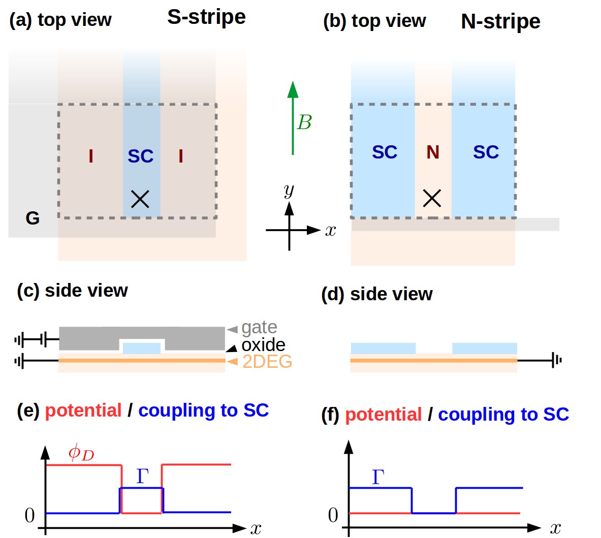
To realize MBSs in such 2DEG structures, one can pursue the two routes sketched in Fig. 1: The first approach is to fabricate a thin stripe of aluminum with a top gate that depletes the normal conducting 2DEG around the stripe, turning it into an insulator [Fig. 1(a)]. In this way, a narrow, quasi-1D superconducting channel is formed under the aluminum (called S-stripe in the following). This corresponds to the device design of the recent experiment Suominen et al. (2017). The other, complementary approach Hell et al. (2017); Pientka et al. (2016) uses a normal conducting channel (called N-stripe in the following) next to two proximitized superconducting regions (SC) [Fig. 1(b)].
Out of these promising developments the question arises which requirements have to be satisfied when designing more complex Majorana devices in 2DEGs. In this paper, we therefore numerically analyze two simple device elements both for N- and S-stripes: two parallel Majorana stripes [Figs. 2(a) and (b)] and a trijunction in a tuning-fork design [Figs. 2(c) and (d)]. The latter design respects the key requirement that all Majorana stripes have to be parallel to stay in the topological regime Hell et al. (2017). We employ a Green’s function approach to compute the local density of states for these devices numerically as explained in Sec. I. This provides relevant information about the excitation spectrum.
Using material parameters taken from experiments, we first investigate in Sec. II single N- and S-type stripes. In both cases, we predict that the channels develop a zero-energy mode when a magnetic field is applied along the stripe. This is a signature of a topological phase transition and formation of a MBS, similar to nanowire setups. Since single N-stripes have recently been investigated theoretically elsewhere Pientka et al. (2016); Hell et al. (2017), we focus our attention mostly to S-stripes. We verify that the effect of realistically smoothened gating potentials hardly affects the energy spectrum, provided the chemical potential can be tuned in the 2DEG. We further show that the potential barrier height affects the topological phase-transition point in S-stripes. This can be exploited to tune the MBS coupling in S-stripes electrically, similar to a recent proposal for N-stripes Hell et al. (2017).
We then show in Sec. III that the MBSs in two parallel stripes can be well separated from each other by applying potential differences of a few meV for stripe distances of 200 nm or more. We further show in Sec. IV how to electrically control MBSs in a trijunction region. A key question is here whether the coupling energies can be tuned sufficiently without introducing unwanted, low-energy excitations. We show, for a specific geometry, that the coupling energies can be tuned between neV and about eV, while excited states remain at tens of eV throughout the entire tuning range.
We finally address in Sec. V the question how to braid MBSs in a 2DEG-based platform both for N- and S-stripes. There are numerous proposals for MBS braiding, which fall into three categories: The first suggestions aimed at moving topological phase boundaries Alicea et al. (2011); Clarke et al. (2011) physically, which, however, produces quasiparticles that prevent quantum-error correction Pedrocchi and DiVincenzo (2015); Pedrocchi et al. (2015). In a second class of approaches, the topological phase boundaries are preserved and braiding is achieved by adiabatic manipulation of the couplings between the MBSs Halperin et al. (2012); Hyart et al. (2013); Aasen et al. (2016); Hell et al. (2016); Sau et al. (2011); van Heck et al. (2012). Finally, the same operation as that of braiding can also be achieved by sequences of measurements of different MBS pairs Bonderson (2013); Vijay and Fu (2016); Karzig et al. (2016). In this paper, we mostly focus on an adiabatic braiding approach closely related to Refs. Aasen et al. (2016) and Sau et al. (2011). From our numerical results for the excitation spectrum, we estimate a time scale for braiding of about 10-100 ns.
I Model and numerical approach
To model the six devices shown in Figs. 1 and 2, we use a Green’s function formalism. In Sec. I.1, we first introduce the 2DEG Green’s function, containing the 2DEG Hamiltonian and the self-energy contribution from the superconducting top layer, which has been integrated out. In contrast to many other studies, we keep finite-frequency corrections to obtain a more accurate description of the energy spectrum. For our numerical calculations, we introduce a lattice and compute the local density of states in the finite regions framed by dashed lines in Figs. 1 and 2. The fainted parts outside this region are assumed to continue infinitely in vertical direction. These are accounted for by a surface Green’s function, which is nonzero on the boundary of the framed regions. Details of our algorithm are relegated to App. A.
I.1 2DEG with proximity-induced superconductivity
The (unproximitized) 2DEG is modeled by a single electron band with effective mass at electro-chemical potential as described by the following Bogoliubov-de Gennes Hamiltonian ():
| (1) | |||||
In the second line, we added the Rashba spin-orbit coupling (with velocity ) and the Zeeman energy () due to a magnetic field. The Hamiltonian acts on the four-component spinor containing the electron and hole components for spin . The Pauli matrices and () act on particle-hole and spin space, respectively.
The proximity effect of the superconducting top layer can by included by integrating out the superconductor in the wide-band limit Sau et al. (2010b); Stanescu et al. (2010); Danon and Flensberg (2015). The resulting retarded Green’s function of the 2DEG is given by
| (2) |
with the retarded superconductor self energy
| (3) |
and prefactor
| (6) |
In our numerical calculations, we replace with a positive smaller than all other energy scales (but we keep the notation in all following expressions).
The self energy is nonzero only where the device is covered by a superconducting layer [blue in Figs. 1 and 2] and for simplicity we assume the tunnel coupling to be uniformly given by a constant in these regions [Fig. 1(e) and (f)]. Note that the Zeeman splitting of the states in the superconducting top layer is neglected because the g factor in the superconductor (2) is smaller than that in the 2DEG (probably 10 Shabani et al. (2016))
Our self energy does not include a proximity-induced shift of the chemical potential under the superconductor. This approximation is motivated by recent experiments Kjaergaard et al. (2016a) revealing that proximity-induced superconductor-normal junctions achieve a high transparency. This indicates that the mismatch in the chemical potential must be rather small.
Unless stated otherwise, we keep the frequency () dependence of the self energy, which leads to a downward renormalization of all non-zero energies Deng et al. (2016); van Heck et al. (2016). This affects our estimates of coupling energies and energy gaps and translates directly into the time scales needed for adiabatic manipulation. Moreover, the self energy becomes imaginary for energies , i. e., when the states in the 2DEG can also leak into the superconducting top layer.
I.2 Tight-binding model and Green’s function formalism
We simulate the devices numerically by introducing a 2D lattice and applying a recursive Green’s function formalism Ferry and Goodnick (1997) to compute the density of states in the regions of interest. Since our approach follows that of Ref. Wimmer, 2008, we just sketch its central idea here and refer the reader to Ref. Wimmer, 2008 for further details.
First, the discretized versions of the Hamiltonian and the superconductor self energy take the form:
| (7) | |||||
| (8) |
Here, the subscript denotes the sites in the central region of interest [surrounded by dashed lines in Figs. 1 and 2], which has () sites in the - (-) direction. The subscript denotes all other sites outside. We give concrete expressions for the discretized versions of and in App. A.1. Notably, the self energy is local in space and thus does not contribute to the coupling of the central and outer region.
To extract MBS coupling energies and topological energy gaps, we compute the local density of states in the central region as a function of energy . The local density of states is obtained from the retarded Green’s function:
| (9) |
Here, the trace runs over particle-hole and spin indices and and refer to the lattice point. The normalization constant has been chosen such that . We note that the local density of states below the superconducting gap can be probed directly by tunneling spectroscopy in the limit that the tunnel coupling between probe and 2DEG is much smaller than temperature. All peaks are then broadened by temperature. To obtain a measure for the excitation spectrum of the central region, we also investigate the total density of states given by
| (10) |
where due to the normalization .
The Green’s function can be found from a Dyson equation derived with as a perturbation Wimmer (2008):
| (11) |
Here, is the self energy describing the effect of the outer region on the central region. It is nonzero only on the boundary lattice sites of the central region. Based on Ref. Wimmer, 2008, we explain in App. A.2 how can be obtained from solving a rather simple eigenvalue problem. Once has been determined, one can in principle compute through the inverse in Eq. (A.3) to find the local density of states in the central region. However, since one actually needs only the the lattice-diagonal entries of to compute , one can apply a more efficient recursive technique to determine these entries. This is further discussed in App. A.3.
II Single Majorana stripe
To start our analysis of the Majorana devices, we first briefly compare the topological phase transition and energy spectrum in semi-infinite S- and N-stripes. We show that a MBS located at the end of a semi-infinite stripe appears when increasing the magnetic field along the stripe. We further show that the phase-transition point can be tuned with the confinement potential, which can be used to couple the MBSs in N- or S-stripes electrically.
II.1 S-Majorana stripes
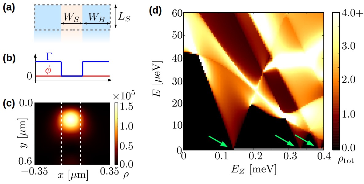
We first consider an S-type Majorana stripe [Fig. 3(a)]. We assume a top gate that covers the stripe and the region in their vicinity. The top gate creates a potential well [Fig. 3(b)], which is incorporated in our numerical calculations by lowering the chemical potential in the unproximitized region [brown in Fig. 3(b)], while the chemical potential under the superconductor [blue in Fig. 3(b)] is assumed to be unaffected. Such a steep potential drop is motivated by the good screening effects of the superconductor. In App. C, we verify that a realistically smoothened gate-induced potential profile has only a minor influence on the resulting energy spectrum. The potential we use there is a solution of Poisson’s equation assuming zero charge density in the 2DEG. This approximation is valid in the low charge-density regime considered in this paper.
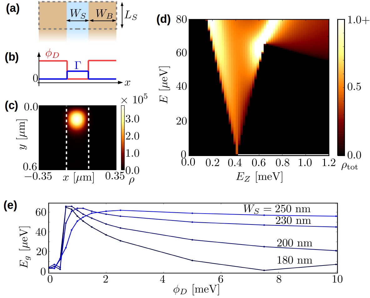
We next investigate the topological phase transition in an S-stripe by inspecting the total density of states as a function of energy and Zeeman energy [Fig. 3(d)]. The gap to the energy continuum of states closes and re-opens at a critical Zeeman energy of . This value is confirmed by an analytic estimate derived in App. B:
| (12) |
Here, characterizes the transverse extent of the wave function. This extent can be estimated by , where is the decay length into the depleted region. Using the parameters of Fig. 3, and estimating the decay length by (i.e., neglecting magnetic field and spin-orbit coupling in the estimate), we obtain in good agreement with the numerical result. Note that Eq. (12) actually tends to overestimate because it assumes that the proximity-induced superconductivity with strength acts on the entire extent of the wave function.
When the Zeeman energies exceeds the critical value, , the density of states exhibits a peak at zero energy [Fig. 3(d)]. The corresponding local density of states at zero energy is localized at the end of the stripe [Fig. 3(c)]. This peak is due to a MBS that appears at the end of the semi-infinite stripe 111Our findings do not strictly prove a topological phase transition at but this interpretation is in line with other works modeling nanowires (see, for example, Lutchyn et al. (2011)). . We can further see that the topological energy gap – the energy of the lowest excited state – remains stable for and reaches a value of about . This illustrates that a sizable fraction of the tunnel coupling and the superconducting gap of the parent superconductor can be reached in an S-type geometry.
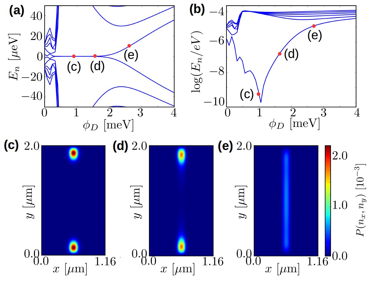
Interestingly, the topological energy gap reaches a maximum as a function of the potential barrier [Fig. 3(e)]. This feature is related to the tunability of the phase transition point as explained below in this paragraph. Depending on the stripe width, the topological energy gap may be suppressed or it may remain nearly constant for increasing potential barrier heights . The reason for this is that changes the decay length of the wave function in the barrier region and thus its transverse extent . From Eq. (12), it is clear that this can tune the system through a phase transition for fixed magnetic field . Solving Eq. (12) for using the same parameters as before, we find a critical extent of . To estimate the gate-tunability of , we first note that when raising the barriers to large values and is increased by lowering the barriers. Using a value of , which is roughly what is needed to form bound states in the stripe [Fig. 3(d)], we obtain . This means that can be roughly tuned in a range of 120 nm using the depletion gates.
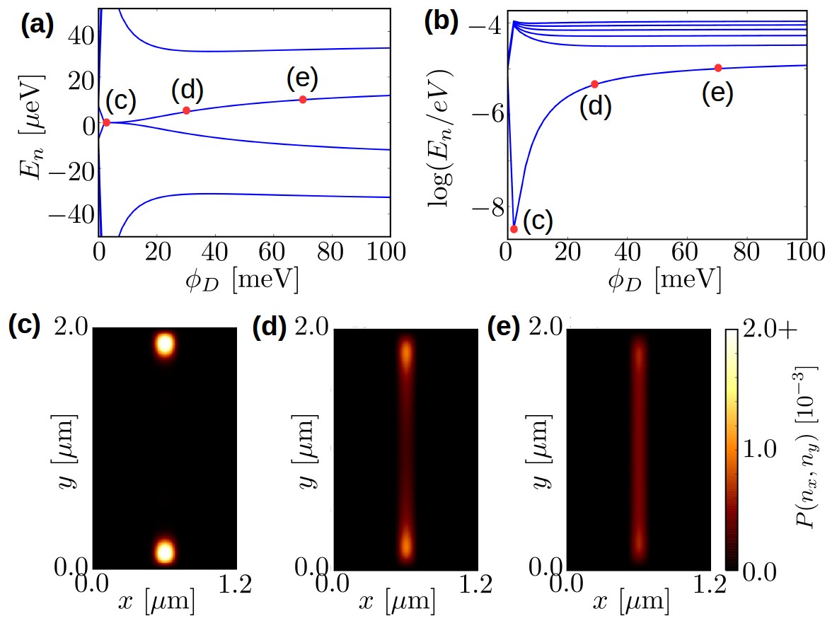
Our estimates are confirmed by further numerical calculations [Fig. 4]. For this purpose, we numerically diagonalized the Hamiltonian (1) in a finite region with the added zero-frequency self energy . For simplicity, we neglect finite-frequency corrections here. For a stripe width , the MBSs split in energy when increasing the barrier to about 10 meV [Fig. 4 (a)]. We see that the related probability density can be tuned from localized MBSs [Fig. 4(c)] over overlapping MBSs wave functions [Fig. 4(d)] to an Andreev bound state that is extended along the S-stripe [Fig. 4(e)]. This means that the MBSs can be controlled electrically: The corresponding energy of the state can be tuned in a large range between about 1 neV to a more than 10 eV for large barriers [Fig. 4(b)]. Using a smaller stripe width, one can couple the MBSs for smaller values of [see App. B]. However, for separating adjacent S-stripes from each other, it may be advantageous if the MBS coupling is suppressed over a larger range of . We therefore use in the following calculations and for S-stripe devices.
II.2 N-Majorana stripes
We next compare the spectral properties of S-stripes with those of N-stripes [Fig. 5(a)]. Since single N-stripes have been thoroughly discussed before Hell et al. (2017); Pientka et al. (2016), we keep our discussion here brief. For a discussion of the gate control of the MBS coupling in N-stripes see Ref. Hell et al., 2017.
Similar to S-stripes, we also find a closing and a re-opening of the energy gap at about eV [Fig. 5(d), left green arrow]. Again, a zero-energy peak appears in the total density of states with a local density [Fig. 5(c)] similar to that for S stripes. This MBS peak even persists when the gap closes and re-opens a second and a third time at eV and eV, respectively [Fig. 5(d), middle and right green arrow]. This is probably due to to co-existence of two or three MBSs per end, which is a consequence of the additional spatial mirror symmetry of the device, which is therefore in symmetry class BDI Hell et al. (2017); Pientka et al. (2016).
However, there are also differences in the characteristics of S- and N-stripes. First, the critical Zeeman field in N-stripes, eV, is below 2 and thus smaller than that for S-stripes, which is expected to be larger than 2. As explained in Ref. Hell et al. (2017), the lower value of is due to the weakened superconducting proximity effect in the normal region. This is an advantage for reaching the topological regime as one strives to minimize the required magnetic fields. However, the magnetic field range that results in a sizable energy gap to excited states is smaller than that in S-stripes. Furthermore, the energy gap to the excited states is smaller (about 20 eV at eV) than that for S-stripes. However, it can be increased by asymmetric N-stripe designs as shown numerically Hell et al. (2017) (see also Fig. 7). This shows that engineering MBSs in N-stripes should also be possible but requires more optimization than in S-stripes.
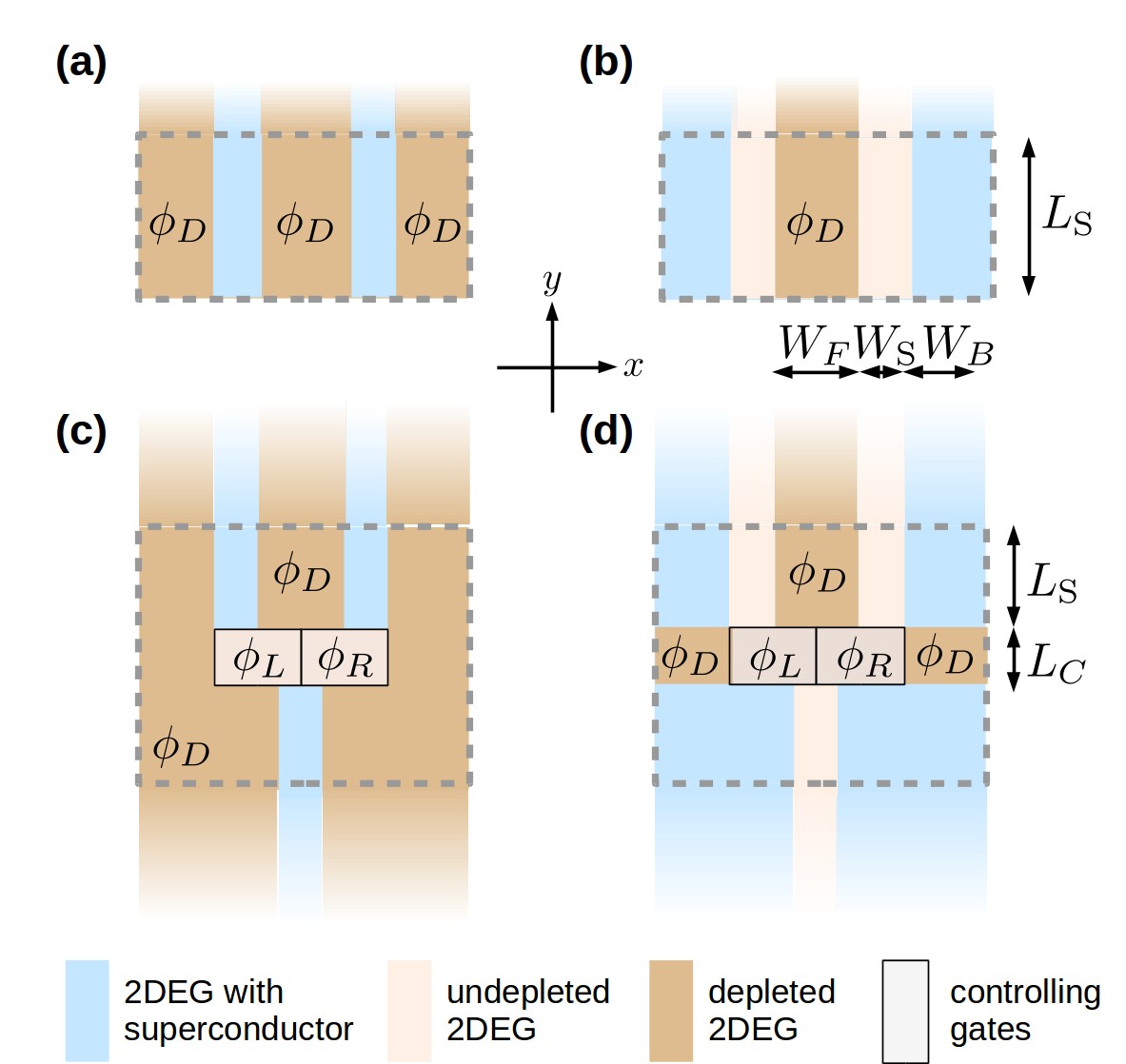
III Parallel Majorana stripes
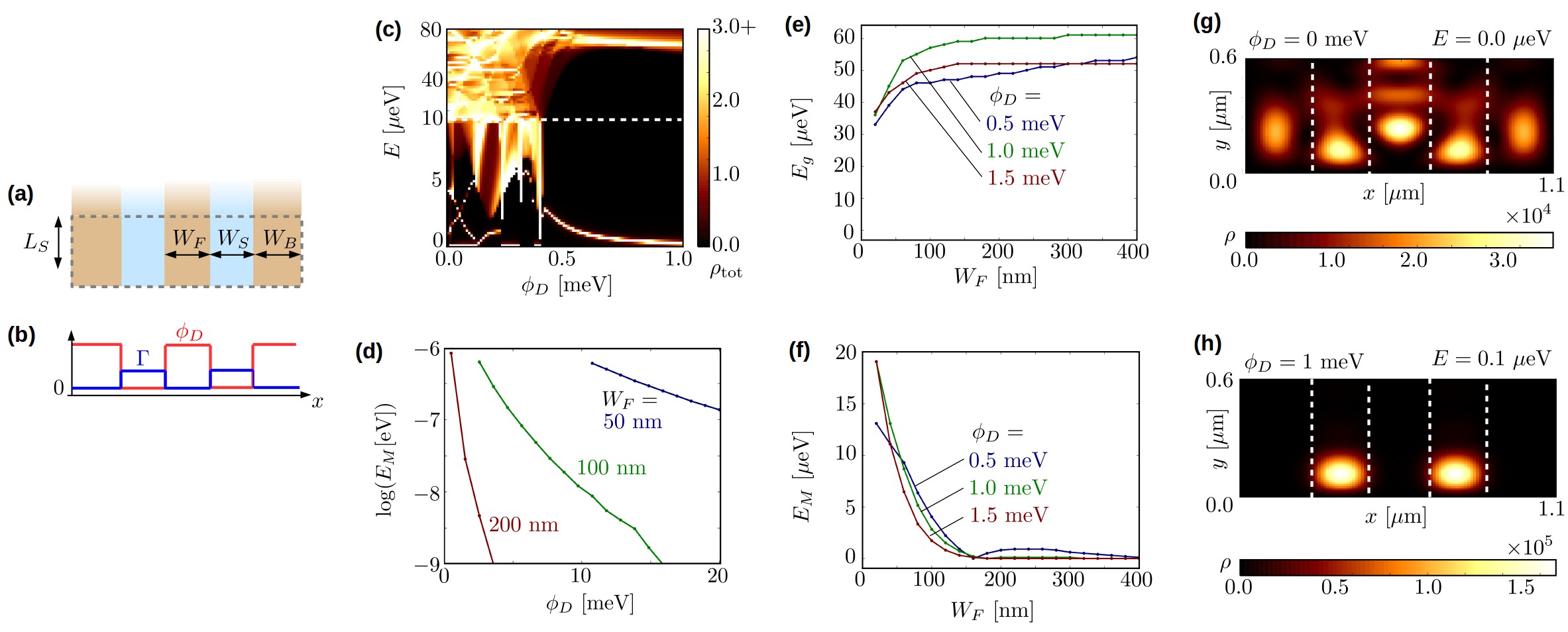
To build more complex Majorana devices or even Majorana networks, it is important to specify how close two Majorana stripes can be placed next to each other. The coupling energy of the MBSs from the two stripes should be suppressed as much as possible, while the energy gap to excited states should remain as large as possible. Considering next two Majorana stripes in parallel [Figs. 2(a) and (b)], we show that the MBSs are well separated for stripe distances of about 200 nm and moderate potential differences on the scale of a few meV. This geometrical constraint is also relevant for the design of a trijunction in a tuning-fork geometry discussed in Sec. IV.
III.1 S-Majorana stripes
We first discuss two parallel S-stripes [Fig. 6(a)], where a single top gate covers both stripes. As before, we assume that the gate voltage shifts the chemical potential only where the 2DEG is not covered with a superconductor [Fig. 6(b)].
The potential-barrier dependence of the total density of states is depicted in Fig. 6(c). For the parameters used in this case, the density of states changes drastically around . Below this value, the density of states is nonzero nearly in the entire energy range and the local density of states is not localized in the stripe regions [Fig. 6(g)]. The lower edge of the continuum of states is suppressed to less than eV and we find a few discrete states below that. The small remaining energy gap to the continuum is probably due to the finite width of the device in direction perpendicular to the stripes. This leads to a small confinement energy of .
By contrast, for potential barriers above the threshold , the regions without top superconductor are depleted. While this threshold certainly depends on the parameters of the system, it corresponds to an energy comparable to the induced superconducting gap and the spin-orbit energy and we therefore expect it to hold more generally. The density of states has a peak approaching zero energy that persists for all in the range shown. This peak can be attributed to two slightly overlapping MBS whose local density of states is confined to the stripe region [Fig. 6(h)].
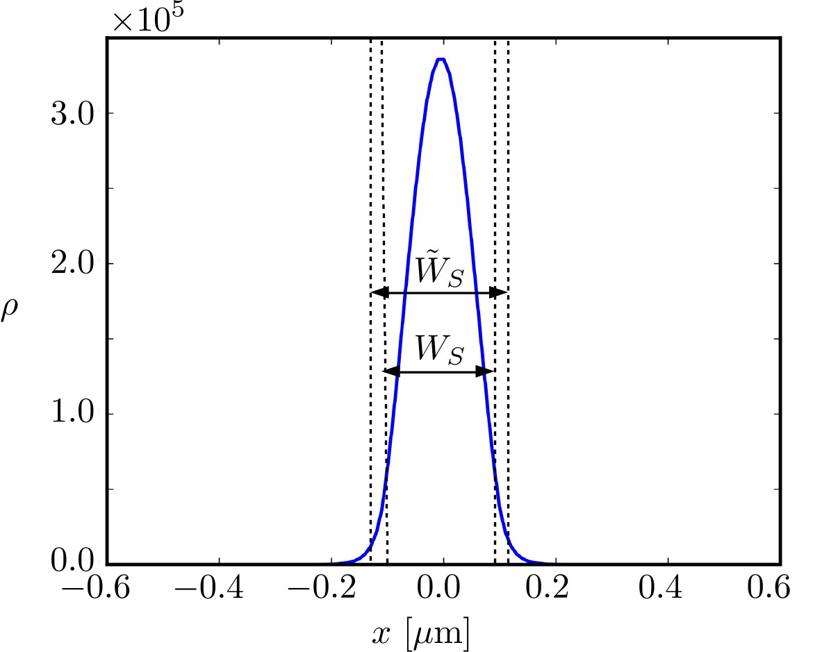
The coupling between the MBSs can be efficiently suppressed by increasing the potential barrier or the separation of the stripes. We determine the coupling energy of neighboring MBS as the position of the first peak in the total density of states [extraction procedure explained in Fig. 6]. Specifically, we find that for a stripe separation of , a potential barrier of only a few meV is needed to suppress the Majorana coupling to the neV range [Fig. 6(d)]. We further find that stays below about 1 eV for stripe separations of about for potential barriers as low as [Fig. 6(f)]. However, to reach the neV range for separations much smaller than 100 nm requires much larger potential barriers [Fig. 6(d)].
We next investigate the behavior of the energy of the lowest excited states. We can see that for potential barriers , the threshold of the continuum is pushed up to about eV [Fig. 6(c)]. Furthermore, increases with the separation and clearly depends on the height of the potential barrier [Fig. 6(e)], similar to what has been found for the single S-stripes [Fig. 3(e)]. We checked that even for larger values , as used in Fig. 6(d), the topological gap remains large (The intra-stripe coupling of the MBS is ignored here, compare Fig. 4).
III.2 N-Majorana stripes
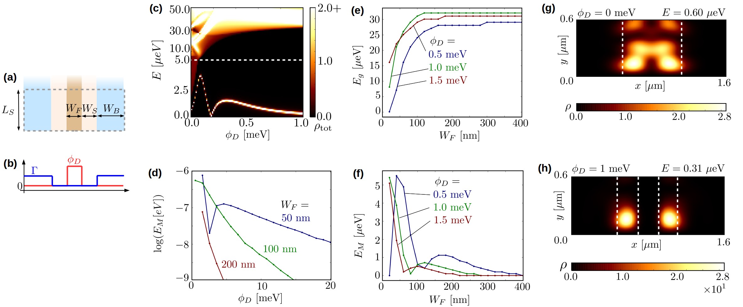
We next discuss a configuration of two N-stripes in parallel [Fig. 7(a)]. Here, we consider a gate which depletes a non-superconducting region between the two stripes [Fig. 7(b)]. We show next that the N stripes can be separated with similar parameter choices as for the S stripes.
First, at zero potential difference, , the 2DEG region without top superconductor forms one wider stripe and the total density of states is nearly gapless. However, the density of states is small at low energies [dark red in the color scale of Fig. 7(c) for small ]. The corresponding local density of states spreads over the entire 2DEG region without top superconductor [Fig. 7(g)].
For nonzero potential barrier, the lower edge of the continuum of excited states raises quickly to higher energies. The total density of states features furthermore a discrete peak at energy , which approaches zero energy [Fig. 7(c)]. The local density of states at this peak is clearly localized at the ends of both stripes [Fig. 7(h)], i.e., the wider stripe is cut into two when increasing . We interpret the energy again as the coupling energy of the MBSs localized at the ends of the two stripes. Similar to S-stripes, this coupling energy can be strongly suppressed by increasing [Fig. 7(d)]. Again, reaches the sub-neV range for stripe separations of 200 nm and of a few meV. We further find that the Majorana coupling energy is suppressed when increasing the stripe distance [Fig. 7(f)]. By comparing these results to that for S-stripes, it seems that similar potential barriers and stripe distances are needed to ensure a good separation in the case of N-stripes.
We finally investigate the parameter dependence of the lower edge of the excited-state continuum. The energy reaches a value around 20 eV for potential differences around 1 meV [Fig. 7(e)], so that the barrier exceeds all other energy scales. This value is somewhat larger than what we found for for the single-stripe case [Fig. 5]. This is consistent with Ref. Hell et al. (2017), which showed that an asymmetric design of a single N stripe with a proximity-induced superconductor on one side and a gate on the other leads to a larger topological gap than a device with superconducting regions on both sides. Yet, the energy gap for N-stripes is smaller than that for S-stripes, which is expected due to the weaker superconducting proximity effect for N stripes (see Sec. II.2).
IV Trijunctions: Tuning-fork design
We next discuss the design of a trijunction using Majorana stripes [Figs. 2(c) and (d)]. An important design constraint discussed in Ref. Hell et al., 2017 is that all Majorana stripes have to placed in parallel 222This has been discussed for N-stripes in the supplemental material of Ref. Hell et al., 2017. . The reason is that the topological energy gap closes when the magnetic field direction deviates from the long stripe direction by more than about 10 degrees. This is why we investigate a tuning-fork shaped structure as sketched in Figs. 2(c) and (d). This raises the crucial question whether topologically trivial low-lying excited states occur in the central coupling region, which would be detrimental to the operation of this Majorana device. We show here for specific examples for both S- and N-type designs that this can be avoided while controlling the MBS coupling energies between neV and eV using electric gates. The energy gap to the excited states remains throughout larger than 10 eV.
IV.1 S-Majorana stripes
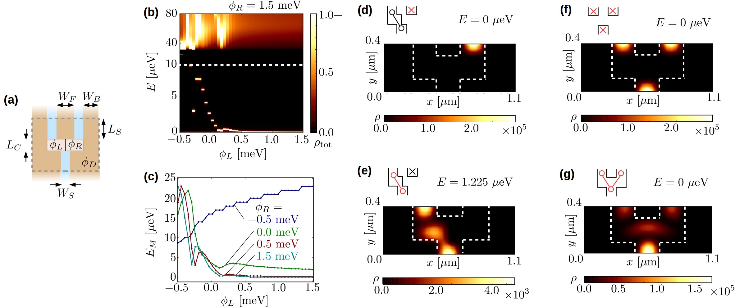
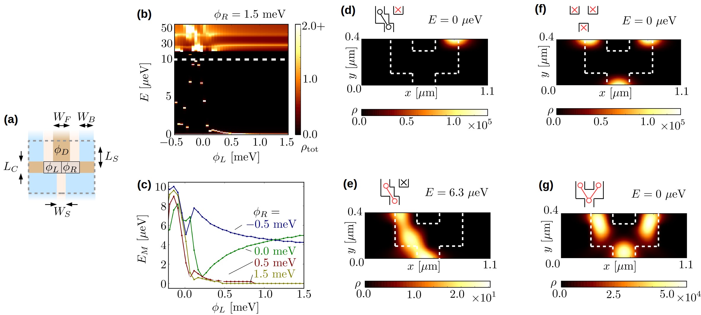
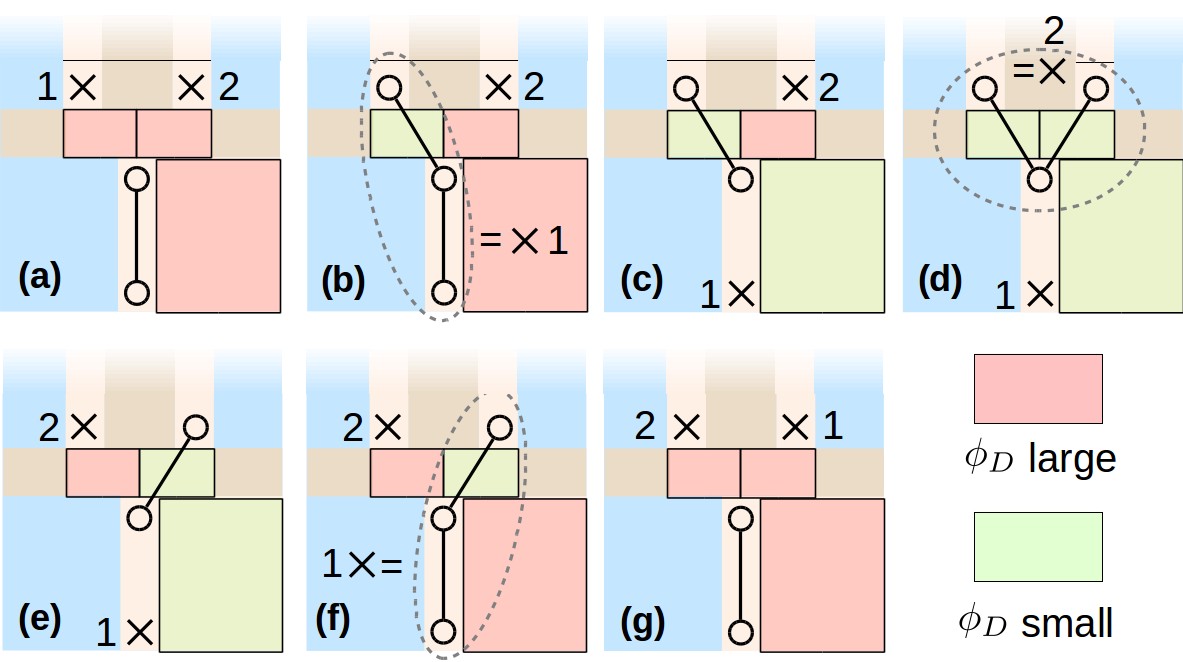
We first investigate an S-stripe trijunction [Fig. 8(a)]: The 2DEG regions without a superconducting top layer are depleted by a top gate except for a central region connecting the three stripes. In this region, two additional gate ’fingers’ with different voltages are integrated, which are isolated from each other. They affect only the central part by coupling the left and right upper stripe to the lower stripe. Such gates could be fabricated, for example, by adding a second metallization layer on top the superconducting film and the depletion gate. For the concrete devices studied in this section, these two gate ’fingers’ would have a width of 200 nm, which should be achievable with present-day fabrication technologies.
To discuss the voltage control of the MBS coupling, we start from the situation when the channel connecting the right and lower stripe is depleted (), while the gate controlling the channel connecting the left and the lower stripe is changed. When is around zero or below, we can discern two discrete peaks below the threshold to the continuum of states [Fig. 8(b)]. One of the peaks is at zero energy [hardly visible in Fig. 8(b)] and the corresponding local density of states is localized at the end of the right stripe [Fig. 8(d)]. We interpret this feature as a MBS at the end of the right stripe, which cannot couple to the other MBS in this gating configuration. The second peak is at a few eV and the corresponding local density of states is delocalized between the lower and the left stripe [Fig. 8(e)]. We attribute this peak to a coupling of the two MBSs at the end of the lower and left stripe. They form a fermionic mode at energy . When lowering to meV, the coupling energy increases up to about 20 [Fig. 8(c)].
The energy of the mode formed by the two coupled MBSs can be controlled by the left gate [Fig. 8(b) and (c)]. When increasing the potential height , the energy of this mode approaches zero. For , the two MBSs are separated and the local density of states at zero energy shows three peaks at each end of the three stripes [Fig. 8(f)]. The peak energy reaches a value below 1 neV at meV (not shown).
Moreover, the lower edge of the continuum of excited states stays rather constant at about when increasing [Fig. 8(b)]. This means that one can can tune the coupling between the left and lower MBSs without introducing low-lying excitations and keep the right MBS separated. The value for is somewhat reduced as compared to Figs. 3 and 6 because we use a larger depletion potential here, which moves the system closer to the phase-transition point. This larger value of reduces the MBS coupling between the parallel Majorana stripes. This is needed to reach coupling energies on the neV range as discussed in Sec. III.1.
Finally, by lowering the potential on the right part, the right MBS can couple to the other ones. At , the three MBSs form one MBS with a zero-energy peak in the density of states. The corresponding local density of states is delocalized over all three stripes [Fig. 8(g)]. In addition, the MBSs form a fermionic mode leading to a peak in the density of states at a finite energy . The energy of this mode can be increased above 10 eV by lowering to negative values [Fig. 8(c)]. As is increased and the left MBS is decoupled, even increases. We checked that the lowest value of further excited states stays rather constant at about 30 also for reduced , similar to Fig. 8(b). This implies that one can also tune between three and two coupled MBSs without introducing low-lying excited states.
IV.2 N-Majorana stripes
We finally discuss a trijunction formed by three N-stripes [Fig. 9(a)]. We show that one can gain voltage control over the MBSs in an N-stripe trijunction very similar to the S-stripe trijunction and compare the device operation and coupling energies for both designs.
We consider again a tuning-fork shaped device similar to that for S-stripes [Sec. IV.1]. The geometrical dimensions of both devices considered differ only in that the separation of the two upper stripes is slightly larger for the N-stripes. The finger gates again only control the central part. However, one has to deplete the regions left and right to the central part in addition to the region between the two upper N-stripes. Alternatively, one could disconnect the different parts by etching the 2DEG. Separating the three Majorana stripes in this way is crucial for the proper operation of the device: Just replacing these parts by a superconducting top layer is not sufficient as discussed below in this section.
We start our discussion of the gate control again for the situation when the right stripe is decoupled from the lower and the left one by choosing meV. The corresponding total density of states has a zero-energy peak for all values of [Fig. 9(b)]. In analogy to the S-stripe trijunction, we find that the local density of states is localized in the right stripe for [Fig. 9(d)], which corresponds again to a decoupled MBS in the right stripe 333In contrast to the S-stripes, we can see that the local density of states is not centered in the middle of the upper N-stripes The reason is the asymmetric device design in this case: The MBSs can extend somewhat into the region with proximitized-induced superconductivity, while they cannot penetrate the depleted region in the middle between the upper stripes.. The two MBSs in the lower and left stripe are coupled and lead to a peak in the density of states at finite energy [Fig. 9(b)]. At the peak energy , the local density of states is indeed distributed over both stripes and the central region [Fig. 9(e)]. By increasing , the discrete peak in the total density of states approaches zero energy [Fig. 9(b)]. It reaches a value of about 0.5 at meV (not shown). The local density of states at zero energy shows three disconnected peaks in this case, corresponding to three isolated MBSs [Fig. 9(f)].
If we next lower to , we can see that the peak energy does not drop to zero as is increased [Fig. 9(c)] but stays at about eV, somewhat smaller than for S-stripes. In addition, a zero-energy peak remains in the total density of states throughout, which is not shown here. This peak corresponds to a MBS formed from a superposition of the three MBSs in the three stripes as the local density of states illustrates [Fig. 9(g)].
We note that the gate control works properly only if the two regions left and right of the central coupling region are depleted. If the depletion gates there are replaced by a superconducting top layer (but keeping device the same otherwise), we find a peak energy of about eV (not shown here). This peak energy cannot be suppressed further by increasing the potential barriers or . This is consequence of an undesired coupling of the MBSs in the upper and lower stripe through the region with proximity-induced superconductivity. The barrier induced by the superconductor (here about 0.2 meV) is not enough to separate the stripes sufficiently.
One could also imagine that the potential in the depleted regions left and right of the center region was also controlled with the gates. This would have the advantage that only a single gate was needed on each side of the trijunction. However, one loses good control over the MBS coupling energies in this case. We checked from numerical calculations (not shown) that in this case the energy gap to the excited states is suppressed for low and when the MBS coupling becomes sizable. One may explain this feature by considering that the confinement energy in the direction perpendicular to the wires is decreased in this case. One then essentially creates a channel for electrons perpendicular to the magnetic field. From our results in Ref. Hell et al. (2017), we know that the topological energy gap closes when the magnetic field is perpendicular to the stripe.
Finally, our numerical calculation shows that there remains a gap to the continuum of excited states [Fig. 9(b)], also when is reduced (not shown). However, we can see that this energy gap is smaller than that for the S-stripe design: For all potentials , the continuum of excited states appears at eV, a value that is comparable to the value in Fig. 5 and most probably limited by the symmetric design of the lower Majorana stripe. We expect that could be increased somewhat by an asymmetric device geometry for the lower stripe (see Sec. III.2).
V Time scales for braiding
Based on our numerical results from above, we finally discuss the time scales for braiding MBSs in the two trijunction designs. The protocol we consider is sketched in Fig. 10 and relies on adiabatic manipulation of the coupling energies of the MBSs Aasen et al. (2016); Sau et al. (2011). In addition to the control of the MBS coupling in the central region of the trijunction, braiding also requires control over the MBS coupling within a Majorana stripe, both for initialization and readout as well as the braiding steps themselves. Before turning to the time scales in Sec. V.2, we first discuss the intra-stripe coupling strategies in Sec. V.1.
V.1 Gate-voltage control over intra-stripe Majorana bound state couplings
The MBS coupling within the Majorana stripes can be tuned in two ways, namely by (i) tuning the Majorana wave function overlap, or by (ii) tuning the Coulomb interaction in the wire.
The first strategy can be achieved by a gate-controlled tuning of the effective stripe width as discussed for S-stripes in Sec. II.1 and for N-stripes in Ref. Hell et al., 2017. In both cases, one can tune the MBS coupling energies between about 1 neV or less to about eV or larger, while maintaining a gap to the excited states larger than eV. This is comparable to the results for the trijunction region.
The second strategy to gain control over the MBS coupling would be to take advantage of Coulomb blockade physics, similar to proposals based on nanowires Aasen et al. (2016); Hell et al. (2016). The idea is to electrically isolate the Majorana stripe from its surrounding, turning it into an island with a capacitance . The related charging energy sets the scale for the maximally achievable MBS coupling energies. To estimate , we assume that the capacitive coupling of the superconducting layer to the top depletion gate gives the dominant contribution to the total capacitance . We thus obtain for a parallel-plate capacitor, where is the vacuum permittivity and is the permittivity. Furthermore, is the thickness of the aluminum oxide layer separating the superconductor and the top gate, is the width, and the length of the Majorana stripe. Using , , , and [as in Fig. 4], we obtain .
To reduce the MBS coupling energy, one would couple the superconducting top layer to a bulk superconductor by a gated semiconductor junction. Based on Eq. (5) in Ref. Aasen et al., 2016, one could expect a coupling energy of neV for meV, while the gap to the excited states is always larger than . With this estimate, we see that charging effects may provide an alternative to control the coupling of MBSs not only in nanowire setups, but also in 2DEG structures.
V.2 Time scales constraints from trijunction tuning
We finally turn to the discussion of the times scales for braiding. A rough estimate of the time scale needed to carry out the steps of the braiding protocol is given by
| (13) |
Here, is the energy of the MBSs close to zero energy, is the energy of the fermionic mode formed from coupled MBSs (as sketched in Fig. 10, at least two MBSs always remain coupled), and is the energy gap to other excited states.
As we have shown above for both N- and S-stripe designs, the minimal MBS coupling energies in the trijunction region can be suppressed to , which translates into an upper time scale of about
| (14) |
Our findings also indicate that coupling energies of are possible, which are always lower than . This yields a lower time scale of
This means, as mentioned initially, that the steps of the braiding protocol can be carried out on a time scale of about 10-100 ns. The coupling energies of about 10 eV correspond to a temperature of about 120 mK. To initialize the system, one has to cool below this temperature, which is experimentally demanding but possible. The time-scale window derived here might be even wider by optimizing the tuning-fork control further, especially with somewhat increased coupling energies.
V.3 Conclusion
In this work, we have shown that the coupling of Majorana bound states (MBSs) in simple network components formed in two-dimensional electron gases (2DEGs) can be controlled electrically. MBSs can be created at the ends of topological quasi-1D channels in two different designs, namely (i) in S-stripes (top Al stripe above the channel) and (ii) N-stripes (top Al next to the channel).
We showed that the coupling between parallel Majorana stripes can be suppressed for separations of a few hundred nanometers using potential barriers on the meV scale. MBSs can further be coupled in trijunction in a tuning-fork shape. We showed that gate control can be used to tune the coupling of MBSs within a Majorana stripe and between different stripes in a range from 1 neV to about 10 eV. At the same time, a sizable topological energy gap can be retained (tens of eV), which depends on the potential confining the topological channels.
To realize a trijunction in a 2DEG-based platform, it is important to use a tuning-fork as depicted in Fig. 2(c) and (d) because the topological gap is very sensitive to a misalignment of the stripe and magnetic field direction. It is also important to separate the different stripes from each other through potential barriers of a few meV, i.e., barriers larger than typical induced superconducting gaps. This is needed to avoid uncontrolled couplings between the MBS. The precise dimensions of the tuning fork may, by contrast, vary somewhat and are not tied to the specific example discussed in this paper. However, using sharp potential barriers, the stripe width has to be between 150 - 200 nm to achieve a control over the MBS coupling within a stripe (at zero chemical potential and experimentally motivated parameters used here).
Based on our numerical calculations, we estimate that an adiabatic braiding protocol can be carried out in a time window of 10-100 ns. Moreover, the findings of our study are useful for Majorana box qubits Plugge et al. (2017) and related network designs Vijay and Fu (2016); Karzig et al. (2016) aiming at readout-based braiding. These proposals involve quantum dots, which could be easily integrated into a 2DEG-based platform. 2DEGs may thus provide an alternative route to build more complex Majorana devices with the additional advantage of flexibility in fabrication as compared to other platforms.
Acknowledgements.
We acknowledge stimulating discussions with M. Kjaergaard, P. Kotetes, C. M. Marcus, F. Nichele, A. Stern, and H. J. Suominen, and support from the Crafoord Foundation (M. L. and M. H.), the Swedish Research Council (M. L.), and The Danish National Research Foundation.Appendix A Green’s function approach
A.1 Two-dimensional tight-binding model
Our tight-binding model is obtained by discretizing the continuous spatial coordinates as a lattice with points , where denotes the lattice constant. Due to the discretization, we have to replace the derivatives by finite differences Ferry and Goodnick (1997):
| (15) | |||||
| (16) |
Analogous formulas apply for the derivative. Using this procedure, we can rewrite the Hamiltonian (1) and the retarded self energy (3) in tight-binding approximation. Defining the hopping amplitudes
| (17) |
they read
| (18) | |||||
| (19) |
Here, denotes a state with an electron () or hole () with spin localized at lattice point . We introduce the short-hand notations , , , and the factor Sau et al. (2010b)
| (20) |
with the prefactor
| (23) |
In the limit , we obtain and the pairing term in Eq. (19) is . However, in nearly all our calculations we keep finite-frequency corrections, which leads to modifications of the pairing term at finite energy.
A.2 Self energy of semi-infinite outer regions
In our numerical approach, we divide the system into a central part of interest (lattice points with and ) and an outer region that is integrated out. In this Appendix, we explain how to compute the retarded self energy of the outer regions, entering into Eq. (A.3), by solving a rather simple eigenvalue problem Wimmer (2008).
Based on Eqs. (7) and (8), one can derive a Dyson equation with as perturbation and one can show that the retarded self energy can be expressed as:
| (24) |
This expression contains the Green’s function of the outer region in the absence of a coupling to the central region:
| (25) |
Since couples only nearest-neighbor sites, one actually only needs the Green’s function evaluated at the sites adjacent to the central region, . We assumed her for simplicity that the outer region covers the lattice sites as, for example, in Fig. 1.
To derive an expression for , we can follow the steps given in Ref. Wimmer, 2008 while additionally accounting for the by defining a ’Hamiltonian’ . The basic idea to compute is to express it terms of the eigenbasis of . For this, one uses that has a tridiagonal form in the lattice points along the direction:
Here, and are matrices. For simplicity, we consider here the semi-infinite region for the parallel stripes in Figs. 2(a) and (b); for the tuning-fork setups has to extend also for . Note that only modifies the diagonal block in Eq. (A.2). It can then be shown that the surface Green’s function satisfies the relation
| (27) |
provided can be inverted, which is possible in our case. The matrices and are obtained from the solutions of the following eigenvalue problem:
| (34) |
The eigenvalues in this equation, , are connected to the ’wave vectors’ of the eigensolutions of when extended infinitely in both directions [by omitting the restriction in Eq. (A.2)]. Of all eigensolutions, one selects those that decay () or propagate (, ) in the positive direction, which we denote by a subscript ’’. The corresponding eigenvalues fill the diagonal entries of and the eigenvectors are contained in . There exist exactly solutions of type ’’ because for every solution of Eq. (LABEL:eq:genev), also is a solution (not shown here). Once has been determined from Eq. (27), it can be inserted into Eq. (24) and the desired self energy can be computed.
A.3 Recursive Green’s function method
In principle, one can compute the Green’s function of the central region by computing the inverse in its definition:
| (36) |
However, computing this inverse is computationally demanding and, in fact, one does not need the diagonal entries to compute the local density of states, Eq. (9). We suppress here the energy argument of the Green’s function to simplify the expressions. In this Appendix, we show how to compute recursively, where has to be understood as taking partial matrix elements.
To start with, we consider the system as a quasi-1D chain in direction with each lattice point associated with a -dimensional subspace. The idea is to exploit the fact that the inverse Green’s function has block-tridiagonal structure along the chain in -direction:
We next define
| (38) |
which satisfies by definition the following equation:
| (39) |
Our goal is to compute . For this, we insert Eq. (A.3) into Eq. (39) and project on . This yields for
| (40) | |||||
with the definitions . One can solve this system of linear equations by Gaussian elimination. Let us simplicity assume . Starting from Eq. (40) for , we can first solve for , insert the resulting expression into Eq. (40) for , solve for , and so on. Repeating this procedure, one can show the following recursion relation by induction:
| (41) | |||||
| (42) | |||||
| (43) |
Proceeding analogously when starting from Eq. (40) for , one obtains a second recursion relation:
| (44) | |||||
| (45) | |||||
| (46) |
Finally, using Eq. (40) for , we obtain
Note that all the above equations also hold for . Thus, we have to iterate Eqs. (42) and (45) starting from Eqs. (43) and (46) until we obtain and , respectively, and insert these into Eq. (A.3) to obtain the the component we are interested in.
This is an efficient approach to compute the diagonal matrix elements of the Green’s function: While Eq. (36) requires the inversion of a matrix, the recursive method requires inversions of matrices. Note that the iterations given by Eqs. (42) and (45) do not have to be repeated all the way to obtain for different . For example, if and are known from calculating , then one only needs to compute from applying Eq. (42) once. The component is obtained using and , where is already known from computing .
Appendix B Topological phase-transition point for S-stripes
We derive in App. B.1 an approximate formula for the condition for a topological phase transition in S-stripes. Based in this, we show in App. B.2 that a gate-controlled phase transition can be evoked for rather small changes in the confinement potential. This complements the example discussed in the main part [Fig. 4], where we focused on an example where rather large gating potentials are needed.
B.1 Condition for phase transition
We start from the full Hamiltonian (1) extended to infinity in all directions. In this case, we can replace , since the momentum in the stripe direction is conserved. A topological phase transition point requires a closing of the superconducting gap at Hell et al. (2017). Using the notation of Sec. I, the Hamiltonian reads for :
| (48) | |||||
where the effect of the gating is absorbed a position-dependent electro-chemical potential with electrostatic potential . The second line incorporates the superconducting proximity effect through an additional pairing term, which is the zero-energy limit of the self energy, i.e., . This replacement introduces no additional approximation as we are only interested in the position of zero-energy eigenstates.
To find the eigenenergies of Eq. (48), we next apply a unitary transformation , which turns the spin-orbit coupling term into a shift of the electrochemical potential Pientka et al. (2016):
To obtain a simple estimate of the eigenenergies, we assume that the wave function is confined by a hard wall in a range . We allow this effective width to larger than the width of the superconducting stripe to account for a nonzero decay length into the barrier region. A simple estimate is . To simplify the procedure further, we assume that the superconducting pairing is uniform, . This allows us to find the eigenstates of Eq. (B.1) from the ansatz with a spinor . Solutions satisfy , with eigenenergies
| (50) |
The lowest bound state for crosses zero energy under the condition
| (51) |
This formula holds strictly only under the condition and has been used in the discussion in Sec. II.1. We note that the actual superconducting proximity effect should also be weaker than what we used in the above estimate because the wave function also leaks into the nonproximitized region. However, the probability density in the nonproximitized region is rather small, so one would expect the effect of the effective stripe width to affect mostly the reduced confinement energy.
B.2 Gate tunability of phase transition point
In this Appendix, we briefly show that a gate-induced phase transition can also occur for smaller potential barrier differences. For this purpose, we consider in Fig. 12 a slightly reduced stripe width of as compared to in Fig. 4 in the main part. One can clearly see that the splitting of the Majorana mode already appears when raising the potential barrier to a few meV [Fig. 12(a) and (b)]. One could use this insight to optimize the operation of a tuning-fork device: While a large barrier can be used to separate the two parallel stripes on one side, a rather soft barrier can be used on the other side to tune the MBS coupling energy within a stripe. The stripe width then has to be adjusted accordingly.
Appendix C Influence of electrostatic potential profile on the energy spectrum
In the main part of the paper, we used for all our calculations a rectangular profile for the electrostatic potential barrier induced by the gates. In this Appendix, we show that this is a reasonable approximation by computing the energy spectrum of a single S-stripe [Fig. 13(a)] using a more realistic potential profile. Such Schrödinger-Poisson calculations have already been undertaken for nanowire setups Vuik et al. (2016); Kammhuber et al. (2017) and revealed relevant effects due to a realistic modeling of the electrostatics. In our case, by contrast, we expect only slight modifications to the energy spectrum for the parameter regime considered in this paper. We assume, however, that the electrochemical potential can be tuned freely in the 2DEG into a low-density regime where MBSs appear.
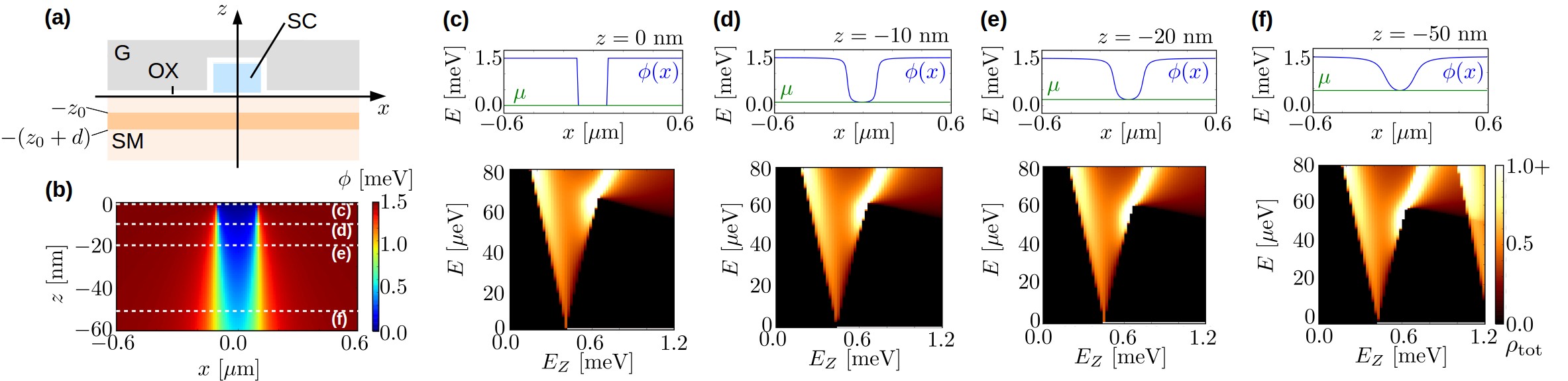
A more realistic modeling of the electrostatic potential is obtained by solving both the Schrödinger equation,
| (52) |
and the Poisson equation,
| (53) |
self-consistently. In Eq. (52), is the Hamiltonian describing in principle the entire device including the 2DEG heterostructure and the superconductor [Fig. 13(a)]. The Hamiltonian incorporates the effect of the electrostatic potential , which acts as a position-dependent shift of the electrochemical potential . The electrostatic potential is the solution of Eq. (53), in which is the vacuum permittivity, is the dielectric constant of the material (which can position-dependent) and is the charge distribution. The charge distribution, in turn, depends on the probability density associated with the electronic energy levels filled up to at zero temperature. Solving Eqs. (52) and (53) incorporates charging effects at the Hartree level.
In order to obtain MBSs with a large topological energy gap, the chemical potential is close to the bottom of the potential well Hell et al. (2017). Under this condition, the electron charge density in the 2DEG is rather small. In this case, one can ignore the effect of the electron density on the electrostatic potential as we argue next. Concretely, let us consider the case that the 2DEG under the superconductor is occupied only by a single mode due to the confinement in the and the direction [Fig. 13(a)]. Since the stripe length in the direction is much larger than all other length scales, the level spacing of modes in the direction is rather small. The electron density of states per length in the direction can thus approximated by that of infinite 1D system at zero temperature:
| (54) |
Neglecting superconductivity, we can set eV, the spin-orbit energy, and as in most of calculations. Using , we obtain
| (55) |
The charge density per volume is then given approximately by , assuming for simplicity that the charge is uniformly distributed over the cross section area of the 1D channel. This area is given by the stripe width in the direction and the width of the quantum well in the direction. Since , the electric field will mostly point along the direction and only at the edges of the stripe there will be a contribution in the direction. We can thus estimate the effect of the charge density on the potential in the quasi-1D channel by considering the potential difference across the quantum well in the direction [Fig. 13(a)]. Using that the electric field points in the direction, we can integrate Eq. (53) and obtain
assuming here that the dielectric constant is uniform. For the InAs / InGaAs / InAsAs heterostructures used in experiments in Ref. Shabani et al., 2016, the dielectric constants for all materials are about and we thus obtain
| (56) |
This is indeed negligible compared to gate-induced potentials on the meV scale. We thus set the charge density in the following.
When the charge density in the 2DEG is neglected and when a uniform dielectric constant is assumed, the gate-induced potential can be computed analytically for a split-gate structure as shown in Fig. 13(a). We will further make the assumption that the oxide layer thickness is negligible so that we may can employ Dirichlet boundary conditions and on the plane. Using von-Neumann boundary conditions for , , for the rest of the boundary, the solution to Eq. (53) reads Davies et al. (1995):
| (57) |
This gate-induced potential is shown in Fig. 13(b) and horizontal cuts at different distances below the gates are shown in the top panels of Fig. 13(c)–(f). In experimental setups, the 2DEG is about 10-20 nm below the semiconductor surface, for which the shape of the quantum well is still close to rectangular [Figs. 13(d) and (e)].
We used the more realistic gate potential (57) for different fixed values of to compute the total density of states [bottom panels of Fig. 13(c)–(f)] for otherwise the same parameters as in Fig. 3(d). We adjusted the chemical potential in all cases to the bottom of the potential well, i.e., . For and , we can see that there are only minor differences in the energy spectrum when using a rectangular or a smoothened potential profile [compare Figs. 13(d) and (e) to Fig. 13(c)]: The phase-transition point remains nearly unshifted and the topological energy gap is only slightly reduced.
A qualitative difference in the energy spectrum can only be seen for the
largest depth below the surface [bottom panel of Fig. 13(f)]. Here, a second Andreev bound state approaches zero
energy for large Zeeman energies. Such a state would probably also appear for
the other cases of smaller —— when increasing the Zeeman energy. The reason
why this state appears for lower Zeeman energies in the case of is probably that the confinement energy for higher-lying excited
states is reduced for the more smoothened potential profile. However, a single
MBS appears still in a broad regime of Zeeman energies. The case of is still relevant because it can be used to estimate the effect of
an oxide layer with a nonzero thickness. Our results show that even in this
case, one can expect that the results of the rectangular potential barrier
hold in the single-subband regime with only small modifications.
References
- Alicea (2012) J. Alicea, Rep. Prog. Phys. 75, 076501 (2012).
- Leijnse and Flensberg (2012) M. Leijnse and K. Flensberg, Semicond. Sci. Technol. 27, 124003 (2012).
- Beenakker (2013) C. W. J. Beenakker, Annu. Rev. Con. Mat. Phys. 4, 113 (2013).
- Stanescu and Tewari (2013) T. D. Stanescu and S. Tewari, J. Phys.: Condens. Matter 25, 233201 (2013).
- Bravyi and Kitaev (2002) S. Bravyi and A. Kitaev, Annals of Physics 298, 210 (2002).
- Bravyi and Kitaev (2005) S. Bravyi and A. Kitaev, Phys. Rev. A 71, 022316 (2005).
- Freedman et al. (2003) M. H. Freedman, A. Kitaev, M. J. Larsen, and Z. Wang, Bull. Amer. Math. Soc. 40, 31 (2003).
- Oreg et al. (2010) Y. Oreg, G. Refael, and F. von Oppen, Phys. Rev. Lett. 105, 177002 (2010).
- Sau et al. (2010a) J. D. Sau, R. M. Lutchyn, S. Tewari, and S. Das Sarma, Phys. Rev. Lett. 104, 040502 (2010a).
- Lutchyn et al. (2010) R. M. Lutchyn, J. D. Sau, and S. Das Sarma, Phys. Rev. Lett. 105, 077001 (2010).
- Alicea (2010) J. Alicea, Phys. Rev. B 81, 125318 (2010).
- Mourik et al. (2012) V. Mourik, K. Zuo, S. M. Frolov, S. R. Plissard, E. P. A. M. Bakkers, and L. P. Kouwenhoven, Science 336, 1003 (2012).
- Das et al. (2012) A. Das, Y. Ronen, Y. Most, Y. Oreg, M. Heiblum, and H. Shtrikman, Nat. Phys. 8, 887 (2012).
- Finck et al. (2013) A. D. K. Finck, D. J. Van Harlingen, P. K. Mohseni, K. Jung, and X. Li, Phys. Rev. Lett. 110, 126406 (2013).
- Rokhinson et al. (2012) L. P. Rokhinson, X. Liu, and J. K. Furdyna, Nat. Phys. 8, 795 (2012).
- Deng et al. (2012) M. T. Deng, C. L. Yu, G. Y. Huang, M. Larsson, P. Caroff, and H. Q. Xu, Nano Lett. 12, 6414 (2012).
- Albrecht et al. (2016) S. M. Albrecht, A. P. Higginbotham, M. Madsen, F. Kuemmeth, T. S. Jespersen, J. Nyg, P. Krogstrup, and C. M. Marcus, Nature 531, 206 (2016).
- Zhang et al. (2016) H. Zhang, Ö. Gül, S. Conesa-Boj, K. Zuo, V. Mourik, F. K. de Vries, J. van Veen, D. J. van Woerkom, M. P. Nowak, M. Wimmer, et al., arXiv preprint arXiv:1603.04069 (2016).
- Deng et al. (2016) M. T. Deng, S. Vaitiekenas, E. B. Hansen, J. Danon, M. Leijnse, K. Flensberg, J. Nygård, P. Krogstrup, and C. M. Marcus, Science 354, 1557 (2016).
- Williams et al. (2012) J. R. Williams, A. J. Bestwick, P. Gallagher, S. S. Hong, Y. Cui, A. S. Bleich, J. G. Analytis, I. R. Fisher, and D. Goldhaber-Gordon, Phys. Rev. Lett. 109, 056803 (2012).
- Nadj-Perge et al. (2014) S. Nadj-Perge, I. K. Drozdov, J. Li, H. Chen, S. Jeon, J. Seo, A. H. MacDonald, B. A. Bernevig, and A. Yazdani, Science 346, 602 (2014).
- Ruby et al. (2015) M. Ruby, F. Pientka, Y. Peng, F. von Oppen, B. W. Heinrich, and K. J. Franke, Phys. Rev. Lett. 115, 197204 (2015).
- Suominen et al. (2017) H. J. Suominen, M. Kjaergaard, A. R. Hamilton, J. Shabani, C. J. Palmstrøm, C. M. Marcus, and F. Nichele, arXiv preprint arXiv:1703.03699v1 (2017).
- Fu and Kane (2009) L. Fu and C. L. Kane, Phys. Rev. B 79, 161408 (2009).
- Benjamin and Pachos (2010) C. Benjamin and J. K. Pachos, Phys. Rev. B 81, 085101 (2010).
- Sun and Wu (2014) B. Y. Sun and M. W. Wu, New Journal of Physics 16, 073045 (2014).
- Ueda and Yokoyama (2014) A. Ueda and T. Yokoyama, Phys. Rev. B 90, 081405 (2014).
- Yamakage and M (2014) A. Yamakage and S. M, Physica E 55, 13 (2014), ISSN 1386-9477.
- Sau et al. (2015) J. D. Sau, B. Swingle, and S. Tewari, Phys. Rev. B 92, 020511 (2015).
- Rubbert and Akhmerov (2016) S. Rubbert and A. R. Akhmerov, Phys. Rev. B 94, 115430 (2016).
- Tripathi et al. (2016) K. M. Tripathi, S. Das, and S. Rao, Phys. Rev. Lett. 116, 166401 (2016).
- Fu (2010) L. Fu, Phys. Rev. Lett. 104, 056402 (2010).
- Aasen et al. (2016) D. Aasen, M. Hell, R. V. Mishmash, A. Higginbotham, J. Danon, M. Leijnse, T. S. Jespersen, J. A. Folk, C. M. Marcus, K. Flensberg, et al., Phys. Rev. X 6, 031016 (2016).
- Alicea et al. (2011) J. Alicea, Y. Oreg, G. Refael, F. von Oppen, and M. P. A. Fisher, Nat. Phys. 7, 412 (2011).
- Clarke et al. (2011) D. J. Clarke, J. D. Sau, and S. Tewari, Phys. Rev. B 84, 035120 (2011).
- Halperin et al. (2012) B. I. Halperin, Y. Oreg, A. Stern, G. Refael, J. Alicea, and F. von Oppen, Phys. Rev. B 85, 144501 (2012).
- Hyart et al. (2013) T. Hyart, B. van Heck, I. C. Fulga, M. Burrello, A. R. Akhmerov, and C. W. J. Beenakker, Phys. Rev. B 88, 035121 (2013).
- Hell et al. (2016) M. Hell, J. Danon, K. Flensberg, and M. Leijnse, Phys. Rev. B 94, 035424 (2016).
- Sau et al. (2011) J. D. Sau, D. J. Clarke, and S. Tewari, Phys. Rev. B 84, 094505 (2011).
- van Heck et al. (2012) B. van Heck, A. R. Akhmerov, F. Hassler, M. Burrello, and C. W. J. Beenakker, New Journal of Physics 14, 035019 (2012).
- Bonderson (2013) P. Bonderson, Phys. Rev. B 87, 035113 (2013).
- Vijay and Fu (2016) S. Vijay and L. Fu, Phys. Rev. B 94, 235446 (2016).
- Karzig et al. (2016) T. Karzig, C. Knapp, R. Lutchyn, P. Bonderson, M. Hastings, C. Nayak, J. Alicea, K. Flensberg, S. Plugge, Y. Oreg, et al., arXiv preprint arXiv:1610.05289 (2016).
- Shabani et al. (2016) J. Shabani, M. Kjaergaard, H. J. Suominen, Y. Kim, F. Nichele, K. Pakrouski, T. Stankevic, R. M. Lutchyn, P. Krogstrup, R. Feidenhans’l, et al., Phys. Rev. B 93, 155402 (2016).
- Schäpers (2001) T. Schäpers, Superconductor/semiconductor junctions, vol. 174 (Springer Science & Business Media, 2001).
- Chrestin and Merkt (1997) A. Chrestin and U. Merkt, Appl. Phys. Lett. 70, 3149 (1997).
- Chrestin et al. (1999) A. Chrestin, R. Kürsten, K. Biedermann, T. Matsuyama, and U. Merkt, Superlattices Microstruct. 25, 711 (1999).
- Takayanagi et al. (1995) H. Takayanagi, T. Akazaki, and J. Nitta, Phys. Rev. Lett. 75, 3533 (1995).
- Bauch et al. (2005) T. Bauch, E. Hürfeld, V. M. Krasnov, P. Delsing, H. Takayanagi, and T. Akazaki, Phys. Rev. B 71, 174502 (2005).
- Kjaergaard et al. (2016a) M. Kjaergaard, F. Nichele, H. Suominen, M. Nowak, M. Wimmer, A. Akhmerov, J. Folk, K. Flensberg, J. Shabani, C. Palmstrøm, et al., arXiv preprint arXiv:1603.01852 (2016a).
- Suominen et al. (2016) H. Suominen, J. Danon, M. Kjaergaard, K. Flensberg, J. Shabani, C. Palmstrøm, F. Nichele, and C. Marcus, arXiv preprint arXiv:1611.00190 (2016).
- Kjaergaard et al. (2016b) M. Kjaergaard, H. J. Suominen, M. P. Nowak, A. R. Akhmerov, C. J. Shabani, C. J. Palmstrøm, F. Nichele, and C. M. Marcus, arXiv preprint arXiv:1607.04164 (2016b).
- Hell et al. (2017) M. Hell, M. Leijnse, and K. Flensberg, Phys. Rev. Lett. 118, 107701 (2017).
- Pientka et al. (2016) F. Pientka, A. Keselman, E. Berg, A. Yacoby, A. Stern, and B. I. Halperin, arXiv preprint arXiv:1609.09482 (2016).
- Pedrocchi and DiVincenzo (2015) F. L. Pedrocchi and D. P. DiVincenzo, Phys. Rev. Lett. 115, 120402 (2015).
- Pedrocchi et al. (2015) F. L. Pedrocchi, N. E. Bonesteel, and D. P. DiVincenzo, Phys. Rev. B 92, 115441 (2015).
- Sau et al. (2010b) J. D. Sau, R. M. Lutchyn, S. Tewari, and S. Das Sarma, Phys. Rev. B 82, 094522 (2010b).
- Stanescu et al. (2010) T. D. Stanescu, J. D. Sau, R. M. Lutchyn, and S. Das Sarma, Phys. Rev. B 81, 241310 (2010).
- Danon and Flensberg (2015) J. Danon and K. Flensberg, Phys. Rev. B 91, 165425 (2015).
- van Heck et al. (2016) B. van Heck, R. M. Lutchyn, and L. I. Glazman, Phys. Rev. B 93, 235431 (2016).
- Ferry and Goodnick (1997) D. Ferry and S. M. Goodnick, Transport in nanostructures, vol. 6 (Cambridge University Press, 1997).
- Wimmer (2008) M. Wimmer, Ph. d. thesis, Univiersität Regensburg (2008).
- Plugge et al. (2017) S. Plugge, A. Rasmussen, A. Egger, and K. Flensberg, New Journal of Physics 19, 012001 (2017).
- Vuik et al. (2016) A. Vuik, D. Eeltink, A. Akhmerov, and M. Wimmer, New Journal of Physics 18, 033013 (2016).
- Kammhuber et al. (2017) J. Kammhuber, M. C. Cassidy, F. Pei, M. P. Nowak, A. Vuik, D. Car, S. R. Plissard, E. P. Bakkers, M. Wimmer, and L. P. Kouwenhoven, arXiv preprint arXiv:1701.06878 (2017).
- Davies et al. (1995) J. H. Davies, I. A. Larkin, and E. V. Sukhorukov, Journal of Applied Physics 77, 4504 (1995).
- Lutchyn et al. (2011) R. M. Lutchyn, T. D. Stanescu, and S. Das Sarma, Phys. Rev. Lett. 106, 127001 (2011).