Detection of charge density wave phase transitions at 1T-TaS2/GaAs interfaces
Abstract
The transition metal dichalcogenide 1T-TaS2 is well known to harbor a rich variety of charge density wave (CDW) distortions which are correlated with underlying lattice atom modulations. The long range CDW phases extend throughout the whole crystal and terminate with charge displacements at the crystal boundaries. Here we report on the transport properties and capacitance characteristics of the interface between freshly exfoliated flakes of 1T-TaS2 in intimate van der Waals contact with n-type GaAs substrates. The extracted barrier parameters (ideality, barrier height and built-in potential) experience pronounced changes across the Mott-CDW transition in the 1T-TaS2. The CDW-induced changes in barrier properties are well described by a bond polarization model which upon decreasing temperature gives rise to an increased potential drop across the interfacial region due to the localization of carriers and a decreased dielectric constant.
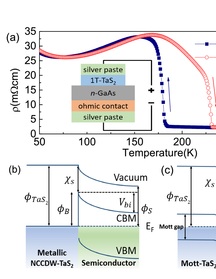
1T-TaS2, although simple in structure, embodies various collective electronic states, which have recently triggered intensive studybishop2008 ; yu2015 ; yoshida2015 ; vask2016 . Above 540 K, 1T-TaS2 is a normal metal with the Ta 5d band crossing the Fermi level. Upon cooling, it transforms into an incommensurate CDW (ICCDW) state, which then evolves into a near commensurate CDW (NCCDW) phase at 350 K. Below Tcc ( K), the transition temperature on cooling, a long range ordered commensurate CDW (CCDW) develops accompanied by a large resistance increase. The resistance drops back at Tcw ( K), the transition temperature on warming, as shown in Fig. 1(a). Since 1T-TaS2 is host to a rich variety of CDW phases, there has been widespread interest and success in controlling the transition between CDW states or even hidden metastable states with electric fields, voltage pulses or optical excitationsHoll2015 ; sto2014 ; do2015 . These studies not only facilitate the understanding of the correlation between these complex CDW phases in 1T-TaS2, but also imply promise for technological applications. Recently, memristors and oscillators based on 1T-TaS2 utilizing the first-order CDW phase transitions have been realizedyoshida2015 ; liu2016 .
Despite the intense effort in studying intrinsic single crystals, 1T-TaS2 based heterojunctions via integration with three-dimensional (3D) semiconductors have not been explored. Our strategy in addressing how 1T-TaS2 might ultimately be used in pure 2D electronic configurations is based on our previous discovery that exfoliated flakes of highly ordered pyrolytic graphite (HOPG) simply pressed against clean semiconductor substrates (Si, GaAs, 4H-SiC) display excellent Schottky barrier rectification effectstongay_apl . With the realization that the outermost layer, a single sheet of graphene, in contact with the semiconductor, played a major role in the formation of the Schottky barrier, it was a straightforward matter to produce similar results using 2D single layers of graphene rather than 3D flakestongay_prx . With the current explosion of interest in other van der Waals (vdW) crystals such as layered superconductors, topological insulators and transition metal dichalcogenides, interfacing 2D materials with 3D traditional semiconductors deserves attention and has achieved progress in both high performance devices and detailed device physics prototypes which require modification of the conventional models based on 3D materialsxu2016 .
In this letter we report on a similar strategy in an investigation of the electrical properties of 1T-TaS2 flakes in intimate contact with n-type GaAs substrates. The objective is to obtain a better understanding of the intricate physics at interfaces when long range ordered CDW phases are present in one of the electrodes, in this case the 1T-TaS2. When 1T-TaS2 crystalline flakes make intimate contacts to n-type GaAs, strong rectifying current density-voltage () characteristics persist from 100 K to 300 K. Both transport and capacitance measurements are sensitive to the CDW transition (CCDW-NCCDW) during cooling and warming cycles. We interpret our observations within the framework of the bond polarization model where the potential across the interfacial dipole is affected by the presence of CDW phases in 1T-TaS2. Our investigation incorporating charge density waves not only opens up an insightful perspective in understanding the physics at 2D/3D interfaces, but also accelerates the pace of device applications of such systems with first-order phase transitions.
A schematic diagram of a van der Waals junction is shown in the inset of Fig. 1(a). Commercially available n-type GaAs wafers with nominal cm-3 (Si) doping concentration were used. High quality ohmic contacts were made on the unpolished side with traditional recipes existing in the literaturegaas ; sze2006 . 1T-TaS2 thin flakes (10-50 µm thick) were mechanically exfoliated from 1T-TaS2 crystals and then transferred onto cleaned (100) GaAs wafers. For electrical contact, silver paste with an area ranging from 0.3 to 2 mm2 covered the top surface of the 1T-TaS2 electrode. We found that samples fabricated in ambient atmosphere or glove boxes containing inert gas showed similar electrical features, implying oxidation effects are not severe during our sample fabrication process (see supplementary material).
All the transport measurements were carried out inside a physical property measurement system (PPMS) using either a Keithley 2400 source meter or lock-in techniques. Hall effect measurement shows the doping concentration of our n-type GaAs to be cm-3 at room temperature. Three-terminal capacitance measurements using an HP 4284A LCR meter were performed on samples in a custom capacitance probe with a sensitivity of 0.1 pFtongay2009 .
We start with the ideal band alignment of 1T-TaS2/n-type GaAs junctions. Above Tcc during the cooling cycle, 1T-TaS2 is in the metallic state with an electron concentration ( 1022 cm-3)p2006 ; inda1980 , leading to Schottky like junctions when interfacing with GaAs, as shown in Fig. 1(b). Transport across such Schottky junctions is dominated by electrons and is well described by the thermionic-emission equation for the current density:
| (1) |
where is the total current equal to the product with the effective area , is the Richardson constant, is the temperature, is the zero bias Schottky barrier height, is the ideality factor indicating the contribution of thermionic-emission processes, and is the contact resistance. Complementary to transport, junction capacitance in the reverse bias region is given by
,
where is the effective sample area, is the built-in potential, is the ionized donor density, is the relative dielectric constant of the semiconductor and is the vacuum permittivity.
Compared to measurements, capacitance offers a more accurate band profile, but is insensitive to various transport channels.
When entering the Mott-CCDW state, 1T-TaS2 becomes a p-type semiconductor, with a Mott gap meV openinginda1980 ; cho2015 . Thus, 1T-TaS2 in the Mott-CCDW state will form pn heterojunctions with n-type GaAs. The corresponding band alignment is demonstrated in Fig. 1(c)you2013 . As for transport, tunneling current is affected as the density of states (DOS) profile changes on the 1T-TaS2 side. Holes also contribute to transport.
Junction capacitance still leads to an accurate measure of the built-in potential, which is given bysze2006 :
| (2) |
where is the effective acceptor density in 1T-TaS2. In contrast to Schottky barriers, the measured equals the sum of band bending on the 1T-TaS2 side and GaAs side, denoted by and respectively in Fig.1(c). Given that sze2006 , the band bending in 1T-TaS2 is still very small, since the carrier concentration of 1T-TaS2 in the Mott-CCDW state ( 1019 cm-3)inda1980 is much larger than that of GaAs ( 1016 cm-3) and the dielectric constant of both sides is similarbishop2008 .
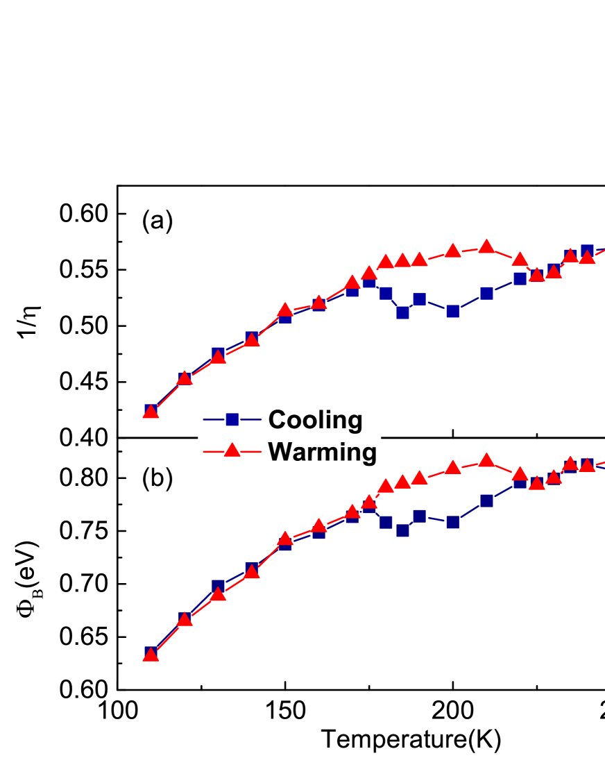
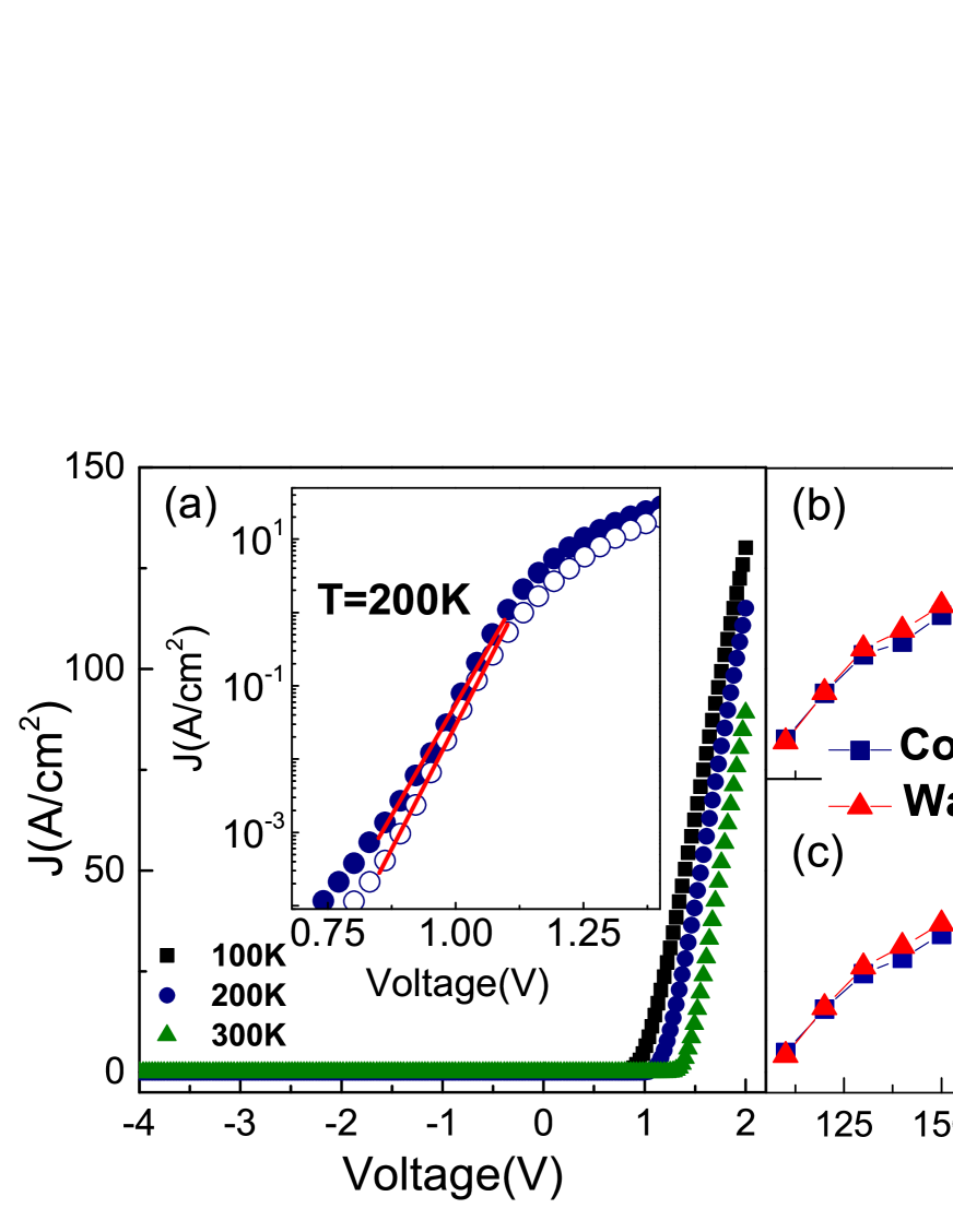
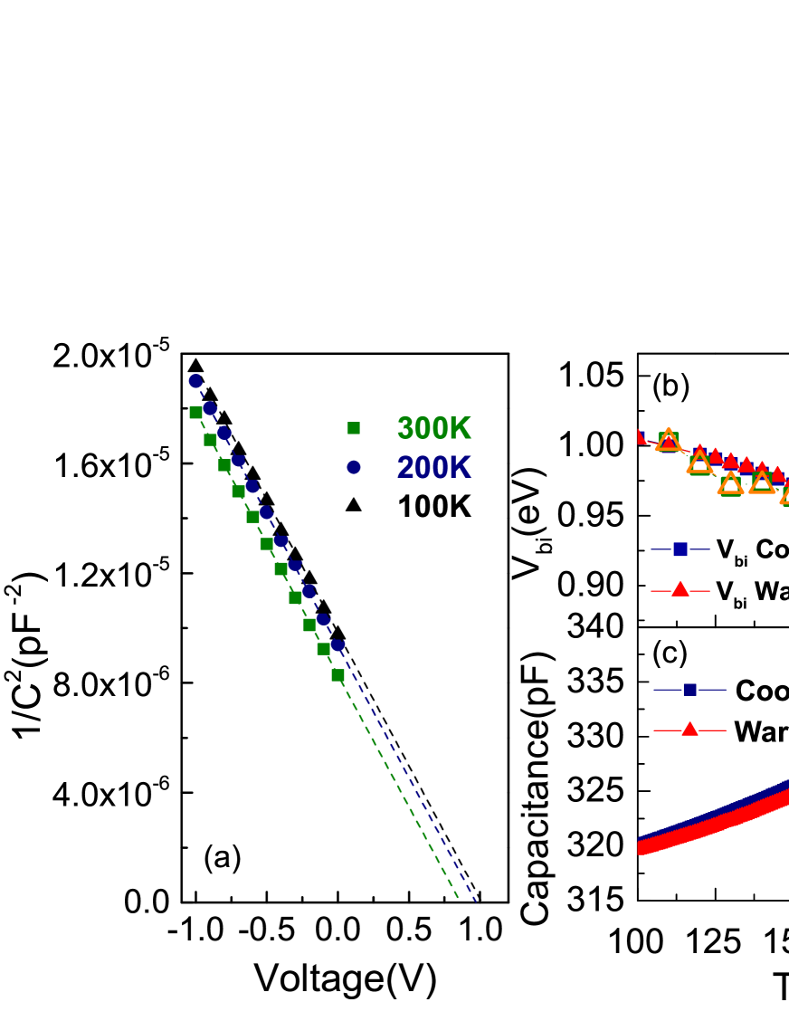
Fig. 2(a) shows the typical curves of a 1T-TaS2/GaAs junction below and above the transition temperature in the cooling cycle. 1T-TaS2 is defined as the positive side. All curves show a pronounced rectifying feature. The reduction of forward bias current density at low temperature is mainly due to the increasing contact resistance. To explore how CDW formation would affect the transport properties, we plot in the inset of Fig.2(a) the forward bias curves at 200 K, where almost the largest hysteresis of 1T-TaS2 single crystal resistivity takes place. A reduction of forward bias current is observed in the warming cycle.
In principle, transport data of 1T-TaS2/GaAs junctions cannot be fitted with a unified model across CDW phase transitions. However, the thermionic-emission process, although not the sole contribution, still plays an important role. Thus, analysis of curves based on the thermionic-emission equation
still suffices to reveal changes at the interface. The fitted is thus a physical parameter incorporating the most dominant transport mechanismsang2016 . As shown by the red dashed line in the inset of Fig. 2(a), typical data in the forward bias region displays over 2 decades of linearity on a semilogarithmic scale, enabling us to extract and .
As shown in Fig. 2(b), the ideality of 1T-TaS2/GaAs junctions generally increases with decreasing temperatures primarily due to the significant contribution of tunneling and thermally assisted tunneling at low temperaturespa1965 . When going through the NCCDW to Mott-CCDW transition, experiences a rapid drop (Fig. 2(b)), while, on the other hand, increases at Tcc (Fig. 2(c)). Our explanation is that with lowering temperature the Mott gap opens, thereby lowering the available density of states near the Fermi level and thus the tunneling current. Consequently, the contribution of thermionic process is more dominant, represented by a drop in concomitant with an increase of , both signifying an increased contribution of thermionic emission currentwe1991 . Although transport channels like hole diffusion and generation-recombination may exist with Mott gap opening, according to our data, their contribution is less significant than tunneling processes. The obvious hysteresis in both and demonstrates that the formation of the Mott-CCDW state indeed modifies the transport picture of 1T-TaS2/GaAs junctions.
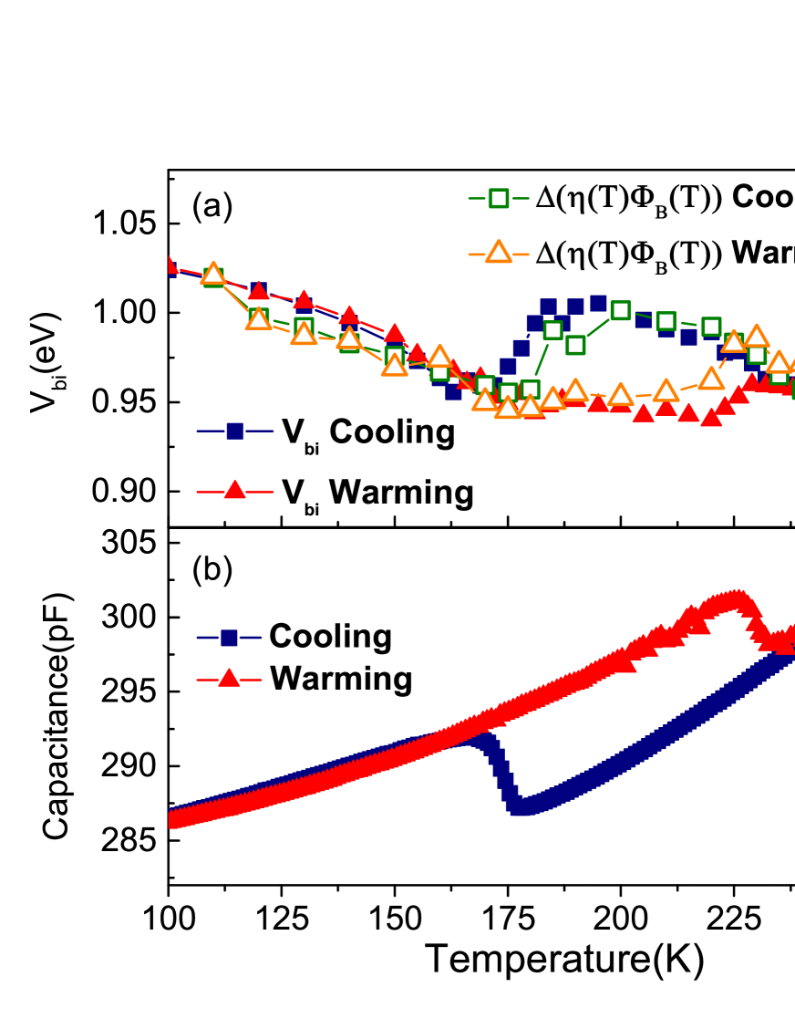
Capacitance reflects the flat band voltagewe1991 , giving a more accurate description of interface band alignment evolution across the CDW phase transition. The characteristic linear relationship between and is observed in our studied temperature range as shown in Fig. 3(a). Extrapolation of these data to the abscissa provides temperature-dependent as summarized in Fig. 3(b). For normal metal/n-type semiconductor junctions, as temperature decreases, Vbi keeps increasing, which is consistent with the work function of n-type extrinsic semiconductors which decreases when lowering the temperature. Our extracted Vbi values exhibit the same trend except the hysteresis and rapid change at the CDW transition temperatures. The measured Vbi drops by around 50 meV during cooling near 180 K and jumps back on warming near 230 K.
As previously reported, the product is an estimation of flat band voltageang2016 ; we1991 . We also plot as open symbols the -dependent product difference, , in Fig. 3(b) and find the same temperature dependence as V (solid symbols) obtained from capacitance measurements. This similarity suggests our transport and capacitance data are consistent with each other as shown previously for a variety of diodesang2016 ; we1991 . The abrupt decrease of is further confirmed by zero-bias capacitance temperature () measurement as shown Fig. 3(c). When entering the Mott-CCDW state, if no built-in potential (effective work function) variation takes place, the junction capacitance would slightly decrease as the band bending in 1T-TaS2 side results in two capacitors connected in series. However, the measured capacitance changes in the opposite way (i.e., increases), implying a decrease in , as predicted by Eq. 2. A similar picture applies when 1T-TaS2 changes back to the metallic state, with a jump of as long range CDW order is destroyed. We note that junctions fabricated in the glove box demonstrate similar hysteresis features in both transport parameters and capacitance data (see supplementary material).
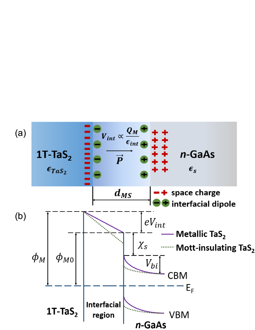
To explain our observed capacitance features, a detailed interfacial band alignment is needed. Considering the ideal metal-semiconductor (MS) interface, the Shottky-Mott rule applies, which predicts the room temperature barrier height to be 1.13 eV, given that the work function of 1T-TaS2 is 5.2eVshimada1994 and the electron affinity of GaAs is 4.07 eVsze2006 . However, based on our built-in potential, the average barrier height of 8 junctions at room temperature is 0.97 eV, indicating the necessity of considering Fermi level pinning (FLP) effect commonly observed in real MS interfacestung2001 . The most relevant mechanisms explaining FLP effect include metal-induced gap states (MIGS)metal-Si ; h1965 , defect induced gap states (DIGS)h1983 and bond polarizationtung2000 ; tung20012 . However, MIGS has been proven to be largely suppressed in van der Waals junctionssc2016 , while DIGS is closely correlated to the quality of 1T-TaS2 flakes and semiconductor wafers. We assume that the DIGS effect, although present, is small and cannot serve as the explanation for our observed features taking place right at Tcc and Tcw.
In the bond polarization model, as shown in Fig. 4(a), in addition to the formation of the space charge region, charge exchange also occurs between the topmost layer of metal and semiconductor when an intimate contact is formed. DFT calculations confirm such charge transfer in transition metal dichalcogenide based interfacessc2016 ; g2014 .
According to the bond polarization model, charge transfer between 1T-TaS2 and the semiconductor can be written as:
| (3) |
where is the band gap of semiconductor, is the work function of intrinsic 1T-TaS2, is the electron affinity of the semiconductor and is a parameter related to interfacial Coulomb interactiontung2014 . Since 1T-TaS2 has a large work function, the interfacial charge transfer would result in an additional dipole pointing from 1T-TaS2 to the semiconductor. Such an interfacial dipole, attached to 1T-TaS2, would modify the work function of 1T-TaS2 by l2003 , where , with the electric charge, the effective interface dielectric constant and representing the interfacial dipole strength with areal density and separation (3 Å)g2014 . Here we define the effective work function () of 1T-TaS2, which includes the interfacial region, as .
The measured built-in potential for both MS junctions and pn heterojunctions is given by the difference between work functions. One apparent explanation for our observed built-in potential drop in the cooling cycle takes into account the work function change of intrinsic 1T-TaS2, since n-type GaAs experiences no sudden change of the work function across the CDW phase transition. However, limited information about the 1T-TaS2 work function is available. Only Shimada claims that no noticeable change of 1T-TaS2 work function is observed across the CDW phase transitionshimada1994 ; shimadad . As is well known, the extraction of work function is always intricate and can even provide opposite results across phase transitionsyou2013 , which makes the intrinsic work function change argument less convincing.
Another more promising explanation addresses the change of interfacial potential across CDW phase transitions. Since the atomic displacement for 1T-TaS2 changes less than 7ro2011 , we do not expect a sudden change in the number of interfacial dipoles relying heavily on lattice mismatch. The only remaining variable , determining the potential drop across a given interfacial dipole strength, is a combination of dielectric constant of GaAs and 1T-TaS2. The dielectric constant of GaAs remains almost unchanged in the studied temperature range. Above Tcc during the cooling cycle, metallic 1T-TaS2 has a large dielectric constant. When entering the Mott-CCDW state, the dielectric constant of 1T-TaS2 becomes comparable to GaAs, consistent with a metal-insulator transitionbishop2008 . Such a dielectric constant drop leads to a larger interfacial potential drop as shown in Fig. 4(b), decreasing the effective work function of 1T-TaS2. Accordingly, the measured Vbi experiences a drop at Tcc and then jumps back at Tcw.
In summary, we have systematically studied the transport properties and capacitance characteristics of 1T-TaS2/n-type GaAs van der Waals heterojunction. The transport related parameters and are sensitive to the Mott-CCDW formation. We ascribe the transport picture modification to different tunneling contributions originating from a modified DOS profile. In addition, the built-in potential from measurement drops with the CCDW formation which is consistent with the concomitant changes in the zero-bias data. We explain the observed feature based on bond polarization model that localization of free carriers renders a larger potential drop across interfacial dipoles due to less effective screening. Such combination of exfoliated TMD materials with traditional semiconductors may bridge the gap between traditional MS interfaces and pure 2D material interfaces where large scale fabrication and ohmic contact remain as challenges and have implication for the next generation devices based on phase transition TMDs.
See supplementary material for the electrical measurements of a typical junction fabricated in the glove box containing argon.
The authors thank Haoming Jin, Jie Hou and Chris Samouce for assistance with sample preparation and the Nanoscale Research Facility at the University of Florida for access to rapid thermal annealing facilities. This work was supported by the National Science Foundation under the Division of Materials Research Grant No. DMR-1305783 (AFH) and the Department of Energy under Grant No. DE-FG02-86ER45268 (GRS).
References
- (1) B. Sipos, A. F. Kusmartseva, A. Akrap, H. Berger, L. Forró, and E. Tutiš, Nat. Mater. 7, 960 (2008).
- (2) Y. Yu, F. Yang, X. F. Lu, Y. J. Yan, Y.-H. Cho, L. Ma, X. Niu, S. Kim, Y.-W. Son, D. Feng, S. Li, S.-W. Cheong, X. H. Chen, and Y. Zhang, Nat. Nanotechnol. 10, 270 (2015).
- (3) M. Yoshida, R. Suzuki, Y. Zhang, M. Nakano, and Y. Iwasa, Sci. Adv. 1, e1500606 (2015).
- (4) I. Vaskivskyi, I. A. Mihailovic, S. Brazovskii, J. Gospodaric, T. Mertelj, D. Svetin, P. Sutar, and D. Mihailovic, Nat. Commun. 7, 11442 (2016).
- (5) M. J. Hollander, Y. Liu, W. J. Lu, L. J. Li, Y. P. Sun, J. A. Robinson, and S. Datta, Nano Lett. 15, 1861 (2015).
- (6) L. Stojchevska, I. Vaskivskyi, T. Mertelj, P. Kusar, D. Svetin, S. Brazovskii, and D. Mihailovic, Science 344, 177 (2014).
- (7) D. Cho, S. Cheon, K.-S. Kim, S.-H. Lee, Y.-H. Cho, S.-W. Cheong, and H. W. Yeom, Nat. Commun. 7, 10453 (2016).
- (8) G. Liu, B. Debnath, T.R. Pope, T.T. Salguero, R.K. Lake, and A.A. Balandin, Nat. Nanotechnol. 11, 845 (2016).
- (9) S. Tongay, T. Schumann, and A.F. Hebard, Appl. Phys. Lett. 95, 222103 (2009).
- (10) S. Tongay, M. Lemaitre, X. Miao, B.P. Gila, B.R. Appleton, and A.F. Hebard, Phys. Rev. X 2, 011002 (2012).
- (11) Y. Xu, C. Cheng, S. Du, J. Yang, B. Yu, J. Luo, W. Yin, E. Li, S. Dong, P. Ye, and X. Duan, ACS Nano 10, 4895 (2016).
- (12) S. M. Sze and K. K. Ng, Physics of semiconductor devices (Wiley, New York, 2006).
- (13) P.H Hao, L.C. Wang, F. Deng, S.S. Lau, and J.Y. Cheng, J. Appl. Phys. 79(8), 4211 (1996).
- (14) S. Tongay, A. F. Hebard, Y. Hikita, and H. Y. Hwang, Phys. Rev. B 80, 205324 (2009).
- (15) L. Perfetti, P. A. Loukakos, M. Lisowski, U. Bovensiepen, H. Berger, S. Biermann, P. S. Cornaglia, A. Georges, and M. Wolf, Phys. Rev. Lett. 97, 067402 (2006).
- (16) R. Inada, Y. Onuki, and S. Tanuma, Physica B + C 99, 188 (1980).
- (17) D. Cho, Y.-H Cho, S.-W. Cheong, K.-S. Kim, and H. W. Yeom, Phys. Rev. B 92, 085132 (2015).
- (18) Y. Zhou and S. Ramanathan, J. Appl. Phys. 113, 213703 (2013).
- (19) A. J. Li and A. F. Hebard, J. Phys. D: Appl. Phys. 49, 455101 (2016).
- (20) F.A. Padovani and G.G. Sumner, J. Appl. Phys. 36, 3744 (1965).
- (21) J.H. Werner and H.H. Güttler, J. Appl. Phys. 69, 1522 (1991).
- (22) T. Shimada, F. S. Ohuchi, and B. A. Parkinson, Jpn. J. Appl. Phys. 33, 2696 (1994).
- (23) R. Tung, Mater. Sci. Eng., R. 35, 1 (2001).
- (24) J. Tersoff, Physical Review Letters 52, 6 (1984).
- (25) V. Heine, Phys. Rev. 138, A1689 (1965).
- (26) H. Hasegawa and T. Sawada, Thin Solid Films 103, 119 (1983).
- (27) R. T. Tung, Phys. Rev. Lett. 84, 6078 (2000).
- (28) R. T. Tung, Phys. Rev. B 64, 205310 (2001).
- (29) Y. Liu, P. Stradins, and S.-H. Wei, Sci. Adv. 2, e1600069 (2016).
- (30) C. Gong, L. Colombo, R. M. Wallace, and K. J. Cho, Nano Lett. 14, 1714 (2014).
- (31) R. T. Tung, Appl. Phys. Rev. 1, 011304 (2014).
- (32) T. C. Leung, C. L. Kao, W. S. Su, Y. J. Feng, and C. T. Chan, Phys. Rev. B 68, 195408 (2003).
- (33) T. Shimada, Ph.D. Thesis, University of Tokyo, (1993).
- (34) K. Rossnagel, J. Phys.: Condens. Matter 23, 213001 (2011).
Supplemental information for Detection of charge density wave phase transitions at 1T-Tas2/GaAs interfaces
The electrical measurement data are shown for one typical 1T-TaS2/GaAs junction fabricated in the glove box containing argon. Transport parameters (Figure S 1) and capacitance data (Figure S 2) are consistent with the data of the sample fabricated in the ambient atmosphere which are presented in the main text. The clear hysteretic features in barrier parameters suggest that the CDW induced changes at the interface are robust and the surface degradation effect of 1T-TaS2 is small during our sample fabrication process.