In-plane Propagation of Light in Transition Metal Dichalcogenide Monolayers: Optical Selection Rules
Abstract
The optical selection rules for inter-band transitions in WSe2, WS2 and MoSe2 transition metal dichalcogenide monolayers are investigated by polarization-resolved photoluminescence experiments with a signal collection from the sample edge. These measurements reveal a strong polarization-dependence of the emission lines. We see clear signatures of the emitted light with the electric field oriented perpendicular to the monolayer plane, corresponding to an inter-band optical transition forbidden at normal incidence used in standard optical spectroscopy measurements. The experimental results are in agreement with the optical selection rules deduced from group theory analysis, highlighting the key role played by the different symmetries of the conduction and valence bands split by the spin-orbit interaction. These studies yield a direct determination on the bright-dark exciton splitting, for which we measure 40 meV and 55 meV for WSe2 and WS2 monolayer, respectively.
Two-dimensional crystals of transition metal dichalcogenides such as MX2 (M=Mo, W; X=S, Se, Te) are promising atomically flat semiconductors for applications in electronics and optoelectronics Butler et al. (2013); Geim and Grigorieva (2013); Mak et al. (2010); Splendiani et al. (2010); Wang et al. (2012). The optical properties of transition metal dichalcogenides (TMD) monolayers (MLs) are governed by very robust excitons with binding energy of the order of 500 meV He et al. (2014); Ugeda et al. (2014); Chernikov et al. (2014); Ye et al. (2014); Qiu et al. (2013); Ramasubramaniam (2012); Wang et al. (2015). The interplay between inversion symmetry breaking and strong spin-orbit coupling in these MLs also yields unique spin/valley properties Xiao et al. (2012); Sallen et al. (2012); Mak et al. (2012); Kioseoglou et al. (2012); Cao et al. (2012); Jones et al. (2013); Yang et al. (2015). Due to the two-dimensional (2D) character of the layered materials, the band-to-band transitions are predicted to be anisotropic for light propagating parallel to the plane of the ML. The insights gained from these type of experiments in III-V semiconductor quantum wells Weiner et al. (1985); Marzin et al. (1985) were crucial for designing optoelectronic devices. For 2D materials based on TMDs the light polarized perpendicular to the ML ( direction) should involve transitions with energies different from the transitions observed for in-plane polarized light Glazov et al. (2014); Echeverry et al. (2016). So far, however, optical spectroscopy measurements in TMD MLs have only been made for normal incidence for which the polarization is not accessible. Indeed the natural geometry in optical spectroscopy consists in exciting and collecting light from the top of the sample, with light wave-vectors perpendicular to the ML plane. In addition to the measurement of the predicted anisotropy of the interaction of light, optical experiments performed for light propagating parallel to the ML should bring precious information on the detailed band structure of these 2D materials. In particular, it allows for a straightforward determination of the energy difference between bright and dark excitons, for which a direct measurement is still lacking Zhang et al. (2015); Wang et al. (2015); Arora et al. (2015); Withers et al. (2015).
In this Letter we present the first measurements of the luminescence properties of TMD MLs for light propagating along the plane of the layer. In this geometry the electric field of the optical radiation can be either parallel or perpendicular to the ML. We measure the polarization-dependent emission properties of different TMD MLs for this in-plane optical excitation and detection geometry. For WSe2 and WS2 MLs, a new luminescence line emerges for the polarization perpendicular to the 2D material plane, corresponding to a -dipole transition. This transition is forbidden at normal incidence in linear optical spectroscopy because the electromagnetic field is transverse. Our measurements yield a direct determination of the bright-dark exciton splitting, in agreement with the selection rules deduced from group theory. We find 40 and 55 meV in WSe2 and WS2 MLs, respectively. For MoSe2 ML, no signature of the dark state is evidenced as a consequence of the very low population of the dark exciton states which lie at higher energy compared to the bright ones Kośmider et al. (2013); Echeverry et al. (2016); Kormanyos et al. (2015); Dery and Song (2015).
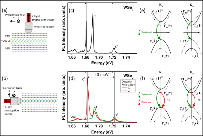
We have investigated MX2 MLs encapsulated in hexagonal boron nitride (hBN) and transferred onto an SiO2(90 nm)/Si substrate, see schematics in Fig. 1(a,b). The design of these samples is critical to the success of the experiment. It was shown recently that encapsulation of MX2 ML in high quality hBN results in very high quality samples where surface protection and substrate flatness yield very small photoluminescence (PL) or reflectivity linewidths, in the range meV at low temperature Wang et al. (2017); Ajayi et al. (2017); Cadiz et al. (2017); Manca et al. (2016). In the present investigation the narrow exciton lines will allow us to identify clearly transitions involving different bands for different polarizations of the light propagating in the ML plane. These van der Waals heterostructures are obtained by mechanical exfoliation of bulk MX2 (from 2D Semiconductors, USA) and hBN crystals Taniguchi and Watanabe (2007), following the fabrication technique detailed in Ref. Cadiz et al. (2017). The typical thickness of the hBN layers is nm and the in-plane size of the MX2 ML is m2. The samples are held on a cold finger in a closed-cycle cryostat. Two configurations for the microscope objective inside the cryostat are used for the excitation and collection of PL along or perpendicular to the ML plane, Fig. 1(a,b). Attocube X-Y-Z piezo-motors allow for positioning with nm resolution of the ML with respect to the microscope objective (numerical aperture NA) used for excitation and collection of luminescence. The ML is excited by a continuous wave green laser (2.33 eV). For WSe2 and MoSe2 MLs similar results have been obtained with He-Ne laser excitation (1.96 eV). The laser average power is about 50 W. The excitation laser and detection spot diameter is m. The PL signal is dispersed in a spectrometer and detected with a Si-CCD camera Wang et al. (2014). For the measurements from the edge of the sample, the ratio between the focused laser spot diameter and the thickness of the ML is smaller than 1000. Though challenging from the point of view of the required alignment accuracy this experiment can be successful as shown below thanks to (i) the very large absorption coefficient of the TMD ML for in-plane polarized light Li et al. (2014), (ii) the longer interaction length between the light and 2D material compared to normal incidence excitation configuration and (iii) the detection efficiency of our set-up, designed for studies of single photon emitters Belhadj et al. (2009).
Figure 1(c) presents the PL spectrum at K of the WSe2 ML in the standard configuration, i.e. propagation of light perpendicular to the ML. We observe clearly the peaks corresponding to the recombination of neutral exciton X0 ( eV), trion – charged exciton – T ( eV) and lower energy lines ( eV) usually attributed to localized excitons, in agreement with already published results Jones et al. (2015); Arora et al. (2015); Wang et al. (2015). For this geometry where the light is polarized in the ML plane, the detected neutral exciton luminescence X0 corresponds to the radiative recombination involving both conduction band (CB) and valence band (VB) in the valley and conduction band and valence band in the valley , see the green arrows in Fig. 1(e). Both transitions conserve the spin. In contrast the transitions in the -valley between the CB and VB with opposite spins ( CB and VB in the -valley) are optically forbidden for the in-plane polarized light. The energy difference between the corresponding dark exciton and the bright X0 depends both on the spin-orbit splitting in the conduction band and the short range part of the electron-hole exchange interaction, where is the energy difference between () CB and () in valley (). The calculations predict values of a few tens of meV for WSe2 ML Echeverry et al. (2016); Qiu et al. (2015).
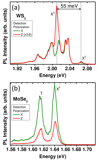
We present now the key results associated to the measurements from the edge of the sample, enabling the excitation and collection of the PL signal emitted with a wave-vector parallel to the ML, as schematically depicted in Fig. 1(b). The great advantage of this geometry is that it is suitable for measuring the interaction of the 2D material with light for both polarization directions, parallel to the plane of the ML – -polarized – as in Fig. 1(c) or perpendicular to it – -polarized. The optical selection rules, which depend intimately on the band structure of the ML and the exciton symmetry, can thus be revealed. In Fig. 1(d) the PL spectra of the WSe2 ML for both in-plane () and perpendicular () to the plane polarization are displayed. As expected the in-plane polarized PL spectrum (green line) is very similar to the normal incidence excitation/detection geometry shown in Fig. 1(c). As the polarization of the detected luminescence is identical, the same optical selection rules apply and we observe the three lines associated to neutral (X0), charged (T) and localized excitons. The detection energies of the lines are identical for both geometries but we note a larger broadening for excitation/detection from the sample edge resulting probably from the longer interaction length in the 2D material. Remarkably a new line labelled XD shows up in addition to the previous ones when the luminescence polarized perpendicular to the ML is detected, red line in Fig. 1(d). In agreement with the selection rules detailed below, this peak corresponds to the radiative recombination of excitons involving the transitions between the bottom () CB and topmost () VB in the valley (). We recall that these transitions are optically forbidden (“dark excitons”) for in-plane polarized light, in agreement with the -polarized spectrum in Fig. 1(d). As a consequence the energy difference between X0 and XD in Fig. 1(d) is a direct measurement of the bright-dark exciton splitting. We find meV in WSe2. Figure 2(a) presents the result of the same experiment performed on WS2 ML at K. Again when the luminescence polarized perpendicular to the ML is detected, a new line (XD) shows up and we measure a bright-dark exciton splitting energy of 55 meV. These accurate measurements will be a key element to improve the parametrization of ab-initio calculations of the band structure Echeverry et al. (2016).
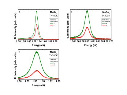
Finally we perform the same investigation for a MoSe2 ML both at K and 300 K. No spectral signature of the XD line is observed in MoSe2 ML in Fig. 2(b) at low temperature and in Fig. S4 of the supplement sup at higher temperature. This behavior is compatible with our current understanding of the MoSe2 ML band structure. Though the exact value of is still unknown, both theoretical and experimental investigations predict that the dark exciton lie at higher energy compared to the bright one (in contrast to WSe2 and WS2 ML) Zhang et al. (2015); Wang et al. (2015); Arora et al. (2015); Withers et al. (2015). The main reason is the change of sign of the spin-orbit splitting in the conduction band between these different materials Kośmider et al. (2013). Very recent investigations based on the coupling of the excitons to transverse high magnetic fields (tens of teslas) Zhang et al. (2017); Molas et al. (2016), or surface plasmon polaritons Zhou et al. (2017) inferred similar bright-dark exciton splitting energies. We emphasize that our measurements are based on the intrinsic properties of the MLs and do not require any external perturbation in addition to the light. For the sake of completeness we have also investigated the dependence of the PL spectra detected from the edge of the sample as a function of the polarization of the excitation laser propagating along the ML plane. In the previous experiments, Figs. 1, 2, the laser was polarized in the ML plane along -axis. As expected, the PL intensity for the -polarized excitation laser is reduced (see Fig. S2 in sup ). However the relative oscillator strength of the -polarized and -polarized transition at a given energy can not be deduced from these measurements because of the non-resonant energy of the excitation laser where the selection rules are difficult to determine.
The conclusions drawn from the experimental results are confirmed by the group theory analysis of the selection rules. Let us recall that the orbital Bloch functions of the valence band in and transform according to the same scalar representation (notations of Ref. Kos ) of point group relevant at the points. The conduction band orbital Bloch functions transform according to and respectively. As a result, the spinor representations for the valence band are () and (), while for the conduction band, Fig. 1(e), they are
| (1a) | |||
| (1b) | |||
Interband optical excitation gives rise to the electron-hole pairs bound into excitons by the Coulomb interaction. The excitonic states with envelope function detected in our experiments transform according to the representations , where is the representation of the conduction band state and is the representation of the empty valence band state. Note that the hole state is the time-reversed of the unoccupied valence band state therefore the conjugation of is needed Glazov et al. (2015). The exciton state is optically active in a given polarization if contains the irreducible representation according to which the corresponding polarization vector transforms. As a consequence for the optically active excitons must contain , i.e., the in-plane polarization, or , -polarization. Hereafter we consider only vertical optical transitions and obtain for possible symmetries of the exciton
| (2a) | ||||
| (2b) | ||||
The basic functions of and irreducible representations transform as , respectively. Hence, Eq. (2a) describes the excitons active in the and polarizations at the normal incidence of radiation, see green arrows in Fig. 1(e,f). Here the electron spin in the course of the interband transition is conserved and the polarization of the PL is determined by the orbital character of the Bloch functions. By contrast, the transitions involving opposite spins for the conduction and valence band states are forbidden at the normal incidence because they couple with the light of -polarization, i.e., normal to the ML plane. These transitions are depicted by red arrows in Fig. 1(f). This is in agreement with the measurement of the additional line XD which is -polarized in Figs. 1(d) and 2(a) for WSe2 and WS2 ML respectively.
A deeper insight into the symmetry of excitonic states can be obtained by considering the irreducible representations of the point group relevant for the overall symmetry of the ML. Such an analysis allows one to study the mixing of excitons in different valleys. The results in the supplement sup demonstrate that out of two -polarized states, and one linear combination with equal weights is active in the -polarization and can be attributed to the XD line, while another one is forbidden.
As these transitions require spin-orbit interaction to induce spin mixing, their oscillator strengths are expected to be much weaker than the one for in-plane polarized light. It can be qualitatively described by taking into account the interaction of the upper valence bands and with remote bands with different orbital character and opposite spin orientations, see supplement sup . Recent density functional theory calculations performed at the GW level combined with Bethe-Salpeter equation for excitons predict that the out-of plane contribution is times smaller than the in-plane one Echeverry et al. (2016). Though our experiments clearly evidence both transitions, the measured PL intensities cannot be used for the accurate determination of the relative ratio of the oscillator strengths since the non-resonant excitation results in an unknown populations of the exciton states X0 and XD. Particularly, the assumption of a thermodynamical equilibrium between the X0 and XD is questionable considering the very short radiative lifetime of X0 Korn et al. (2011); Lagarde et al. (2014); Robert et al. (2016). Further investigations based, e.g., on absorption or photocurrent measurements performed with strictly resonant excitation are required.
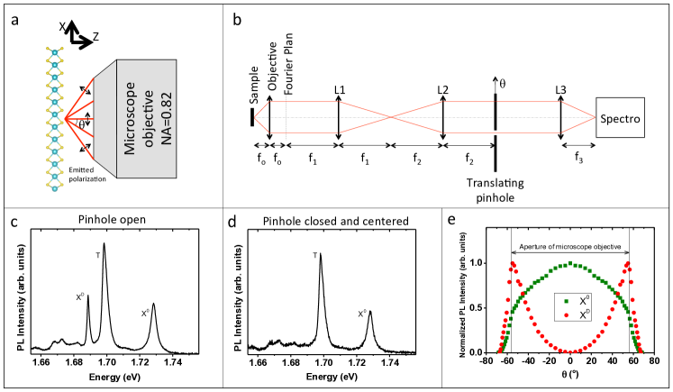
Finally we note in Fig. 1(c) a PL line at the energy XD (1.68 eV) for normal incidence excitation/detection where the optical selection rules dictate that this transition should be optically forbidden. The observation of this line is, actually, not surprising: First it can have a purely geometric origin. As we use a microscope objective with high NA, the electric field vector at the focal tail has a significant component along the -axis which enables excitation/detection of the XD transition even at the normal incidence. The percentage of the -mode to the total intensity was estimated to be in a similar study performed in GaAs quantum wells Schardt et al. (2006). Second, a lowering of the symmetry of the 2D crystal due to local strain or ripples can induce a small mixing between bright and dark excitons, yielding the observation of the XD component even for normal incidence Bayer et al. (2002). The same arguments can explain the observation of both X0 and T lines for the out-of-plane polarization in Figs. 1(d), 2, where the luminescence is collected from the edge of the ML. To elucidate the origin we note that by detecting only the central part of the PL spot for normal incidence excitation/detection, the XD line totally vanishes confirming that the -component is located off-axis only, see Fig. S5 of supplement sup . This demonstrates that the XD line observed in Fig. 1(c) is simply linked to the geometry of the experiment based on a microscope objective with a large numerical aperture.
In conclusion the first measurements of the optical properties of transition metal dichalcogenide MLs for light propagating along the plane are reported and discussed in terms of optically allowed and forbidden transitions depending on the light polarization and propagation direction. These experiments reveal important features of the band structure of these atomically-thin semiconductors. In addition to their importance for the knowledge of the band structure and excitonic properties in TMDC MLs, these experiments pave the way to the investigation of waveguides heterostructures and devices based on 2D materials.
Acknowledgements. We thank ERC Grant No. 306719, ITN Spin-NANO Marie Sklodowska-Curie grant agreement No 676108, ANR MoS2ValleyControl, Programme Investissements d Avenir ANR-11-IDEX-0002-02, reference ANR-10- LABX-0037-NEXT for financial support and Laboratoire International Associe ILNACS CNRS-Ioffe. X.M. also acknowledges the Institut Universitaire de France. K.W. and T.T. acknowledge support from the Elemental Strategy Initiative conducted by the MEXT, Japan and JSPS KAKENHI Grant Numbers JP26248061, JP15K21722 and JP25106006. M.M.G. is grateful to the RFBR, Dynasty Foundation and RF President grant MD-1555.2017.2 for partial support.
References
- Butler et al. (2013) Sheneve Z. Butler, Shawna M. Hollen, Linyou Cao, Yi Cui, Jay A. Gupta, Humberto R. Gutiérrez, Tony F. Heinz, Seung Sae Hong, Jiaxing Huang, Ariel F. Ismach, Ezekiel Johnston-Halperin, Masaru Kuno, Vladimir V. Plashnitsa, Richard D. Robinson, Rodney S. Ruoff, Sayeef Salahuddin, Jie Shan, Li Shi, Michael G. Spencer, Mauricio Terrones, Wolfgang Windl, and Joshua E. Goldberger, “Progress, challenges, and opportunities in two-dimensional materials beyond graphene,” ACS Nano 7, 2898–2926 (2013).
- Geim and Grigorieva (2013) A. K. Geim and I. V. Grigorieva, “Van der waals heterostructures,” Nature 499, 419—425 (2013).
- Mak et al. (2010) Kin Fai Mak, Changgu Lee, James Hone, Jie Shan, and Tony F. Heinz, “Atomically thin : A new direct-gap semiconductor,” Phys. Rev. Lett. 105, 136805 (2010).
- Splendiani et al. (2010) Andrea Splendiani, Liang Sun, Yuanbo Zhang, Tianshu Li, Jonghwan Kim, Chi-Yung Chim, Giulia Galli, and Feng Wang, “Emerging photoluminescence in monolayer mos2,” Nano Letters 10, 1271 (2010).
- Wang et al. (2012) Qing Hua Wang, Kourosh Kalantar-Zadeh, Andras Kis, Jonathan N Coleman, and Michael S Strano, “Electronics and optoelectronics of two-dimensional transition metal dichalcogenides,” Nature nanotechnology 7, 699–712 (2012).
- He et al. (2014) Keliang He, Nardeep Kumar, Liang Zhao, Zefang Wang, Kin Fai Mak, Hui Zhao, and Jie Shan, “Tightly bound excitons in monolayer ,” Phys. Rev. Lett. 113, 026803 (2014).
- Ugeda et al. (2014) M. M. Ugeda, A. J. Bradley, S.-F. Shi, F. H. da Jornada, Y. Zhang, D. Y. Qiu, S.-K. Mo, Z. Hussain, Z.-X. Shen, F. Wang, S. G. Louie, and M. F. Crommie, “Observation of giant bandgap renormalization and excitonic effects in a monolayer transition metal dichalcogenide semiconductor,” Nature Materials 13, 1091–1095 (2014).
- Chernikov et al. (2014) Alexey Chernikov, Timothy C. Berkelbach, Heather M. Hill, Albert Rigosi, Yilei Li, Ozgur Burak Aslan, David R. Reichman, Mark S. Hybertsen, and Tony F. Heinz, “Exciton binding energy and nonhydrogenic rydberg series in monolayer ,” Phys. Rev. Lett. 113, 076802 (2014).
- Ye et al. (2014) Z. Ye, T. Cao, K. O’Brien, H. Zhu, X. Yin, Y. Wang, S. G. Louie, and X. Zhang, “Probing Excitonic Dark States in Single-layer Tungsten Disulfide,” Nature 513, 214–218 (2014).
- Qiu et al. (2013) Diana Y. Qiu, Felipe H. da Jornada, and Steven G. Louie, “Optical spectrum of mos2: Many-body effects and diversity of exciton states,” Phys. Rev. Lett. 111, 216805 (2013).
- Ramasubramaniam (2012) Ashwin Ramasubramaniam, “Large excitonic effects in monolayers of molybdenum and tungsten dichalcogenides,” Phys. Rev. B 86, 115409 (2012).
- Wang et al. (2015) G. Wang, X. Marie, I. Gerber, T. Amand, D. Lagarde, L. Bouet, M. Vidal, A. Balocchi, and B. Urbaszek, “Giant enhancement of the optical second-harmonic emission of monolayers by laser excitation at exciton resonances,” Phys. Rev. Lett. 114, 097403 (2015).
- Xiao et al. (2012) Di Xiao, Gui-Bin Liu, Wanxiang Feng, Xiaodong Xu, and Wang Yao, “Coupled spin and valley physics in monolayers of and other group-vi dichalcogenides,” Phys. Rev. Lett. 108, 196802 (2012).
- Sallen et al. (2012) G. Sallen, L. Bouet, X. Marie, G. Wang, C. R. Zhu, W. P. Han, Y. Lu, P. H. Tan, T. Amand, B. L. Liu, and B. Urbaszek, “Robust optical emission polarization in mos2 monolayers through selective valley excitation,” Phys. Rev. B 86, 081301 (2012).
- Mak et al. (2012) Kin Fai Mak, Keliang He, Jie Shan, and Tony F. Heinz, “Control of valley polarization in monolayer by optical helicity,” Nat. Nanotechnol. 7, 494 (2012).
- Kioseoglou et al. (2012) G. Kioseoglou, A. T. Hanbicki, M. Currie, A. L. Friedman, D. Gunlycke, and B. T. Jonker, “Valley polarization and intervalley scattering in monolayer mos[sub 2],” Applied Physics Letters 101, 221907 (2012).
- Cao et al. (2012) Ting Cao, Gang Wang, Wenpeng Han, Huiqui Ye, Chuanrui Zhu, Junren Shi, Qian Niu, Pingheng Tan, Enge Wang, Baoli Liu, and Ji Feng, “Valley-selective circular dichroism in ,” Nature Communications 3, 887 (2012).
- Jones et al. (2013) Aaron M. Jones, Hongyi Yu, Nirmal J. Ghimire, Sanfeng Wu, Grant Aivazian, Jason S. Ross, Bo Zhao, Jiaqiang Yan, David G. Mandrus, Di Xiao, Wang Yao, and Xiaodong Xu, “Optical generation of excitonic valley coherence in monolayer wse2,” Nat. Nanotechnol. 8, 634–638 (2013).
- Yang et al. (2015) Luyi Yang, Nikolai A Sinitsyn, Weibing Chen, Jiangtan Yuan, Jing Zhang, Jun Lou, and Scott A Crooker, “Long-lived nanosecond spin relaxation and spin coherence of electrons in monolayer mos2 and ws2,” Nature Physics 11, 830–834 (2015).
- Weiner et al. (1985) J. S. Weiner, D. S. Chemla, D. A. B. Miller, H. A. Haus, A. C. Gossard, W. Wiegmann, and C. A. Burrus, “Highly anisotropic optical properties of single quantum well waveguides,” Applied Physics Letters 47, 664–667 (1985).
- Marzin et al. (1985) J.-Y. Marzin, M. N. Charasse, and B. Sermage, “Optical investigation of a new type of valence-band configuration in as-gaas strained superlattices,” Phys. Rev. B 31, 8298–8301 (1985).
- Glazov et al. (2014) M. M. Glazov, T. Amand, X. Marie, D. Lagarde, L. Bouet, and B. Urbaszek, “Exciton fine structure and spin decoherence in monolayers of transition metal dichalcogenides,” Phys. Rev. B 89, 201302 (2014).
- Echeverry et al. (2016) J. P. Echeverry, B. Urbaszek, T. Amand, X. Marie, and I. C. Gerber, “Splitting between bright and dark excitons in transition metal dichalcogenide monolayers,” Phys. Rev. B 93, 121107 (2016).
- Zhang et al. (2015) Xiao-Xiao Zhang, Yumeng You, Shu Yang Frank Zhao, and Tony F. Heinz, “Experimental evidence for dark excitons in monolayer ,” Phys. Rev. Lett. 115, 257403 (2015).
- Wang et al. (2015) G. Wang, C. Robert, A. Suslu, B. Chen, S. Yang, S. Alamdari, I. C. Gerber, T. Amand, X. Marie, S. Tongay, and B. Urbaszek, “Spin-orbit engineering in transition metal dichalcogenide alloy monolayers,” Nature Comms. , 10110 (2015).
- Arora et al. (2015) Ashish Arora, Maciej Koperski, Karol Nogajewski, Jacques Marcus, Clement Faugeras, and Marek Potemski, “Excitonic resonances in thin films of wse2: from monolayer to bulk material,” Nanoscale 7, 10421–10429 (2015).
- Withers et al. (2015) F. Withers, O. Del Pozo-Zamudio, S. Schwarz, S. Dufferwiel, P. M. Walker, T. Godde, A. P. Rooney, A. Gholinia, C. R. Woods, P. Blake, S. J. Haigh, K. Watanabe, T. Taniguchi, I. L. Aleiner, A. K. Geim, V. I. Fal???ko, A. I. Tartakovskii, and K. S. Novoselov, “Wse2 light-emitting tunneling transistors with enhanced brightness at room temperature,” Nano Letters 15, 8223–8228 (2015), pMID: 26555037, http://dx.doi.org/10.1021/acs.nanolett.5b03740 .
- Kośmider et al. (2013) K. Kośmider, J. W. González, and J. Fernández-Rossier, “Large spin splitting in the conduction band of transition metal dichalcogenide monolayers,” Phys. Rev. B 88, 245436 (2013).
- Kormanyos et al. (2015) A. Kormanyos, G. Burkard, M. Gmitra, J. Fabian, V. Zolyomi, N. D. Drummond, and V. Fal’ko, “k.p theory for two-dimensional transition metal dichalcogenide semiconductors,” 2D Materials 2, 022001 (2015).
- Dery and Song (2015) Hanan Dery and Yang Song, “Polarization analysis of excitons in monolayer and bilayer transition-metal dichalcogenides,” Phys. Rev. B 92, 125431 (2015).
- Wang et al. (2017) Zefang Wang, Liang Zhao, Kin Fai Mak, and Jie Shan, “Probing the spin-polarized electronic band structure in monolayer transition metal dichalcogenides by optical spectroscopy,” Nano Letters 17, 740–746 (2017), pMID: 28103668, http://dx.doi.org/10.1021/acs.nanolett.6b03855 .
- Ajayi et al. (2017) O. A. Ajayi, J. V. Ardelean, G. D. Shepard, J. Wang, A. Antony, T. Taniguchi, K. Watanabe, T. F. Heinz, S. Strauf, X.-Y. Zhu, and J. C. Hone, “Approaching the Intrinsic Photoluminescence Linewidth in Transition Metal Dichalcogenide Monolayers,” ArXiv e-prints (2017), arXiv:1702.05857 [cond-mat.mtrl-sci] .
- Cadiz et al. (2017) F. Cadiz, E. Courtade, C. Robert, G. Wang, Y. Shen, H. Cai, T. Taniguchi, K. Watanabe, H. Carrere, D. Lagarde, M. Manca, T. Amand, P. Renucci, S. Tongay, X. Marie, and B. Urbaszek, “Excitonic linewidth approaching the homogeneous limit in MoS2 based van der Waals heterostructures : accessing spin-valley dynamics,” ArXiv e-prints (2017), arXiv:1702.00323 [cond-mat.mtrl-sci] .
- Manca et al. (2016) M Manca, M M Glazov, C Robert, F Cadiz, T Taniguchi, K Watanabe, E Courtade, T Amand, P Renucci, X Marie, G Wang, and B Urbaszek, “Enabling valley selective exciton scattering in monolayer wse2 through upconversion,” ArXiv , 1701.05800 (2016).
- Taniguchi and Watanabe (2007) T. Taniguchi and K. Watanabe, “Synthesis of high-purity boron nitride single crystals under high pressure by using ba-bn solvent,” Journal of Crystal Growth 303, 525 – 529 (2007).
- Wang et al. (2014) G. Wang, L. Bouet, D. Lagarde, M. Vidal, A. Balocchi, T. Amand, X. Marie, and B. Urbaszek, “Valley dynamics probed through charged and neutral exciton emission in monolayer ,” Phys. Rev. B 90, 075413 (2014).
- Li et al. (2014) Yilei Li, Alexey Chernikov, Xian Zhang, Albert Rigosi, Heather M. Hill, Arend M. van der Zande, Daniel A. Chenet, En-Min Shih, James Hone, and Tony F. Heinz, “Measurement of the optical dielectric function of monolayer transition-metal dichalcogenides: , , , and ,” Phys. Rev. B 90, 205422 (2014).
- Belhadj et al. (2009) Thomas Belhadj, Claire-Marie Simon, Thierry Amand, Pierre Renucci, Beatrice Chatel, Olivier Krebs, Aristide Lemaître, Paul Voisin, Xavier Marie, and Bernhard Urbaszek, “Controlling the polarization eigenstate of a quantum dot exciton with light,” Phys. Rev. Lett. 103, 086601 (2009).
- Jones et al. (2015) Aaron M Jones, Hongyi Yu, John R Schaibley, Jiaqiang Yan, David G Mandrus, Takashi Taniguchi, Kenji Watanabe, Hanan Dery, Wang Yao, and Xiaodong Xu, “Excitonic luminescence upconversion in a two-dimensional semiconductor,” Nature Physics (2015).
- Qiu et al. (2015) Diana Y. Qiu, Ting Cao, and Steven G. Louie, “Nonanalyticity, valley quantum phases, and lightlike exciton dispersion in monolayer transition metal dichalcogenides: Theory and first-principles calculations,” Phys. Rev. Lett. 115, 176801 (2015).
- (41) See Supplementary Material which contains additional experimental data and detailed group-theory and effective Hamiltonian analysis.
- Zhang et al. (2017) X Zhang, T Cao, Z Lu, Y Lin, F Zhan, Y Wang, Z Li, J C Hone, J A Robinson, D Smirnov, S G Louie, and T F Heinz, “Magnetic brightening and control of dark excitons in monolayer wse 2,” ArXiv , 1612.03558 (2017).
- Molas et al. (2016) M R Molas, C Faugeras, A O Slobodeniuk, K Nogajewski, M Bartos, D M Basko, and M Potemski, “Brightening of dark excitons in monolayers of semiconducting transition metal dichalcogenides,” ArXiv:1612.02867 (2016).
- Zhou et al. (2017) Y. Zhou, G. Scuri, D. S. Wild, A. A. High, A. Dibos, L. A. Jauregui, C. Shu, K. de Greve, K. Pistunova, A. Joe, T. Taniguchi, K. Watanabe, P. Kim, M. D. Lukin, and H. Park, “Probing dark excitons in atomically thin semiconductors via near-field coupling to surface plasmon polaritons,” ArXiv e-prints (2017), arXiv:1701.05938 [cond-mat.mes-hall] .
- (45) G. F. Koster, J. O. Dimmock, G. Wheeler, R. G. Satz, Properties of thirty-two point groups (M.I.T. Press, Cambridge, Massachusetts USA) 1963.
- Glazov et al. (2015) M. M. Glazov, E. L. Ivchenko, G. Wang, T. Amand, X. Marie, B. Urbaszek, and B. L. Liu, “Spin and valley dynamics of excitons in transition metal dichalcogenide monolayers,” physica status solidi (b) 252, 2349–2362 (2015).
- Korn et al. (2011) T. Korn, S. Heydrich, M. Hirmer, J. Schmutzler, and C. Schüller, “Low-temperature photocarrier dynamics in monolayer ,” Applied Physics Letters 99, 102109 (2011).
- Lagarde et al. (2014) D. Lagarde, L. Bouet, X. Marie, C. R. Zhu, B. L. Liu, T. Amand, P. H. Tan, and B. Urbaszek, “Carrier and polarization dynamics in monolayer mos2,” Phys. Rev. Lett. 112, 047401 (2014).
- Robert et al. (2016) C. Robert, D. Lagarde, F. Cadiz, G. Wang, B. Lassagne, T. Amand, A. Balocchi, P. Renucci, S. Tongay, B. Urbaszek, and X. Marie, “Exciton radiative lifetime in transition metal dichalcogenide monolayers,” Phys. Rev. B 93, 205423 (2016).
- Schardt et al. (2006) M. Schardt, A. Winkler, G. Rurimo, M. Hanson, D. Driscoll, S. Quabis, S. Malzer, G. Leuchs, G.H. Döhler, and A.C. Gossard, “Te- and tm-polarization-resolved spectroscopy on quantum wells under normal incidence,” Physica E: Low-dimensional Systems and Nanostructures 32, 241 – 244 (2006), proceedings of the 12th International Conference on Modulated Semiconductor StructuresProceedings of the 12th International Conference on Modulated Semiconductor Structures.
- Bayer et al. (2002) M. Bayer, G. Ortner, O. Stern, A. Kuther, A. A. Gorbunov, A. Forchel, P. Hawrylak, S. Fafard, K. Hinzer, T. L. Reinecke, S. N. Walck, J. P. Reithmaier, F. Klopf, and F. Schäfer, “Fine structure of neutral and charged excitons in self-assembled in(ga)as/(al)gaas quantum dots,” Phys. Rev. B 65, 195315 (2002).
SI Supplemental material
SI.1 Extended group theoretical analysis
The analysis presented in the main text is based on the representations of the point symmetry group relevant for the single valley of the TMD ML. It is instructive to analyse the symmetry of the excitonic states in terms of irreducible representations of the point symmetry group relevant for the TMD ML as a whole. Making use of Ref. Kos we establish the following compatibility of the irreducible representations of these two point groups
| (3a) | |||
| (3b) | |||
| (3c) | |||
| (3d) | |||
Note that the different irreducible representations relevant for the Kramers-degenerate states from the valleys and join in the point symmetry group. Note that these representations are self-conjugate.
The excitons formed in the course of optical transitions involving topmost valence band and the top conduction subband, e.g., vertical spin-conserving transitions, Fig. 1(e,f) of the main text and Fig. S1, transform according to the reducible representation
| (4) |
The in-plane components of the vector transform according to the irreducible representation resulting in the optical activity of the excitons denoted by green arrows in Fig. 1(e,f) of the main text. Two remaining optical transitions where the electron from the top conduction subband recombines with the unoccupied state in the other valley are forbidden.
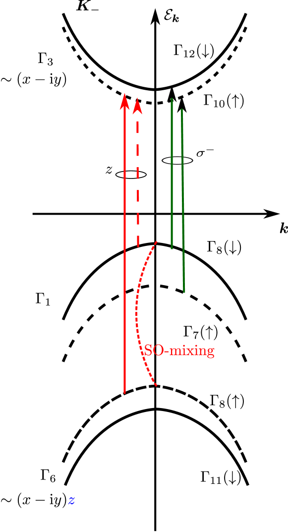
Let us now consider the excitons formed in the course of optical transitions involving the bottom conduction subband, e.g, vertical transitions with antiparallel conduction and valence band states, Fig. 1(f) of the main text and Fig. S1. We have
| (5) |
The -component of a vector transforms according to the irreducible representation. The states transforming according to the correspond to intervalley transitions activated with symmetric () phonon or due to the localization of the exciton on axially-symmetric defect potential Wang et al. (2015). We are interested in two remaining states transforming according to the irreducible representations and , respectively. These states are the linear combinations of the excitons formed in the course of vertical transitions between the states with opposite spins in the and valley. One of the states () is forbidden and another one () is allowed in -polarization as depicted in Fig. 1(f) of the main text by red arrows.
SI.2 Spin-orbit mixing of bands
The origin of the interband transitions without electron spin conservation is the spin-orbit interaction induced band mixing Pikus et al. (1988); Kormanyos et al. (2015). To illustrate the effect we consider the mixing of the topmost valence band and the remote valence band ( in the notations of Ref. Kormanyos et al. (2015)) whose orbital Bloch functions transform at the points as
| (6a) | |||||
| (6b) | |||||
Here and in what follows we use the irreducible representations of point group and omit the superscript denoting the group. The orbital Bloch functions are odd at the horizontal reflection unlike the even Bloch states of and involved in the exciton mixing Glazov et al. (2017), while at the operations which do not involve these functions transform like the conduction band Bloch functions. With account for spin the remote valence band gives rise to the following spin subbands:
| (7a) | |||
| (7b) | |||
| (7c) | |||
| (7d) | |||
Hence, in each valley there are deep valence band states which transform according to the same representations as the valence band top, but with reversed spins, see Fig. S1 for illustration of the states in the valley.
The Bloch functions of the top valence band, [], and the remote band, [], at the [] valley transform according to the same irreducible representation of the point group, therefore, these states are mixed, in general. The origin of the mixing is the atomic spin-orbit coupling in the form of
where and are the orbital and spin operators. For example, the state transforms as the state with the total angular momentum -component, , which is exactly the same as the -component of the topmost valence band state in the same valley, transforming as the function with . Within the effective Hamiltonian method the valence band top wavefunction in valleys can be presented as
| (8a) | |||
| (8b) |
In the first order perturbation theory one has
| (9) |
where is the spin-orbit mixing matrix elements and are the corresponding band edges. Due to the admixture, Eqs. (8), (9), the transition in polarization becomes possible between the valence and conduction band states with opposite spin orientations, see red dashed arrow in Fig. S1: This is because the transition between the admixed state and the conduction band state is possible in polarization and the spins of the admixed state and the conduction band state are parallel. The ratio of the oscillator strengths (radiative dampings) of the “dark” exciton in the polarization and of the “bright” exciton in the in-plane polarization can be estimated as
| (10) |
where is the interband () electric dipole matrix element in the polarization and is the interband () electric dipole moment matrix element in the in-plane polarization and we neglected the difference of effective masses in the different spin subbands which may affect the exciton envelope functions. Assuming and putting eV we obtain, for in the range of meV, the damping ratio in the range of . The density functional theory calculations gives in reasonable agreement with the crude estimate above Echeverry et al. (2016). We note that additive contribution to the mixing and the optical transitions is provided by the spin-orbit coupling with remote conduction band states. The parameters of these remote bands are not well established therefore the estimate Eq. (10) can serve as a criterion to improve the parameterizations of the effective Hamiltonian models.
SI.3 Additional experimental data
Figure S2 displays the photoluminescence spectra of WSe2 in different plarization configurations together with a polar plot of intensity of XD transition for fixed excitation and varied detection polarization.
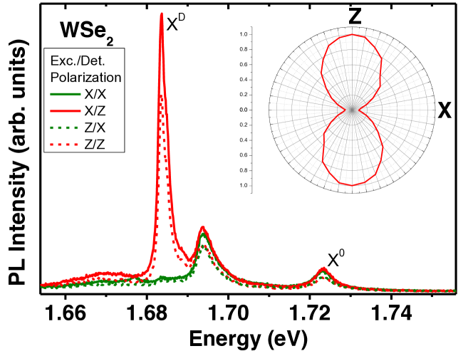
Figure S3 presents the intensities of emission of neutral (X0), charged (T), ”Dark” (XD) and localized (Loc.) excitons as a function of excitation power.
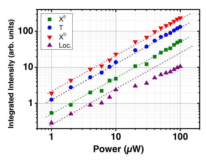
Figure S4 shows the photoluminescence spectrum of the MoSe2 monolayer at different temperatures.
SI.4 Spatial analysis of the PL
In Fig 1c of the main text, we showed that the XD transition at 1.68 eV is visible even for excitation and detection from the surface of the WS2 ML. This may be surprising at the first sight because the light propagation vector is along the -axis in this configuration so that the XD transition (which is -polarized) should not be visible. We show here that this is due to our large numerical aperture microscope objective. Fig. S5(a) sketches the detection configuration: Because of the large numerical aperture, light with an in-plane wave-vector component can be detected on the edge of the objective aperture. To confirm this situation we selectively filter the emitted light in angle by imaging the Fourier plan of the microscope objective [lenses L1 and L2 of Fig. S5(b)] and by placing a pinhole on this image. Translating the pinhole selects the angle of detection. Figure S5(c) shows the PL spectrum when the pinhole is opened, the configuration is thus the same as in Fig. 1(c) of the main text where both X0 and XD transitions are visible. When the pinhole is centered and almost closed, Fig. S5(d), only light with out-of-plane wavevector is detected. Consequently the XD transition is absent. In Fig. S5(e), we plot the intensities of both X0 and XD transitions as a function of the emitted angle . It clearly show that XD transition is only visible for large whereas the X0 is maximum for .
References
- (1) G. F. Koster, J. O. Dimmock, G. Wheeler, R. G. Satz, Properties of thirty-two point groups (M.I.T. Press, Cambridge, Massachusetts USA) 1963.
- Wang et al. (2015) G Wang, L Bouet, M M Glazov, T Amand, E L Ivchenko, E Palleau, X Marie, and B Urbaszek, “Magneto-optics in transition metal diselenide monolayers,” 2D Materials 2, 034002 (2015).
- Pikus et al. (1988) G.E. Pikus, V.A. Maruschak, and A.N. Titkov, “Spin splitting of energy-bands and spin relaxation of carriers in cubic III-V crystals,” Sov. Phys. Semicond. 22, 115 (1988).
- Kormanyos et al. (2015) A. Kormanyos, G. Burkard, M. Gmitra, J. Fabian, V. Zolyomi, N. D. Drummond, and V. Fal’ko, “k.p theory for two-dimensional transition metal dichalcogenide semiconductors,” 2D Materials 2, 022001 (2015).
- Glazov et al. (2017) M. M. Glazov, L. E. Golub, G. Wang, X. Marie, T. Amand, and B. Urbaszek, “Intrinsic exciton-state mixing and nonlinear optical properties in transition metal dichalcogenide monolayers,” Phys. Rev. B 95, 035311 (2017).
- Echeverry et al. (2016) J. P. Echeverry, B. Urbaszek, T. Amand, X. Marie, and I. C. Gerber, “Splitting between bright and dark excitons in transition metal dichalcogenide monolayers,” Phys. Rev. B 93, 121107 (2016).