Charged grain boundaries and carrier recombination in polycrystalline thin film solar cells
Abstract
We present analytical relations for the dark recombination current of a junction with positively charged columnar grain boundaries in the high defect density regime. We consider two defect state configurations relevant for positively charged grain boundaries: a single donor state and a continuum of both acceptors and donors. Compared to a continuum of acceptor+donor states, or to the previously studied single acceptor+donor state, the grain boundary recombination of a single donor state is suppressed by orders of magnitude. We show numerically that superposition holds near the open-circuit voltage , so that our dark relations determine for a given short circuit current . We finally explicitly show how depends on the these two grain boundary defect state configurations.
I Introduction
Polycrystalline photovoltaics have seen substantial increases in power conversion efficiency in recent years, exceeding the 20 % mark Green et al. (2017). Many of these advancements are due to improvements in light management, and have resulted in a short-circuit current density at 95 % of its theoretical maximum in CdTe Geisthardt et al. (2015). However, there remains substantial room for improvement in the open-circuit voltage ; the current record value of 850 mV in CdTe is only 76 % of its theoretical maximum Geisthardt et al. (2015). Despite the impressive progress in thin film photovoltaics, fundamental questions regarding the role of grain boundaries persist. For example, the relatively low efficiency of single crystal CdTe has led some to suggest that grain boundaries are beneficial to photovoltaic performance Jiang et al. (2004); Visoly-Fisher et al. (2006), while numerical simulations typically indicate that this is not the case Gloeckler et al. (2005); Taretto and Rau (2008); Rau et al. (2009); Troni et al. (2013). There are multiple reasons for the uncertainty regarding grain boundaries: experimentally, grain boundaries are difficult to independently control and measure, and theoretically there is not a simple analytical model which fully captures the physics of grain boundaries’ impact on photovoltaic performance.
Two recent reports Zhao et al. (2016); Burst et al. (2016) on single cyrstal CdTe solar cells showed open-circuit voltages above 1 V, indicating that grain boundaries are a primary source of losses due to recombination. This finding has renewed the impetus to understand and mitigate the impact of grain boundaries on . Most previous theoretical works in this direction have consisted of numerical simulations Gloeckler et al. (2005); Taretto and Rau (2008); Rau et al. (2009); Troni et al. (2013); Kanevce et al. (2017). Alternately, analytical models offer a concise, quantitative description of system behavior while providing further insight.
In light of the need for improved understanding of grain boundaries’ impact on , we recently developed an analytical description of dark grain boundary recombination current, with the primary result of a simple relation between grain boundary properties and Gaury and Haney (2016). Some details of the grain boundary model in this previous work are rather particular: we assumed that the grain boundary defect states consist of a donor and an acceptor at the same energy (so-called negative U-center). This assumption has been used in previous studies Edmiston et al. (1996); Taretto and Rau (2008) and is a simple way for the grain boundary to exhibit Fermi level pinning. However, the performance of polycrystalline photovoltaics like CdTe and Cu(In,Ga)Se2 depends critically on the grain boundary defect chemistry Rudmann et al. (2004); Kumar and Rao (2014). An adequately general model should therefore accommodate varied defect spectra.
In this work, we generalize our previous analysis to consider other grain boundary defect configurations. We provide closed form expressions and physical descriptions relating grain boundary properties to . Because a majority of experimental works provide evidence for positively charged grain boundaries in CdTe Yoon et al. (2013); Moutinho et al. (2010); Tuteja et al. (2016a), we restrict our attention to positively charged defects: a single donor defect and a continuum of donor and acceptor defects. We found that generalizing the grain boundary defect configurations necessitated a clearer and more general formulation of the model assumptions given in Ref. Gaury and Haney, 2016. The scope of this analysis is limited to grains with interior electrostatically similar to the unperturbed (i.e. grain boundary free) junction, and materials with large intragrain hole mobility (on the order of which is consistent with single crystal CdTe Sellin et al. (2005); Duenow et al. (2014)). To provide specific context, we present much of our analysis in terms of material parameters related to CdTe solar cells. However, our analysis is not material-specific, and applies to any material which conforms to the assumptions we make.
There are qualitative similarities between the behavior of the single donor+acceptor considered in Ref. Gaury and Haney, 2016 and the single donor and continuum cases studied here. In all cases, there are three regimes of qualitatively distinct behavior, which can roughly be classified according to the grain boundary core type: -type, -type, or neither (the latter case applies at high applied voltages, where both electron and hole densities vary with voltage). The full explicit form of the grain boundary dark current is shown in Table 1 for all defect configurations. An important new finding in this work is that compared to a continuum of acceptor+donor states, or to the previously studied single acceptor+donor state, the grain boundary recombination of a single donor state is suppressed by orders of magnitude.
This article is structured as follows. We begin with a description of the physical model for the grain boundary, encompassing both the single donor case and the continuum of gap states in Sec. II. We summarize the equilibrium properties of the grain boundary and our assumptions for analyzing the out-of-equilibrium problem in Sec. III. We present the charge transport and associated grain boundary dark current for the single donor state in Sec. IV, and for the continuum of gap states in Sec. V. We end the article with Sec. VI where we discuss the implications of our analysis on the open-circuit voltage of an illuminated junction. Finally, we examine the differences between the various configurations of the gap states considered in the paper.
| Grain boundary dark current: | |||||||
|---|---|---|---|---|---|---|---|
| Defect(s) | Param. | -type | -type | high-recombination | |||
| single D | n | ||||||
| N | |||||||
| S | |||||||
|
|
|
||||||
| single A+D | n | ||||||
| N | |||||||
| S | |||||||
|
|
|
||||||
| Continuum A+D | n | ||||||
| N | |||||||
| S | |||||||
|
|
|
||||||
II Physical model of the grain boundary
Our model system is depicted in Fig. 1(a): a junction of width and length with a grain boundary perpendicular to the junction. We use periodic boundary conditions in the -direction so that the system describes a closed grain of width ( in our numerical calculations). We assume selective contacts so that the majority (minority) carrier surface recombination velocity is infinite (zero), which implies that the electron (hole) current vanishes at (). We define as the position where electron and hole concentrations are equal in the grain interior. As stated in the introduction we focus on positively charged grain boundaries, which require screening by nearby negative charges (free electrons or ionized acceptor dopants) to conserve the device electroneutrality. The consequences of the screening on the electrostatics surrounding the grain boundary depend on the statistics of the gap levels, the defect density of states, and on the grain interior type (-type or -type region). For example, a -type material will develop an electric field around the grain boundary to repel free holes from the grain boundary core, creating a depleted region around it. Because of the absence of holes, this region has a negative charge compensating the positive charge of the defect, as shown in Fig. 1(b). Electroneutrality determines the spatial extent of this depleted region: the net charge (grain boundary charge plus depleted charge) of the ensemble grain boundary/depletion region is zero.
The consequence of the aforementioned electric field on the local energy landscape can be seen on a band structure plot across the grain boundary, as shown in Fig. 1(c). The electric field leads to the bending of the conduction and valence bands, leading to a built-in potential around the grain boundary. Depending on materials parameters and the extent of band bending, the grain boundary core may undergo type inversion with respect to the grain interior. Each grain boundary type has different carrier transport properties under nonequilibrium conditions. In this work we consider both inverted and non-inverted grain boundaries.
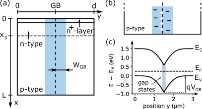
The grain boundary is modeled as a two-dimensional plane with various concentrations of donor and acceptor gap states. The grain boundary defect charge density reads
| (1) |
where () is a two-dimensional density of donor (acceptor) states per energy unit. The occupancies of each donor/acceptor state (indicated by the index ) is Shockley and Read (1952)
| (2) |
where () is the electron (hole) carrier density at the grain boundary, () is the electron (hole) surface recombination velocity, and are
| (3) | ||||
| (4) |
where is a defect energy level calculated from the valence band edge, () is the conduction (valence) band effective density of states, is the material bandgap, is the Boltzmann constant and is the temperature. The parameters and are related to the electron and hole capture cross sections by , where is the thermal velocity. In this work we vary with fixed ; this corresponds to varying accordingly. Note that at thermal equilibrium Eq. (2) reduces to the Fermi-Dirac distribution, and is independent of the recombination velocity parameters. In this case the occupancies of donor and acceptor states at energy are equal, which we denote by where .
In this work we restrict the scope of Eq. (1) to two cases of interest for positively charged grain boundaries. First, we focus on a single donor state at : , where is a two-dimensional defect density (units of ). Denoting , the grain boundary charge reads
| (5) |
Our second case, a continuum of gap states, is based on the observation that a wide variety of states populate the band gap of polycrystalline thin film materials Johnson et al. (2005); Krasikov and Sankin (2017). In the absence of precise knowledge of electronic defect structure for these materials, we consider a continuum of uniform densities of acceptor and donor states in the gap: , . is the ratio of acceptor to donor densities of states. For this case we use to denote the neutral energy level of the distribution of states: the grain boundary charge is zero when the gap states are filled to this level Rohderick (1978). If the Fermi level is above (below) , the grain boundary core develops a negative (positive) charge. At thermal equilibrium, the continuum of gap states can therefore be mapped onto an effective single defect level positioned at energy . The defect charge is then
| (6) |
where is now the effective occupancy of the effective single donor+acceptor defect state . This latter case was studied in detail in Ref. Gaury and Haney, 2016. This mapping from a continuum of donor+acceptor states to a single donor+acceptor state is valid for values of such that the densities of donor and acceptor states remain commensurate 111We will restrict to the interval . In the large defect density limit (specified below) we find that .
We consider large defect densities of states such that . We show in Appendix A that the critical defect density for this condition to be satisfied is
| (7) |
for the single donor state, and
| (8) |
for the continuum of acceptor and donor states. For material parameters typical of CdTe, Eq. (7) is on the order of for , and Eq. (8) ranges from to for .
III Equilibrium properties and assumptions away from equilibrium
III.1 Equilibrium properties
We first provide an expression for the equilibrium built-in potential in terms of the defect occupancy . In both single donor and continuum defect cases, the absence of recombination at thermal equilibrium gives the equilibrium carrier densities along the grain boundary 222The general net capture rate for electrons at the grain boundary core is . At thermal equilibrium this rate is zero which gives Eq. (9). The same reasoning applies for holes and leads to Eq. (10).
| (9) | ||||
| (10) |
We take the energy reference at the valence band edge in the grain interior of the -type material, as shown in Fig. 1(c). With this reference, the distance between the Fermi level and the conduction band at the grain boundary core is . This result determines another form of the equilibrium electron density at the grain boundary core, . Equating this form with Eq. (9) leads to the equilibrium grain boundary built-in potential
| (11) |
We next consider the determination of the equilibrium defect state occupancy . The value of is determined by electroneutrality: the grain boundary charge must be compensated by the charge of the surrounding depletion region. The depletion region width surrounding the grain boundary in the -type region is as shown in Fig. 1 (the schematic neglects the modification of the grain boundary built-in potential in the junction depletion region). For the donor case, the electroneutrality requirement leads to the following equation for :
| (12) |
where . In general Eq. (12) must be solved numerically for . Since no closed form of is available, we present our results in terms of the variable . Note that as , and the built-in potential of Eq. (11) diverges logarithmically. In practice, realistic values of are well below this diverging limit, so this issue can be safely ignored. In the continuum defect case, for the assumed large value of . In this case, Eq. (11) reduces to the previously studied single donor+acceptor case of Ref. Gaury and Haney, 2016.
III.2 Assumptions in the nonequilibrium analysis
A direct analytical solution for the full two-dimensional problem is not feasible. To make analytical progress, we split the two-dimensional system into two one-dimensional sub-systems: the grain boundary core where electrons are electrostatically confined Gloeckler et al. (2005); Gaury and Haney (2016); Tuteja et al. (2016b), and the grain interior (grain boundary free junction) where a solution is known. Our approach relies on approximations (or assumptions) which connect these two problems, and render the continuity-Poisson equations along the grain boundary core analytically tractable. In this section we state our assumptions and sketch out the subsequent solution procedures.
One blanket assumption is that the hole quasi-Fermi level is approximately flat across and along the grain boundary. This is valid because the hole current along the grain boundary is negligible (electrons carry the current along the grain boundary), while in the grain interior holes are majority carriers. We provide a criterion restricting the validity of this assumption in Appendix B. We find that for typical material parameters of CdTe, this assumption is generally valid for intragrain hole mobilities on the order of .
The next assumption is that the grain boundary charge does not change with voltage. This is justified by the limit of high defect density of states . This assumption is crucial as it enables us to relate the electrostatic potential to the quasi-Fermi levels without the Poisson equation. We denote the nonequilibrium defect occupancy with , which replaces in Eqs. (5) and (6) for systems out of equilibrium. is an integral of Eq. (2) and depends on the nonequilibrium carrier densities. Fixing the grain boundary charge to its equilibrium value results in assuming . The relative sizes of the terms in Eq. (2) delineate three regimes of different behavior:
- “-type” grain boundary
-
In this case, the defect occupancy is determined by the electron carrier density at the grain boundary. remains fixed by maintaining a constant distance between electron quasi-Fermi level and (actual or effective) . We further assume that the electron quasi-Fermi level is relatively flat and equal to its bulk value. This is valid because the high electron density in the grain boundary core enables high currents with relatively small quasi-Fermi level gradients. Together with the assumption of the relatively flat hole quasi-Fermi level, the densities and recombination are easily determined.
- “-type” grain boundary
-
In this case, the occupancy of the defect state(s) is determined by the hole carrier density at the grain boundary. remains fixed by maintaining a constant distance between the hole quasi-Fermi level and (actual or effective) . Because the electron density is small at the grain boundary core, the electron quasi-Fermi level develops gradients to drive the electron current along the grain boundary. In this case we must solve a one-dimensional diffusion equation for the electron density to obtain the carrier densities and recombination.
- High recombination
-
For sufficiently large applied voltages, the electron and hole carrier densities are the largest terms in the expression for and determine the defect occupancy. In the donor case, maintaining leads to the following relation between electron and hole density:
(13) In the continuum case, the occupancy of the acceptor and donor states are constrained to ensure that . Because is now an integral of the acceptor and donor occupancies, a simple relation like Eq. (13) does not exist. We show in Sec. V.3 that leads to the relation:
(14) where the density ratio varies weakly with voltage. In this high-recombination regime, Eq. (13) or Eq. (14) together with the assumption of flat hole quasi-Fermi level leads to a one-dimensional drift-diffusion equation for electrons confined to the grain boundary. Solving this equation leads to the carrier densities and recombination.
A final assumption which applies for all of our analysis is that the depletion regions of grain boundaries do not overlap, i.e. grain sizes are greater than . In other words, we assume that the electrostatic potential of the grain interior is the same as that of a grain boundary free junction. This assumption is necessary because we need a priori knowledge of the solution in the bulk in order to construct the solution along the grain boundary. For a doping density this requirement implies . The average grain size in CdTe thin films (excluding twin boundaries) was recently Moseley et al. (2015) found to be .
IV Grain boundary dark current of a single donor defect state
We begin with the case of a single donor state in the gap of the absorber material. The grain boundary charge is proportional to (see Eq. (5)). In the limit of large defect density of states, the electroneutrality of the grain boundary is satisfied when the defect level is fully occupied: . In the -region () the large concentration of electrons satisfies this requirement without the need for modifying the electrostatics around the grain boundary. In the -region, however, the resulting built-in potential around the grain boundary is given by Eq. (11)
| (15) |
Because of the logarithm term and , the Fermi level is not pinned to .
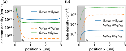
We now derive analytical expressions for the dark recombination current at the grain boundary. We support the physical descriptions with numerically computed carrier densities along the grain boundary presented in Fig. 2. The absence of modification of the electrostatics in the -region results in a recombination similar to the grain interior of the junction depletion region: the recombination is determined by the hole density (minority carrier density) which decreases sharply for , as shown in Fig. 2(b). In what follows we therefore neglect the contribution of this part of the grain boundary to the total recombination, and focus on carrier densities and recombination for . The general expression for the grain boundary recombination current reads
| (16) |
where is the length of the grain boundary. is the recombination at the grain boundary and has the Schockley-Read-Hall form
| (17) |
where is the intrinsic carrier density and we dropped the “donor” superscript for the recombination velocities. and are given by Eqs. (3) and (4) evaluated at .
As discussed in Sec. III, under nonequilibrium conditions we assume that the grain boundary carrier densities evolve while keeping the level occupancy equal to its thermal equilibrium value . Using this assumption and comparing the relative sizes of the terms in the nonequilibrium level occupancy Eq. (2) leads to three regimes of interest for the grain boundary dark current. We next analyze these regimes individually.
IV.1 Grain boundary recombination for
We first consider , also called “-type” regime. As discussed in Sec. III, for this case remains fixed by keeping constant. Equivalently, replaces in Eq. (15)Gaury and Haney (2016). In the grain interior of the -region, the increase of voltage shifts the electron quasi-Fermi level from the valence band by an amount . The electron current transverse to the grain boundary is small compared to the longitudinal one. So despite the low electron density in the grain interior, the gradient of across the grain boundary driving the transverse current is small and can be neglected. Assuming that is flat across the grain boundary, the built-in potential also varies with :
| (18) |
where is the equilibrium Fermi level. Equation (18) shows that the grain boundary built-in potential decreases linearly with voltage for . This is shown in Fig. 3(b). The reduction of the barrier allows holes of the grain interior to flow toward the grain boundary core. The recombination of holes generates an electron current along the grain boundary, as depicted in Fig. 3(a).
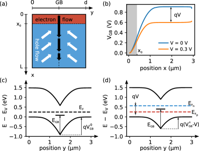
Because holes are majority carriers in the bulk of the absorber, the hole quasi-Fermi level is flat and equal to . We derived in Appendix B a criterion under which the hole quasi-Fermi level is flat across the grain boundary, so that the bulk quasi-Fermi level extends to the grain boundary core. Using Eq. (18) and the assumption of flat hole quasi-Fermi level, the distance between and the valence band is . The hole density at the grain boundary therefore reads
| (19) |
The hole density is shown in Fig. 2(b) (blue continuous lines). The electron density is equal to its equilibrium value Eq. (9) for , shown in Fig. 2(a). Because is much larger than all the other terms in the denominator of Eq. (17), the recombination simplifies to
| (20) |
for . The recombination is uniform for and negligible in the -region, so the dark recombination current reads
| (21) |
The features of Eq. (21) are a saturation current , an ideality factor of 1, and an activation energy .
In Appendix B we derive a condition under which the hole quasi-Fermi level is approximately flat. This condition reads ()
| (22) |
For , , , , Eq. (22) is satisfied for . Over the course of this work, we found this numerical value to be an acceptable threshold for all the grain boundary regimes of this section.
IV.2 Grain boundary recombination for
We turn to , also called “-type” regime. In this case the distance between and does not change with the applied voltage , as seen in Figs. 4(c) and (d). We further assume that is flat equal to ††footnotemark: . As a result Eq. (15) shows that the grain boundary built-in potential is independent of the applied voltage for . This is shown in Fig. 4(b).
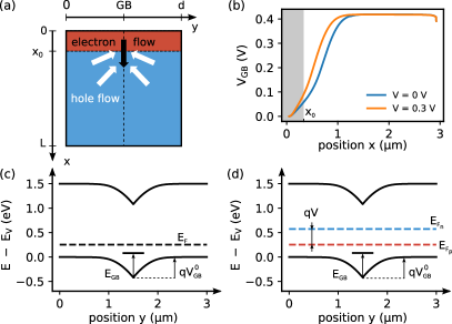
The electron transport is more complex than in the previous case. In particular, the electron quasi-Fermi level is not always equal to along the grain boundary, but varies significantly to accommodate the electron current. The grain boundary built-in potential confines electrons near the grain boundary core, leading to a one-dimensional motion along it. As a result, the continuity equation around the grain boundary reduces to a one-dimensional equation along the grain boundary core (-direction). Upon solving this equation beyond (see Appendix C), the electron density reads
| (23) |
where (: electron diffusion coefficient) is the diffusion length of electrons along the grain boundary. is the length scale of the confinement of the electrons to the grain boundary core. This length is related to , the electric field transverse to the grain boundary in the neutral region of the junction, by (see Eq. (70) in Appendix C). The electron density described here is shown in Fig. 2(a) (dashed orange line). The hole density (shown in Fig. 2(b)) is equal to its equilibrium value Eq. (10). Because dominates the denominator of Eq. (17), the recombination reads
| (24) |
for . We now consider two limiting cases for the integration of the recombination.
The first limit is the large diffusion length, , obtained for large mobilities and small values of recombination velocity. The electron density is uniform for , leading to the dark recombination current
| (25) |
In the second limit, , the electron mobility is small so that the electron density decays rapidly beyond . The recombination is peaked on both sides of and the recombination current reads
| (26) |
The description of this regime is shown in Fig. 4(a). Holes converge to where they recombine, generating a localized electron current. Both regimes have similar features: the saturation current varies as , the ideality factor is 1 and the thermal activation energy is .
IV.3 Grain boundary recombination for
As we increase the applied voltage in either of the previous cases, and become negligible compared to and respectively. Because the system approximately maintains the level occupancy close to its thermal equilibrium value, the carrier densities satisfy the relation
| (27) |
Equation (27) leads to , defining the “high-recombination” regime.
While the electrostatic potential now varies along the grain boundary, the built-in potential still confines the electrons to one-dimensional motion along the grain boundary core. Similarly to the regime , a one-dimensional continuity equation describes the electron transport along the grain boundary. Upon solving this equation (see Appendix D), we find the carrier densities
| (28) | ||||
| (29) |
where ( is the characteristic length of the electric field across the grain boundary). These densities yield the grain boundary recombination
| (30) |
for . We consider two limiting cases for the recombination current.
Because of the factor in , common material parameters for CdTe lead to large diffusion lengths such that . The uniform grain boundary (for ) described in Sec. IV.1 applies in this case, and the recombination current reads
| (31) |
For smaller values of the electron diffusion length, and the recombination is peaked at with the electron and hole flows depicted in Fig. 4(a). The dark recombination current therefore reads
| (32) |
In both limits the thermal activation energy is and the ideality factor is 1. Note that the factor is on the order of to for typical doping densities. As a result, is effectively reduced by two orders of magnitude, significantly reducing the amplitude of the grain boundary recombination current.
For equal , this difference between the single donor case and the single acceptor+donor state studied in Ref. Gaury and Haney, 2016 comes from the difference in band bending associated with the two cases. For the donor case, the band bending is substantially increased (see Eq. (15)) relatively to the donor+acceptor case. The increased band bending leads to suppressed hole density, which in turn suppresses electron-hole recombination.
IV.4 Numerical verification of the analytical results
We verify the accuracy of our analytical results using numerical solutions of the drift-diffusion-Poisson equations. We used our own finite-difference software to solve these equations for our geometry in Fig. 1(a). We discretized the electron/hole currents using the Scharfetter-Gummel scheme Gummel (1964), and used the Newton-Raphson method to find the self-consistent solution. To determine the electrostatic potential boundary conditions, we performed two steps. First, we solved the thermal equilibrium Poisson equation with at each contact. Then, we solved the full drift-diffusion-Poisson equations by imposing and , where is the equilibrium potential. Table 2 gives the list of material parameters used for these calculations.
| Param. | Value | Param. | Value |
|---|---|---|---|
Figure 5 presents calculations for the grain boundary dark current. At each applied voltage the current is given by the smallest value between the -type, -type and high recombination regimes.
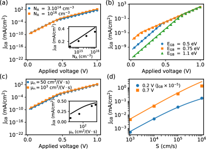
The doping density is varied in Fig. 5(a) for . The crossover from the -type regime () to the high recombination regime () occurs at about , as seen from the slope change. The inset shows the doping dependence of the high recombination regime. Contrary to the case studied in Ref. Gaury and Haney, 2016 where common material parameters for CdTe lead to decreasing grain boundary dark currents with doping at high voltages, the donor state shows the opposite behavior. The key difference between these cases lies in the effective electron surface recombination velocity entering the definition of the electron diffusion length at high voltages. In the single acceptor+donor case it is given by , while in the single donor case we found . Because the latter value is orders of magnitude smaller than the former. The primary consequence is that for the same , the diffusion length is much larger in the donor case. In turn, the limit is the relevant one for common CdTe parameters with the single donor state (Eq. (31)), while the opposite limit is relevant for the case studied in Ref. Gaury and Haney, 2016. An increasing doping density increases the depletion charge, leading to a larger value of . Consequently the factor in Eq. (31) is responsible for the increase in recombination current with doping density observed here. This increase is a major difference that will reflect in the open-circuit voltage.
We show the various grain boundary types in Fig. 5(b), where and correspond respectively to a -type and -type grain boundary at equilibrium. Figure 5(c) shows the dependence of the grain boundary dark current with electron mobility. This dependence is absent at low voltage, as shown by the limiting case Eq. (25). At higher voltages, the relevant limit is Eq. (31), as discussed above, which is independent of mobility. This limit explains the weak mobility dependence shown in the inset. Finally, Fig. 5(d) shows the scalings of the grain boundary dark current with surface recombination velocity. We show grain boundary dark currents in the -type regime (dots) and high-recombination regime (squares). On this plot both scalings are equal. The dark current scales as at low voltage, and as at high voltage. The second scaling is given by Eq. (31) which is the relevant limit in this case. With these scalings are identical.
V Grain boundary dark recombination current of a continuum of defect states
We turn to the case of a continuum of donor and acceptor states in the absorber band gap. We assume densities of states uniform in energy: , , where
| (33) |
determines the ratio of acceptor to donor densities of states. More acceptor (donor) states leads to -type (-type) grain boundary core. The neutral energy level of the distribution of gap states is (see Sec. II).
Under nonequilibrium conditions the grain boundary dark current is given by Eq. (16) where the integral along the grain boundary (-direction) now starts from . The recombination is the sum of the contributions from the acceptor and donor states (represented by the superscript )
| (34) |
Despite the apparent complexity of a continuum of states as opposed to a single state, the physical description of the nonequilibrium electron and hole currents is the same as given in Ref. Gaury and Haney, 2016. This apparent complexity will be incorporated in effective surface recombination velocities in what follows. The results of Ref. Gaury and Haney, 2016 and of this section are gathered in the last two rows of Table 1.
V.1 Grain boundary recombination for
We begin with the regime (-type grain boundary). In this regime the electron quasi-Fermi level is pinned to . The recombination is determined by holes, which flow from the -type grain interior into the grain boundary core. Because most of the absorber is -type, the recombination is uniform along the entire grain boundary. We refer to Sec. III A of Ref. Gaury and Haney, 2016 for a more complete description of this regime.
The electron density is independent of voltage and spatially uniform, given by Eq. (9) with . The hole density is also uniform and reads
| (35) |
The grain boundary dark current reads
| (36) |
where is the effective surface recombination velocity
| (37) |
The integrals in Eq. (37) can be computed analytically but the results are cumbersome and difficult to interpret. To give a sense of these integrals, we refer to the solid blue line of Fig. 6(b) where we show the grain boundary recombination as a function of energy. This figure shows that only states with energies contribute significantly to the recombination. The upper limit results from the fact that states above are empty of electrons. The lower limit is the energy at which holes are emitted from the defect state to the valence band faster than electrons relax from the conduction band to the defect state. This rapid hole emission rate prevents recombination. The typical width of the integrand of is
| (38) |
as shown on the continuous plot of Fig. 6(b). Equation (37) therefore simplifies to
| (39) |
Note that the occupancy of the gap states is independent of the applied voltage in this regime (see the continuous curve in Fig. 6(a)). That is because the occupancy of the gap states is determined solely by the electron density, which is independent of voltage here.
In Appendix B we derive a condition under which the hole quasi-Fermi level is approximately flat. This condition applied here reads ()
| (40) |
For , , , , , Eq. (40) is satisfied for . This value is in the range of standard bulk mobilities for CdTe Sellin et al. (2005); Duenow et al. (2014). We found this order of magnitude to be an acceptable threshold for all the grain boundary regimes with the continuum of defect states.
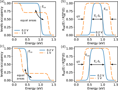
V.2 Grain boundary recombination for
In the regime (-type grain boundary), the hole quasi-Fermi level is pinned to . In this regime the recombination is determined by electrons flowing into the grain boundary core from regions of the grain interior where . These regions correspond to in Fig. 1(a). The recombination is therefore mainly concentrated within the - region of the junction depletion region, and is uniform for . We refer to Sec. III B of Ref. Gaury and Haney, 2016 for a complete description of this case.
For , the hole density is uniform given by Eq. (10) with ; the electrons are confined to the grain boundary core by the grain boundary built-in electric field, leading to a one-dimensional diffusion along it. Solving the one-dimensional diffusion equation leads to the electron density
| (41) |
where (: electron diffusion coefficient) is the electron diffusion length, and is the length scale of the confinement (: electric field transverse to the grain boundary in the bulk of the junction). is the effective surface recombination velocity in this case
| (42) |
The grain boundary dark current reads
| (43) |
The integrals in have a similar interpretation as for the -type grain boundary: only the states with energies contribute significantly to the recombination, as shown in Fig. 6(d). The lower limit results from the fact that states below are empty of holes. The upper limit is the energy at which electrons are emitted from the defect state to the conduction band faster than holes relax from the valence band to the defect state. The integrands in exhibit the same shape as . In particular, the width of the integrand is still given by Eq. (38). Equation (42) therefore simplifies to
| (44) |
Similarly to the -type grain boundary, the occupancy of the gap states is determined solely by holes and is therefore independent of the applied voltage, shown in Fig. 6(c).
V.3 Grain boundary recombination for
As the applied voltage is increased above , the minority carrier density approaches the majority carrier density at the grain boundary. This results in a rearrangement of the gap states occupancies. However, we use the assumption that the grain boundary charge does not change with voltage, as discussed in Sec. III, which leads to the constraint
| (45) |
The change in occupancies keeps the area under the occupancy curves equal to its equilibrium value, as shown by the dashed lines in Figs. 6(a) and (c). More specifically, occupancies above increase while the ones below decrease. These changes lead to an increase of the number of states contributing to the recombination as can be seen in Figs. 6(b) and (d).
There is no pinning of either quasi-Fermi level to in this regime. We refer to Sec. III C of Ref. Gaury and Haney, 2016 for the derivations in this case. We can show that the constraint Eq. (45) imposes that the ratio of carrier densities remains constant along the grain boundary. While this ratio was independent of voltage for the single acceptor+donor state of Ref. Gaury and Haney, 2016, this is not the case anymore. Assuming , and solving a one-dimensional diffusion equation along the grain boundary leads to the carrier densities
| (46) | ||||
| (47) |
We find by solving Eq. (45). This ratio gives the value of the plateau reached by the levels occupancy at energies around midgap, as shown by the dashed lines in Figs. 6(a) and (c). Because and dominate the level occupancy Eq. (2) at these energies, the value of the plateau is , with . Considering (unrealistically) large values of applied voltage such that the levels occupancy is entirely independent of energy, we find that converges to
| (48) |
In Eqs. (46) and (47), is the diffusion length of electrons along the grain boundary, and is the characteristic length of the electric field transverse to the grain boundary. The effective surface recombination velocity reads
| (49) |
The integrand of Eq. (49) now varies with voltage as shown by the dashed line in Fig. 6(b). It can be shown that an approximation for the integral is
| (50) |
Gathering the above results leads to the grain boundary dark current
| (51) |
This result is formally similar to the corresponding case for the single acceptor+donor state studied in Ref. Gaury and Haney, 2016, yet the voltage dependence of the effective surface recombination velocity is a key difference. Taking , Eq. (51) is proportional to . This shows that when the distribution of gap states is skewed towards either donors or acceptors (e.g. big or small ), the recombination current is diminished. This reduction can be understood with the levels occupancy in Fig. 6(c) (dashed line). The recombination plotted in Fig. 6(d) shows that the states around midgap contribute the most to the recombination. These states correspond to the plateau of the levels occupancy, which is approximately equal to here. For large or small , the plateau is far from , which reduces the probability that a hole and an electron be captured together by a gap state. This reduced probability leads to a reduction of the recombination current.
In all three gap state configurations studied (single and continuum of acceptor+donor, single donor), the high recombination regime exhibits a thermal activation energy and an ideality factor of 2 (both typical of recombination determined by electrons and holes equally). These characteristics were observed in previous experimental work on Si junctions aiming to isolate the grain boundary recombination current Neugroschel and Mazer (1982).
V.4 Numerical verification of the analytical results
The numerical tests to verify the accuracy of the results of this section are presented in Fig. 7. These results were obtained with . For applied voltages below , the current is given by the smallest value between the -type and -type regimes. For higher values of applied voltage we used the high recombination regime. For all plots except Fig. 7(b) we used , which leads to (-type grain boundary).
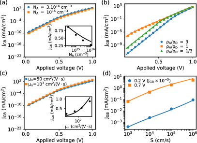
We vary the doping density in Fig. 7(a). Before the change of slope, the dark current is given by Eq. (43) which exhibits a doping dependence mostly via the width of the -region . The reduction of the slope reveals the crossover to the high recombination regime () where the dark current is given by Eq. (51). In this regime, the inset shows the predicted scaling in .
Fig. 7(b) shows the grain boundary dark current for various ratios . In descending order, these correspond to grain boundary neutral levels , and . The crossover to the high recombination regime occurs when the occupancy of the gap states starts to change significantly, that is for (see Fig. 6(b) and (d)).
The dependence of the dark current with electron mobility is shown in Fig. 7(c). At low voltage, this dependence is barely visible but present. The dependence is weak in the -type regime because both limiting cases of Eq. (43), and , are independent of mobility. The chosen set of parameters lies in between these limits. At high voltages we verify the square root scaling as shown by Eq. (51) in the limit . Increasing electron mobility reduces the suppression of carrier den- sities away from the maximum of recombination by increasing the electron diffusion length . The increase of , in turn, increases the recombination along the grain boundary.
Fig. 7(d) shows the scalings of the grain boundary dark current with surface recombination velocity . Because we used equal surface recombination velocities for the donor and acceptor states, and electrons and holes, the effective recombination velocities and are proportional. The notable feature of this plot is the scaling of the grain boundary recombination current obtained at high voltage. This feature only appears at high recombination velocities as it requires , as shown by Eq. (51). In the opposite limit one recovers a linear scaling in .
VI Open-circuit voltage
We now consider a charged grain boundary under illumination and derive relations for the open-circuit voltage . We assume that around the current-voltage relation under illumination is given by the sum of the short circuit current and the dark current (see Sec. V of Ref. Gaury and Haney, 2016 for a discussion on the validity of this assumption). The dark current is the sum of the grain boundary dark current (derived in Sec. III and Sec. IV) and the bulk recombination current. We use the results of Sec. IV of Ref. Gaury and Haney, 2016 for the bulk recombination whenever necessary.
Neglecting the bulk recombination and the non-exponential voltage dependences in the grain boundary dark currents, we can write down explicit forms for the open-circuit voltage associated with the grain boundary recombination. The general form of the open-circuit voltage reads
| (52) |
where is a surface recombination velocity, is a length characteristic of the physical regime, is an effective density of states, is an activation energy, is the applied voltage and is an ideality factor. Even though Eq. (52) is not mathematically correct in all cases (because it neglects non-exponential voltage dependence), it captures the dominant scalings for the physical parameters and should give the reader an intuition for how these parameters impact . The parameters entering Eq. (52) are shown in Table 1 for all grain boundary configurations.
VI.1 Single donor state
We begin with the single donor state in the gap of the absorber material. The parameters in Eq. (52) for this case are given in the first row of Table 1. Fig. 8 shows comparisons between the numerically computed , and the values obtained with the numerically computed and the analytic forms of the dark current.
These results differ somewhat from the single donor+acceptor defect case of Ref. Gaury and Haney, 2016. As we discussed in Sec. IV.4, the single donor state with common material parameters for CdTe exhibits increasing grain boundary dark currents with doping at high voltages. As a result, decreases with doping as shown in Fig. 8(a). Figure 8(b) shows that the open-circuit voltage as a function of defect energy level is not symmetrical from midgap. In fact, for the open-circuit voltage is given by the grain boundary recombination current of the -type regime Eq. (21), while for lower values, the open-circuit voltage is given by the regime and Eq. (31) (high recombination regime). The plot shows that donor states close to the band edge (i.e. -type grain boundaries) are more favorable to . These states are less easily accessible to holes than over states, hence reducing the probability for recombination. Figure 5(b) shows that, for a given applied voltage, the amplitude of the grain boundary recombination current of the -type regime is smaller than the one of the high recombination regime (hence the larger in the first case). Figure 8(c) shows the dependence with electron mobility for values higher than . Under the chosen conditions the grain boundary recombination current depends weakly on mobility. Finally the logarithmic dependence on surface recombination velocity of Eq. (52) is shown in Fig. 8(d).
A key difference between this single donor case and the donor+acceptor case of Ref. Gaury and Haney, 2016 is the amplitude of the grain boundary recombination in the high recombination regime. In the single donor state of the present work, the electron surface recombination velocity is effectively reduced by the factor (which can be on the order of in the regime of large defect density of states) as can be seen in the expressions of the carrier densities Eqs. (28) and (29), as well as in the recombination itself Eq. (30). As a result, for intermediate values of bulk lifetime (), the bulk recombination current is of the same order of magnitude as the
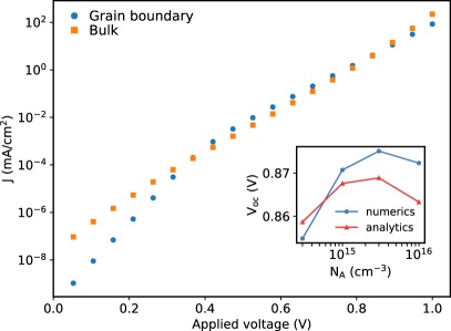
grain boundary recombination current with , as shown in Fig. 9. In this example, reducing the doping density increases the bulk recombination (because the width of the junction depletion region increases) which now dominates over the grain boundary contribution. The inset of Fig. 9 shows that the resulting open-circuit voltage increases with doping, contrary to the behavior shown in Fig. 8(a) for which .
VI.2 Continuum of gap states
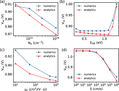
We now turn to the continuum of acceptor and donor states. The parameters in Eq. (52) are given in the last row of Table 1. Note that in the high recombination regime (), Eq. (52) applies when neglecting the linear voltage dependence of the effective surface recombination velocity (see Eq. (50)). Despite this approximation, Eq. (52) provides the correct overall scalings with doping density, distribution of states, mobility and surface recombination velocities. Fig. 10 shows the comparisons of the simulated open-circuit voltages with our analytical results.
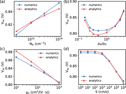
The continuum of states studied here has lots of features similar to the single acceptor+donor state studied in Ref. Gaury and Haney, 2016. In particular we find the same scalings of with doping, mobility and surface recombination velocity shown in Fig. 10(a), (c) and (d). A difference with Ref. Gaury and Haney, 2016 is the U-shape dependence of with the ratio , presented in Fig. 10(b). The open-circuit voltage now varies with (i.e. with the effective single state value) even for intermediate values of the ratio. This is because the grain boundary recombination current in the high recombination regime depends on this ratio via as shown by Eq. (48).
Figure 10(b) shows that gap state configurations with ratios away from 1 give better values. Note that we have assumed equal values of short circuit current for all values of grain boundary parameters. This will certainly not be the case in practice. Indeed, for grain boundaries which do not undergo type inversion (e.g. -type grain boundaries), we find that the short circuit current density is decreased. Therefore, only gap state configurations with more donor states will be beneficial for photovoltaic performance for the model configurations studied in this paper.
VII Conclusion
We generalized the physical descriptions associated with the microscopic charge transport and recombination of Ref. Gaury and Haney, 2016 to two additional configurations of gap states: a single donor state and a continuum of donor and acceptor states. In this work we derived the corresponding analytic expressions for the grain boundary dark recombination current. We found that all these configurations share three similar regimes describing the grain boundary dark recombination current as a function of voltage (-type, -type and high-recombination). However, they exhibit differences in the amplitude of the subsequent recombinations. Mixtures of acceptor and donor states (single level and continuum) result in enhanced recombination that reduces the open-circuit voltage for a wide range of bulk lifetimes. The amplitudes of recombination for the single donor state are lower, and commensurate with the bulk recombination for intermediate bulk lifetimes. From this work and Ref. Gaury and Haney, 2016, we observed that a larger concentration of donor states compared to acceptor states improve the device open-circuit voltage for a fixed value of the short circuit current density.
Nanoscale imaging and spectroscopy combined with first principles calculations can now determine, at least in principle, the electronic configuration of grain boundaries Yan et al. (2015). In turn, this knowledge can be used within the framework developed here to obtain quantitative predictions of device open-circuit voltage. In this way, our work provides a bridge between nanoscale characterization and macroscopic device response. Finally, our approach and the physical descriptions of grain boundaries presented here extend beyond CdTe or Cu(In,Ga)Se2 technologies. For example, our approach could be applied to grain boundaries with upward band banding resulting from negatively charged boundaries in -type materials or alternatively, positively charged boundaries in -type materials.
Acknowledgements.
B. G. acknowledges support under the Cooperative Research Agreement between the University of Maryland and the National Institute of Standards and Technology Center for Nanoscale Science and Technology, Award 70NANB14H209, through the University of Maryland.Appendix A Conditions for large defect density regime
We derive the minimal defect densities for which for the single donor defect state and the continuum of defect states. Because the defect statistics in thermal equilibrium are different in each case (see Eq. (5) and Eq. (6) respectively), we must derive two different criteria.
We start with the single donor state. The condition requires that . We specify this requirement by imposing that the Fermi level lies at least above the defect level at the grain boundary,
| (53) |
This condition together with Eq. (11) imposes
| (54) |
where . Using a depletion approximation and , the charge in the depleted regions surrounding the grain boundary is
| (55) |
Equating Eq. (5) and Eq. (55) leads to the critical defect density of states
| (56) |
For the case of the continuum of acceptor and donor states, the large defect density of states corresponds to the pinning of the Fermi level to the neutral point of the gap states distribution. We will consider the large defect density regime when the distance between and is smaller than . Using a depletion approximation and , the charge in the depleted regions around the grain boundary is
| (57) |
Equating Eqs. (1) and (57) leads to the critical value
| (58) |
where with . This critical donor density of states depends on the ratio considered. Also note that because the denominator of Eq. (58) depends on energy, is a density of states per energy unit (expressed in ).
Appendix B Condition for nearly flat hole quasi-Fermi level
We specify the domain of validity of the assumption of flat hole quasi-Fermi level. In the main text we consider when variations of across the grain boundary are smaller than . An expansion of across the grain boundary yields
| (59) |
where the gradient of at the grain boundary depends on the regime considered (e.g. -type grain boundary). The single donor state and the continuum of defect states require formally the same condition. The relevant surface recombination velocity must be used in each case. We are able to derive such a criterion only for an -type grain boundary but found that it applies well also in other regimes. In what follows we focus on the single donor state.
In the regime , the gradient of is obtained by integrating the continuity equation for holes across the grain boundary over an infinitely small distance,
| (60) |
Assuming that the variation of across the grain boundary follows that of the electrostatic potential, the distance across the grain boundary where is given by a depletion approximation . The assumption of flat is therefore valid for
| (61) |
For the continuum of states one would use instead.
Appendix C Derivations for -type donor defect state
Using the energy scale and definitions of Fig. 4(d), the carrier densities at the grain boundary are given by
| (62) | ||||
| (63) |
where is the electrostatic potential at the grain boundary. The zero of electrostatic potential is at the -contact away from the grain boundary. In the -type donor state, the electrostatic potential is uniform along the grain boundary in the bulk of the junction and is independent of voltage. The value of is determined by the grain boundary built-in potential at thermal equilibrium,
| (64) |
where is given by Eq. (15). The grain boundary recombination is maximum at , where is the point where the carrier densities in the grain interior are equal. We consider that the grain interior recombination is peaked at the same point. Using a depletion approximation in the depletion region of the junction in the grain interior, we find that at
| (65) |
where is the junction built-in potential (the dependence of on applied voltage is weak and can be neglected). Using the potential Eq. (64) in Eqs. (62) and (63), and assuming that (see justification above Eq. (19)), we obtain expressions for the carrier densities beyond ,
| (66) | ||||
| (67) |
Despite the above formulation, these relations are valid only for . We extend their domain of validity to for the purpose of calculating the recombination, where the errors we make here on and cancel out.
For we use the continuity equation for electrons to obtain ,
| (68) |
where is the bulk recombination and the electron current component along the grain boundary is given by
| (69) |
In the above equation we assumed that the electron density across the grain boundary decays as , where
| (70) |
is the characteristic length associated with the electric field transverse to the grain boundary in the bulk region. This exponential decay assumes that is flat around the grain boundary, which coincides with the fact that the currents going to the grain boundary are small. Integrating Eq. (68) in the -direction around the grain boundary leads to
| (71) |
where we neglected the currents in the -direction at the end of the grain boundary depletion region, and the bulk recombination. We introduce the effective diffusion length , where is the electron diffusion constant, to rewrite Eq. (71) as
| (72) |
Considering that at , and neglecting the diverging part of the solution of Eq. (72), we obtain
| (73) |
We verify the accuracy of Eq. (73) in Fig. 11(b) (black dashed curve).
Inserting Eq. (73) into Eq. (66) yields the electron density given in the main text
| (74) |
Because , the recombination at the grain boundary reads
| (75) |
We integrate over the length of the grain boundary to obtain the recombination current
| (76) |
Equation (76) is the general result in the case .
Appendix D Derivations for donor state in the high recombination regime
Here we provide the derivations of the analytical results presented in Sec. IV.3. In the high recombination regime there is a constant such that along the grain boundary. In addition , so that we get
| (77) |
Similarly to the -type case, the recombination is peaked at and decays after that point so we focus the derivation beyond .
From here on the derivation of follows the exact same steps as Appendix C starting with the continuity equation:
| (78) |
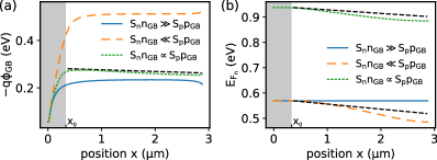
where . is the characteristic length associated with the electric field transverse to the grain boundary. is again the bulk recombination. Because the grain boundary built-in potential is not uniform in this regime, the transverse electric field depends on the location along the grain boundary. While does not correspond to a precise field, we find that it accurately determines the slopes of the electron quasi-Fermi level and the electrostatic potential along the grain boundary. The electron current is still given by Eq. (69) with the change of for . Integrating Eq. (78) around the grain boundary leads to
| (79) |
where we neglected the currents in the -direction at the end of the grain boundary depletion region, and the bulk recombination. We introduce the effective diffusion length , and assume that [30] to rewrite Eq. (79) as
| (80) |
Considering that at we obtain
| (81) |
Since , we can equate Eqs. (62) and (63) to get
| (82) |
which yields the electrostatic potential along the grain boundary
| (83) |
Comparisons of Eq. (81) and Eq. (83) with numerical data are shown in Figs. 11(a) and 11(b) respectively (dotted green curves). We see that the numerically computed potential and electron quasi-Fermi level are not linear over the entire length of the grain boundary, however the analytical results give a good approximation of the slopes near the depletion region.
Inserting Eqs. (81) and (83) into the densities Eqs. (62) and (63) yields the densities given in Sec. IV.3. These densities yield the grain boundary recombination
| (84) |
Integrating the recombination over the length of the grain boundary gives the recombination current
| (85) |
Equation (85) is the general result in the case .
The constant can be specified considering that the occupancy of the grain boundary defect level remains equal to its thermal equilibrium value . We thus find
| (86) |
assuming that because of the high defect density of states.
References
- Green et al. (2017) M. A. Green, K. Emery, Y. Hishikawa, W. Warta, E. D. Dunlop, D. H. Levi, and A. W. Y. Ho-Baillie, “Solar cell efficiency tables (version 49),” Prog. Photovolt. Res. Appl. 25, 3–13 (2017).
- Geisthardt et al. (2015) R. M. Geisthardt, M. Topič, and J. R. Sites, “Status and potential of cdte solar-cell efficiency,” IEEE J. Photovolt. 5, 1217–1221 (2015).
- Jiang et al. (2004) C.-S Jiang, R. Noufi, K. Ramanathan, J. A. AbuShama, H. R. Moutinho, and M. M. Al-Jassim, “Does the local built-in potential on grain boundaries of thin films benefit photovoltaic performance of the device?” Applied Physics Letters 85, 2625–2627 (2004).
- Visoly-Fisher et al. (2006) I. Visoly-Fisher, S. R. Cohen, K. Gartsman, A. Ruzin, and D. Cahen, “Understanding the beneficial role of grain boundaries in polycrystalline solar cells from single-grain-boundary scanning probe microscopy,” Adv. Funct. Mater. 16, 649–660 (2006).
- Gloeckler et al. (2005) M. Gloeckler, J. R. Sites, and W. K. Metzger, “Grain-boundary recombination in solar cells,” J. Appl. Phys. 98, 113704 (2005).
- Taretto and Rau (2008) K Taretto and U Rau, “Numerical simulation of carrier collection and recombination at grain boundaries in solar cells,” J. Appl. Phys. 103, 094523 (2008).
- Rau et al. (2009) U. Rau, K. Taretto, and S. Siebentritt, “Grain boundaries in thin-film solar cells,” Appl. Phys. A 96, 221–234 (2009).
- Troni et al. (2013) F. Troni, R. Menozzi, E. Colegrove, and C. Buurma, “Simulation of current transport in polycrystalline CdTe solar cells,” J. Electron. Mater. 42, 3175–3180 (2013).
- Zhao et al. (2016) Y. Zhao, M. Boccard, S. Liu, J. Becker, X.-H. Zhao, C. M. Campbell, E. Suarez, M. B. Lassise, Z. Holman, and Y.-H. Zhang, “Monocrystalline CdTe solar cells with open-circuit voltage over V and efficiency of ,” Nat. Energy 1, 16067 (2016).
- Burst et al. (2016) J. M. Burst, J. N. Duenow, D. S. Albin, E. Colegrove, M. O. Reese, J. A. Aguiar, C.-S. Jiang, M. K. Patel, M. M. Al-Jassim, D. Kuciauskas, S. Swain, T. Ablekim, K. G. Lynn, and W. K. Metzger, “CdTe solar cells with open-circuit voltage breaking the V barrier,” Nat. Energy 1, 16015 (2016).
- Kanevce et al. (2017) A. Kanevce, M. O. Reese, T. M. Barnes, S. A. Jensen, and W. K. Metzger, “The roles of carrier concentration and interface, bulk, and grain-boundary recombination for 25% efficient CdTe solar cells,” J. Appl. Phys. 121, 214506 (2017).
- Gaury and Haney (2016) B. Gaury and P. M. Haney, “Charged grain boundaries reduce the open-circuit voltage of polycrystalline solar cells–An analytical description,” J. Appl. Phys. 120, 234503 (2016).
- Edmiston et al. (1996) S. A. Edmiston, G. Heiser, A. B. Sproul, and M. A. Green, “Improved modeling of grain boundary recombination in bulk and p-n junction regions of polycrystalline silicon solar cells,” J. Appl. Phys. 80, 6783–6795 (1996).
- Rudmann et al. (2004) D. Rudmann, A. F. Da Cunha, M. Kaelin, F. Kurdesau, H. Zogg, A. N. Tiwari, and G. Bilger, “Efficiency enhancement of solar cells due to post-deposition Na incorporation,” Appl. Phys. Lett. 84, 1129–1131 (2004).
- Kumar and Rao (2014) S. G. Kumar and K.S.R. K. Rao, “Physics and chemistry of CdTe/CdS thin film heterojunction photovoltaic devices: fundamental and critical aspects,” Energy Environ. Sci. 7, 45–102 (2014).
- Yoon et al. (2013) H. P. Yoon, P. M. Haney, D. Ruzmetov, H. Xu, M. S. Leite, B. H. Hamadani, A. A. Talin, and N. B. Zhitenev, “Local electrical characterization of cadmium telluride solar cells using low-energy electron beam,” Sol. Energ. Mat. Sol. Cells 117, 499–504 (2013).
- Moutinho et al. (2010) H. R. Moutinho, R. G. Dhere, C.-S. Jiang, Y. Yan, D. S. Albin, and M. M. Al-Jassim, “Investigation of potential and electric field profiles in cross sections of CdTe/CdS solar cells using scanning kelvin probe microscopy,” J. Appl. Phys. 108, 074503 (2010).
- Tuteja et al. (2016a) M. Tuteja, P. Koirala, V. Palekis, S. MacLaren, Chris S. Ferekides, R. W. Collins, and A. A. Rockett, “Direct observation of treatment induced grain boundary carrier depletion in cdte solar cells using scanning probe microwave reflectivity based capacitance measurements,” J. Phys. Chem. C 120, 7020–7024 (2016a).
- Sellin et al. (2005) P. J. Sellin, A. W. Davies, A. Lohstroh, M. E. Ozsan, and J. Parkin, “Drift mobility and mobility-lifetime products in CdTe:Cl grown by the travelling heater method,” IEEE Trans. Nucl. Sci. 52, 3074–3078 (2005).
- Duenow et al. (2014) J. N. Duenow, J. M. Burst, D. S. Albin, D. Kuciauskas, S. W. Johnston, R. C. Reedy, and W. K. Metzger, “Single crystal CdTe solar cells with greater than 900 mV,” Appl. Phys. Lett. 105, 053903 (2014).
- Shockley and Read (1952) W. Shockley and W. T. Read, “Statistics of the recombinations of holes and electrons,” Phys. Rev. 87, 835–842 (1952).
- Johnson et al. (2005) P. K. Johnson, J. T. Heath, J. D. Cohen, K. Ramanathan, and J. R. Sites, “A comparative study of defect states in evaporated and selenized CIGS(S) solar cells,” Prog. Photovolt: Res. Appl. 13, 579–586 (2005).
- Krasikov and Sankin (2017) D. Krasikov and I. Sankin, “Defect interactions and the role of complexes in the CdTe solar cell absorber,” J. Mater. Chem. A 5, 3503–3513 (2017).
- Rohderick (1978) E. H. Rohderick, Metal-semiconductor contacts (Oxford Univ. Press, 1978).
- Note (1) We will restrict to the interval .
- Note (2) The general net capture rate for electrons at the grain boundary core is . At thermal equilibrium this rate is zero which gives Eq. (9). The same reasoning applies for holes and leads to Eq. (10).
- Tuteja et al. (2016b) M. Tuteja, A. B. Mei, V. Palekis, A. Hall, S. MacLaren, C. S. Ferekides, and A. A. Rockett, “ treatment-induced enhanced conductivity in CdTe solar cells observed using conductive atomic force microscopy,” J. Phys. Chem. Lett. 7, 4962–4967 (2016b).
- Moseley et al. (2015) J. Moseley, W. K. Metzger, Helio R. Moutinho, N. Paudel, H. L. Guthrey, Y. Yan, R. K. Ahrenkiel, and M. M. Al-Jassim, “Recombination by grain-boundary type in CdTe,” J. Appl. Phys. 118, 025702 (2015).
- Gummel (1964) H. K. Gummel, “A self-consistent iterative scheme for one-dimensional steady state transistor calculations,” IEEE Transactions on electron devices 11, 455–465 (1964).
- Kuciauskas et al. (2015) D. Kuciauskas, A. Kanevce, P. Dippo, S. Seyedmohammadi, and R. Malik, “Minority-carrier lifetime and surface recombination velocity in single-crystal CdTe,” IEEE J. Photovolt. 5, 366–371 (2015).
- Suzuki et al. (2002) K. Suzuki, S. Seto, T. Sawada, and K. Imai, “Carrier transport properties of HPB CdZnTe and THM CdTe:Cl,” IEEE Trans. Nucl. Sci. 49, 1287–1291 (2002).
- Fink et al. (2006) J. Fink, H. Krüger, P. Lodomez, and N. Wermes, “Characterization of charge collection in CdTe and CZT using the transient current technique,” Nucl. Instr. Meth. Phys. Res. A 560, 435 – 443 (2006).
- Neugroschel and Mazer (1982) A. Neugroschel and J. A. Mazer, “Effects of grain boundaries on the current-voltage characteristics of polycrystalline silicon solar cells,” IEEE Trans. Electron Devices 29, 225–236 (1982).
- Yan et al. (2015) Y. Yan, W.-J. Yin, Y. Wu, T. Shi, N. R. Paudel, C. Li, J. Poplawsky, Z. Wang, J. Moseley, H. Guthrey, H. Moutinho, S. J. Pennycook, and M. M. Al-Jassim, “Physics of grain boundaries in polycrystalline photovoltaic semiconductors,” J. Appl. Phys. 117, 112807 (2015).