Metal-Insulator Transition in Ga doped ZnO via Controlled Thickness
Abstract
We report thickness dependent metal insulator transition in Ga doped ZnO (Ga:ZnO) thin films grown by pulsed laser deposition technique. From the electrical transport measurements, we find that while the thinnest film exhibits a resistivity of 0.05 -cm, lying in the insulating regime, the thickest has resistivity of -cm which shows metallic type of conduction. Our analysis reveals that the Mott’s variable range hopping (VRH) model governs the insulating behavior in the thinner Ga:ZnO whereas the 2D weak localization phenomena is appropriate to explain the electron transport in the thicker Ga:ZnO. Magnetoresistance study further confirms the presence of strong localization in 6 nm film while weak localization is observed in 20 nm and above thicker films. From the density functional calculations, it is found that due to surface reconstruction and Ga doping, strong crystalline disorder sets in very thin films to introduce localized states and thereby, restricts the donor electron mobility.
I Introduction
For last many decades, ZnO has remained a material of great research interest both in fundamental and applied aspects. Due to high excitonic binding energy (60 meV) and wide bandgap of 3.37 eV, ZnO has potential applications in optoelectronics devices like light emitting diodes (LED), photodetectors and laser diodesChu et al. (2008); Choi et al. (2010); Chu et al. (2011). In particular, this compound has been a subject of active investigation to exploit its potential as a transparent conducting oxide which can serve as an alternate to indium tin oxide (ITO)Minami (2000). The conductivity in n-type doped ZnO can be enhanced as high as 7000 S/cm through substitution of group III and IV elements at the Zn siteBhosle et al. (2006); Kuznetsov et al. (2015); Das et al. (2014). The large conductivity in this system is primarily attributed to the delocalized p-obitals carrying the donor electronsSans et al. (2009). Among these n-type dopants, Ga is the most suitable candidate to enhance the conductivity of ZnO since both Ga and Zn have almost similar ionic radii which helps in increasing the solubility of a dopant in the host material.
Recently, Look et al. has achieved a minimum resistivity of -cm with 3% Ga doping in ZnO thin films grown by pulsed laser deposition (PLD) techniqueLook et al. (2011). Earlier, Bhosle et al. had reported that 5% Ga doping yields minimum resistivity in ZnO thin films(Bhosle et al., 2006). It is observed that resistivity first decreases as doping concentration increases and after reaching a minimum value, it again increases since dopant itself starts acting as a scattering centerBhosle et al. (2006). Therefore, ZnO can exhibit metal insulator transition (MIT) by tuning the factors such as doping concentration. In fact, MIT in Ga doped ZnO as a function of doping concentration has been reported by several other groups Bhosle et al. (2006); Snure and Tiwari (2007). With sufficiently high doping concentration, the dopant electrons make ZnO degenerate as these electrons form a dispersive band. The MIT can also be achieved in degenerately doped ZnO by reducing the thickness. It has been experimentally observed that the conducting Si doped ZnO becomes highly resistive below a critical thickness of 15 nmDas et al. (2014). However, so far the thickness dependent MIT investigation is limited to Si doping only. Therefore, a detailed mechanism that causes the MIT has not been completely understood yet. In this work, we examine the possibility of MIT in Ga:ZnO, which shows maximum conductivity among all n-type dopants, as a function of film thickness.
To gain an in-depth understanding behind the thickness driven MIT, experimentally it is imperative to study the low temperature electrical properties of degenerately Ga:ZnO films as a function of thickness. Temperature dependent resistivity measurement undoubtedly reveals the metallic or insulating nature. For metallic sample temperature coefficient of resistance (TCR) is positive whereas for insulator TCR becomes negative. In addition, the occupancy and k-dispersion of the bands are good measures to examine the metallicity and thereby, the MIT. In this context, solutions to the quantum mechanical many body problems through ab initio calculations based on density-functional theory (DFT) are desirable.
In this paper, we present the structural, electrical and magnetotransport properties of Ga:ZnO thin films of varying thickness, in the range of 6 – 51 nm, grown on c-sapphire substrate. From the temperature dependent resistivity measurement, we observe MIT in Ga:ZnO films as a function of film thickness. For 6 nm thick film, the resistivity is found to be close to 0.05 -cm which lies in the insulating regime and conduction is governed by the variable range hopping (VRH) mechanism. For the film with thickness 20 nm and above, the resistivity is of the order of -cm. These films exhibit 2D weak localization phenomena at low temperature regime. Temperature dependent resistivity and magnetoresistance data confirm the presence of weak localization in films with thickness 20 nm and more while in 6 nm thick film exhibits strong localization behavior. Our density functional calculations suggest that, in thicker films, lattice distortion due to Ga dopant is weak and donor p-electron partially occupies a dispersive band in kx-ky plane which is the source of metallic type of conduction. However, in 6 nm film, surface reconstruction and the dopant induce sufficient lattice disorders which in turn create localized states in the vicinity of Fermi level and hence, the film exhibits insulating behavior.
II Experimental details
1% Ga doped ZnO (Ga:ZnO) thin films were deposited on (001) sapphire substrate (5 mm 5 mm) by PLD technique. A KrF laser of wavelength 248 nm of fluence 2 J/cm2 and 2 Hz pulse frequency was used for the deposition. The substrate to target distance was 4.5 cm. During the deposition, O2 partial pressure inside the chamber was maintained at mbar and the substrate temperature was 500 oC for all the samples. The number of laser pulses were varied to grow thin films of different thicknesses. A 4-circle high resolution XRD (HRXRD) (Rigaku Smartlab, Japan) was employed to investigate the structural quality and also to determine the thickness of the samples from X-ray reflectivity (XRR). These experiments were performed using a Ge (220) monochromator and the Cu K source. Temperature dependent electrical and magnetotransport measurements were carried out using a physical property measurement system (PPMS, Quantum Design) in the temperature range of 4 – 300 K.
III Experimental results
III.1 X-ray reflectivity
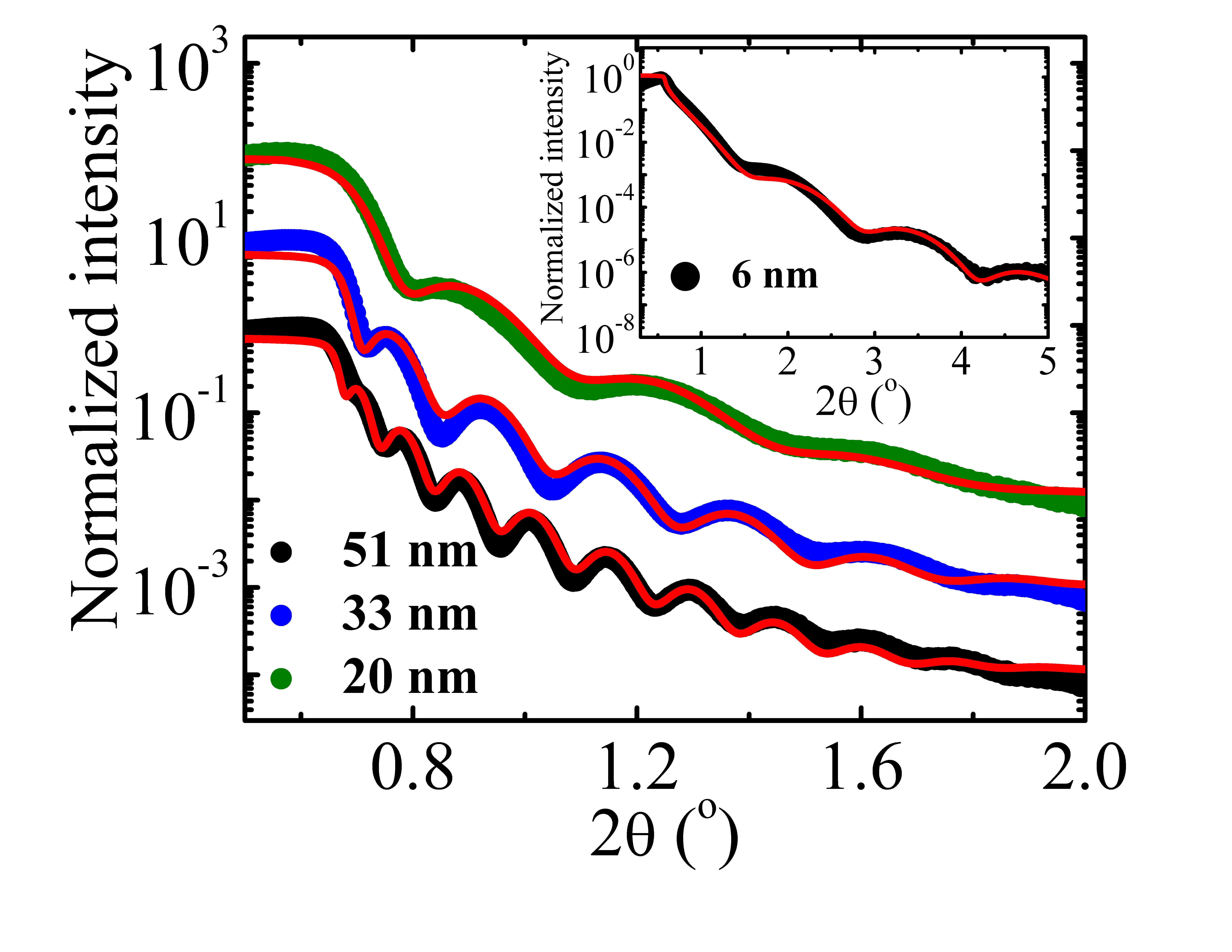
To precisely determine the film thickness, we have carried out X-ray reflectivity (XRR) on Ga:ZnO films. Figure 1 displays XRR profile of Ga:ZnO thin films of different thickness grown on c-sapphire substrate. XRR data was fitted using Globalfit software (Rigaku) to estimate the thickness and roughness of the films. It can be observed from the Fig. 1 that the fitted data are in excellent agreement with the experiment. The thickness values as obtained from the fit are indicated in the figure and have been used to analyze the electrical transport data. The root mean square (rms) roughness of the surface of each film lies below 0.7 nm implying an extremely smooth nature of Ga:ZnO films.
III.2 X-ray diffraction
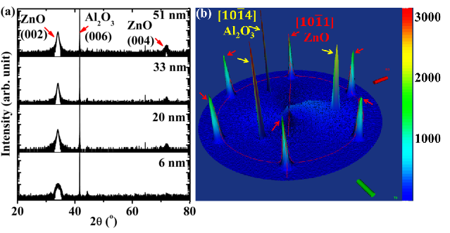
It is essential to check the crystallinity and the epitaxial nature of Ga:ZnO films particularly in low thickness. Figure 2(a) depicts the scan of the films with different thickness grown by PLD on c-sapphire substrate. Only (002) and (004) peaks of ZnO were observed along with the substrate (006) peak. This confirms that films are highly textured along the c-axis. The absence of additional peak confirms that there are no Ga2O3 or other phases present in the samples. As film thickness decreases, full width at half maxima (FWHM) of (002) peak increases and the intensity of the peak decreases monotonically. The FWHM of 51 and 6 nm film is 0.56o and 1.6o respectivelyDong et al. (2007). The broadening of (002) peak in the thinnest film can be attributed to the lattice disorder and strain present in the film. Moreover, to confirm the epitaxial nature of the films, pole figure measurements were carried out on all the films. Pole figure measurement was performed on [10-11] set of planes of ZnO and Fig. 2(b) displays the 3D plot of pole figure of 20 nm thick sample. Six equally spaced peaks were obtained which confirm the six fold symmetry of ZnOOpel et al. (2014); Snure and Tiwari (2007). In our films, we do not observe any 30o in-plane domain rotation of ZnO on c-sapphire substrateOpel et al. (2014).
III.3 Resistivity
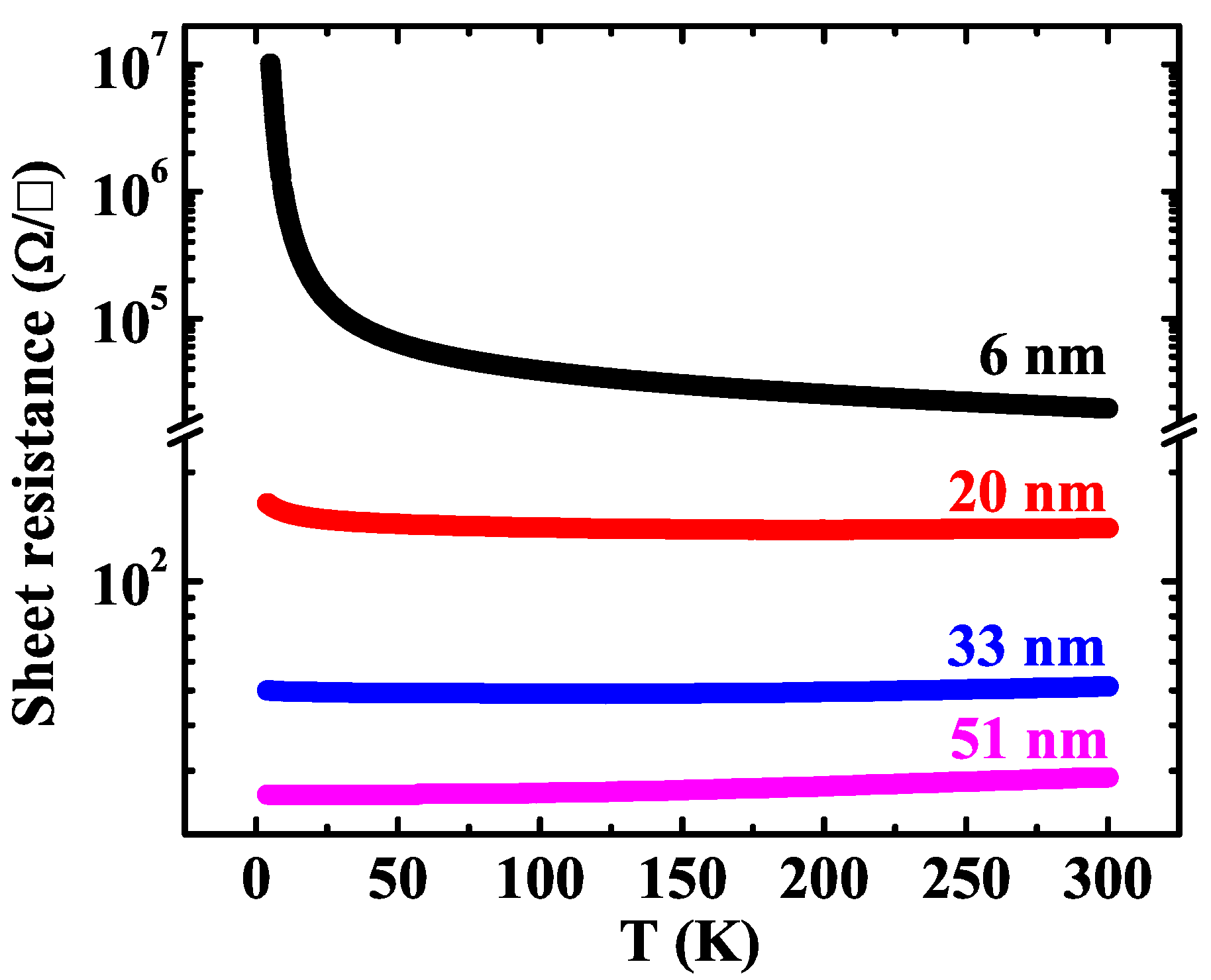
To investigate the thickness driven metal-insulator transition (MIT) in Ga:ZnO films, temperature (T) dependent sheet resistance measurements on all the samples were carried out using standard 4-probe method. Irrespective of T, the sheet resistance () increases as film thickness is reduced. The values of for 51, 33 and 20 nm thick films are 29 , 51 and 140 respectively. With further decrease in film thickness, there is a sharp increase in as shown in Fig. 3. At 300 K, of 6 nm film is found to be 19.7 k . Similar behavior is observed in Si doped ZnO thin films by Das et alDas et al. (2014). Sheet resistance (R), resistivity () and carrier concentration () of Ga:ZnO films measured at 300 K are listed in the Table 1.
| Film thickness (nm) | () | (-cm) | (cm-3) | |
|---|---|---|---|---|
| 51 | 29 | 0.92 | ||
| 33 | 51 | 0.97 | ||
| 20 | 140 | 1.2 | ||
| 6 | 19667 | 0.05 | 188 |
The carrier concentration is found to be and cm-3 for 51 and 6 nm films respectively. Figure 3 depicts the behavior of sheet resistance () as a function of temperature for all Ga:ZnO films of different thickness. We find that there is a weak dependence of on temperature for thicker films (20 nm and above). However, in the case of 6 nm thick film, there is a sharp increase in below 50 K which is the characteristic feature of an insulator.
For further analysis of electrical transport properties, we have plotted resistivity () as a function of temperature as shown in Fig. 4. At 300 K, of the 51 nm thick film is found to be 0.66 m-cm which is very close to the earlier reportsBhosle et al. (2006). For 33 and 20 nm films, at 300 K is 0.77 and 1.3 m-cm respectively. Figures 4(a) and (b) display the plot of as a function of temperature for 33 and 20 nm films. As temperature is lowered down from 300 K, decreases and reaches to a minimum value. On further reduction in temperature below the transition temperature (TMIT), increases. The resistivity minimum is generally observed in degenerate semiconductorsDas et al. (2014). Both the samples show positive temperature coefficient of resistivity (TCR) at high temperature regime and below the TMIT, TCR becomes negative. Transition temperature (TMIT) is observed at 125 K and 190 K for the films with thickness 33 and 20 nm respectively. It should be noted that TMIT increases as the film thickness is reduced. The negative TCR below the TMIT can be explained with the frame of weak localization (WL) phenomena. In the case of weak localization, due to quantum interference, the electronic wave functions diffuse and thereby enhance the backscattering which in turn increases the resistivity.
The conductivity in the weak localization regime for a 2D system is given as Lee and Ramakrishnan (1985); Scherwitzl et al. (2011),
| (1) |
where, is Drude conductance and is a parameter that depends on the nature of inelastic dephasing mechanism. The value of is one for electron-electron collision and 3 for electron-phonon collisionScherwitzl et al. (2011). The constant is related to the mean free path for elastic collision. Insets of Fig. 4 (a) and (b) displays the vs. plot of the 33 nm and 20 nm films at low temperature regime (TMIT) respectively.
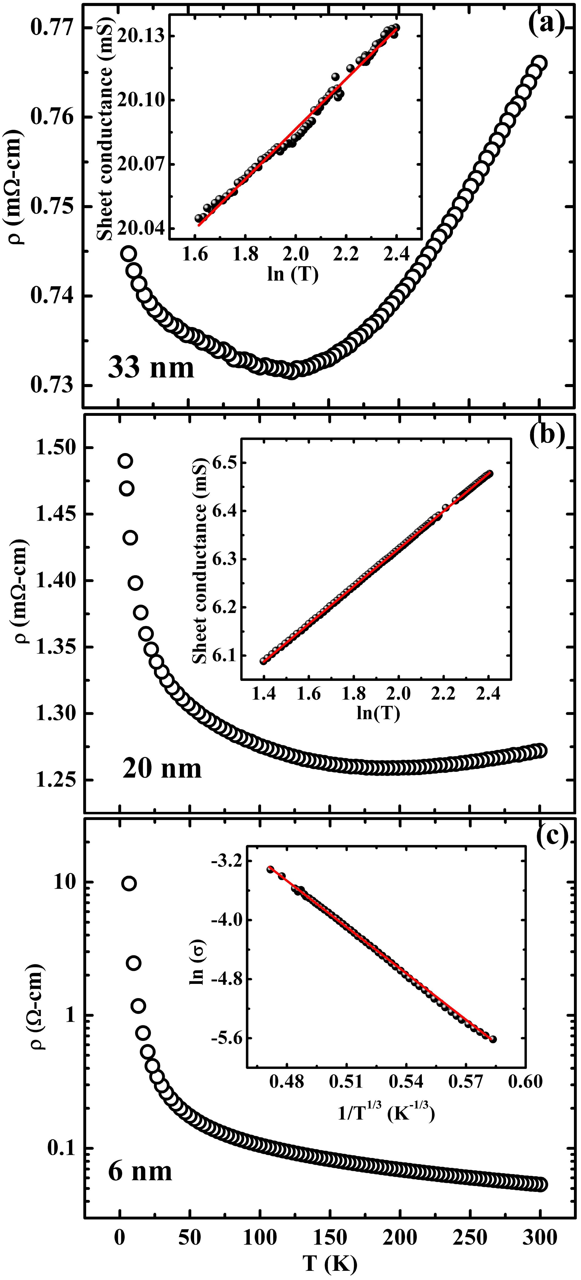
The linear behavior of with can be observed from these insets. The slopes are found to be and for the 33 nm and 20 nm samples respectively. Therefore, we infer that the transport follows the 2D weak localization behavior in these samples. The resistivity value and the positive TCR suggests that the films with thickness 20 nm and above exhibits metallic type conduction. Moreover, the resistivity at 5 K and 300 K are very close in these samples which also indicate a metallic type behaviorMukherjee and Rao (2017).
The temperature dependent resistivity plot of 6 nm thick film is reverse to the trend shown by thicker samples. From Fig. 4(c) we observe negative temperature coefficient of resistivity (TCR) throughout the temperature range which conclusively predicts the insulating behavior. The slope at low temperature regime ( K) is higher than the high temperature regime as can be realized from Fig. 4(c). The two different slopes can be attributed to the two different conduction mechanisms present in the two different temperature scales. Generally at high temperature regime, the transport is mainly governed by thermally activated band conduction. For thermally activated band conduction, the conductivity is given by where, is the pre-exponent factor, is the activation energy. The Arrhenius fitting of the conductivity data yields the activation energy as 27 meV. Resistivity sharply increases at the low temperature regime below 50 K. At low temperature, the thermal energy is insufficient to activate the carriers. Therefore, the conduction process mainly takes place through the variable range hopping mechanism. In this process electrons can hop from one site to other sites that are close to the Fermi level irrespective of their spatial separation. The relation between electrical conductivity and temperature for VRH mechanism in 2D system is given byStepina et al. (2009),
| (2) |
where, is a pre-exponent constant and is the characteristic temperature. Inset of Fig. 4(c) displays the variation of vs. of 6 nm thick sample in the temperature range of 50 to 10 K. The linear fitting (red solid line in Fig. 4(c)) of the plot indicates that the VRH mechanism is dominant in the conduction below 50 K.
III.4 Magnetoresistance
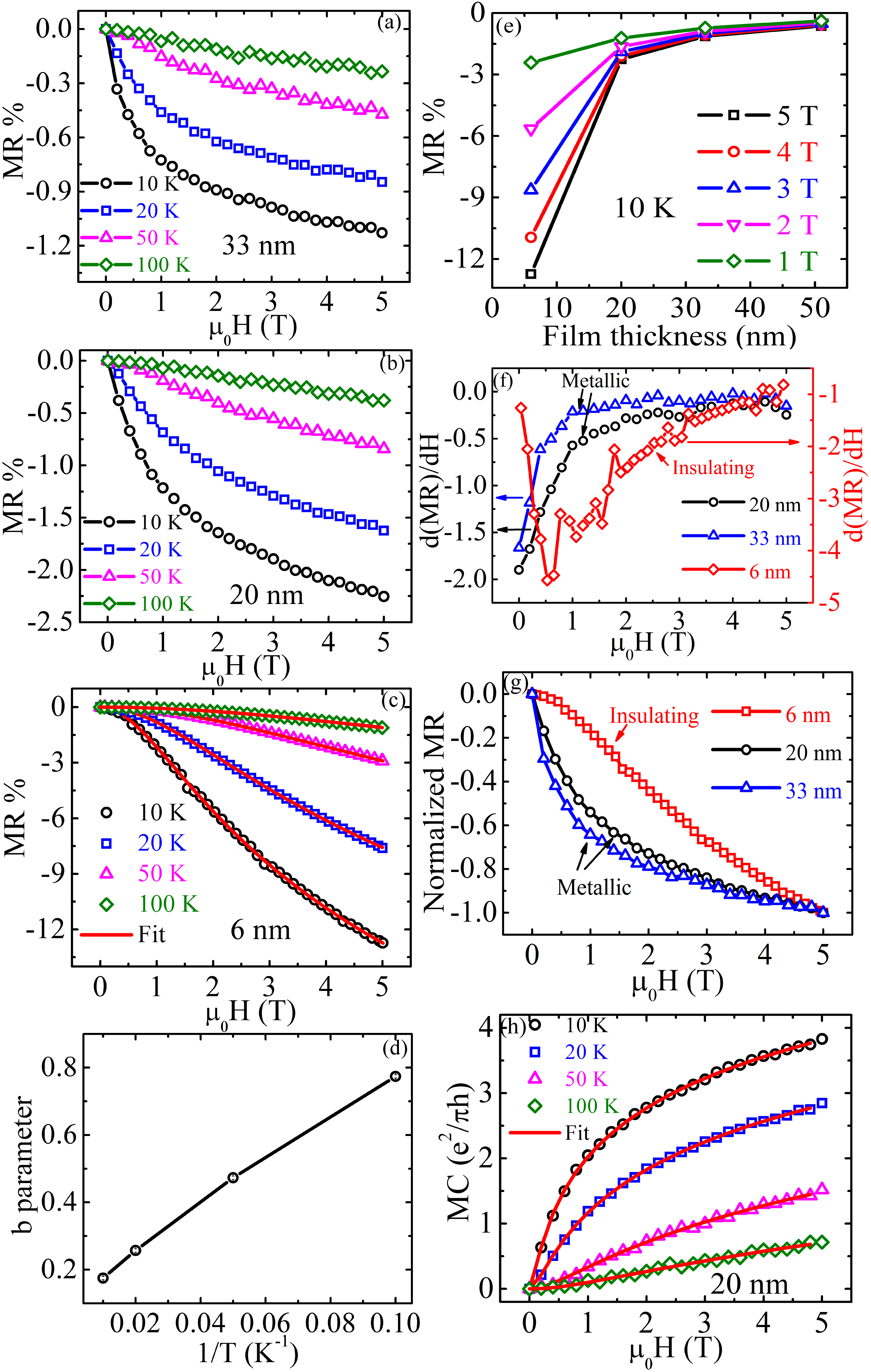
The resistivity data discussed in the last section not only infers metal insulator transition (MIT), but also it provides indication of strength of electron localization. The resistivity data of 6 nm film fits well with the proposed VRH model suggesting strong localization (SL). At the same time, the small upturn at low temperature regime for thicker (20 nm and above) films hints toward weak localization (WL) which agrees well with 2D WL model. In order to substantiate the MIT and to verify the nature of localization inferred from the resistivity data, we have carried out magnetoresistance measurement and the results are displayed in Fig. 5. As expected, from Fig. 5 (a-c), we find that irrespective of the film thickness, the MR became more negative with decrease in temperature. The negative MR has been observed on Ga doped ZnO thin films by Reuss et alReuss et al. (2005). While the MR vs. H is qualitatively similar, there is a large quantitative difference between metallic and insulating samples. As film thickness decreases, magnitude of MR increases which can be realized from Fig. 5(e). At 10 K with 5 T field, the maximum MR observed in 20 and 33 nm thick samples is 1.3 and 2.4 % respectively. Generally, in WL regime, a small magnitude (1-2 %) of MR is observed due to the suppression of WL in the presence of magnetic fieldAndrearczyk et al. (2006); Mukherjee and Rao (2017).
To understand the variation of MR on applied magnetic field, we have plotted (d(MR)/dH) and normalized MR in Figs. 5(f) and (g) respectively. From the normalized plot, it can be observed that for the metallic samples, the magnitude of MR increases sharply at low field regime ( T). Therefore, we observe a large value of d(MR)/dH at small H (see Fig. 5(f)). On further increase in field strength, d(MR)/dH approaches to saturation indicating smaller and constant change in MR with field. This is because a small magnetic field can suppress the weak localization effectMukherjee and Rao (2017). Further increasing the field strength yields a lower change in MR. Therefore, the change in MR with respect to the field is more prominent at low magnetic field compared to the higher field. To fit the experimental data, we have applied 2D WL model for 20 nm and above thick films. We have calculated the magnetoconductance (MC) for the metallic samples defined as . In these samples, temperature dependent resistivity measurement confirmed the presence of weak localization at low temperature regime. In 2D system, MC due to weak localization effect is given by Lee and Ramakrishnan (1985); Scherwitzl et al. (2011),
| (3) |
where, is electronic charge, is the Planck’s constant, is Digamma function. The term is defined as where, is the inelastic scattering length. The magnetoconductance data of Ga:ZnO films with thickness 20 nm and above are fitted to the Eq. (3). Figure 5(h) shows magnetoconductance behavior of 20 nm thick film. It can be observed that the experimental data is well agreed with the 2D WL model. The inelastic scattering length was found to be 65 nm at 10 K and 15 nm at 100 K in this film.
Unlike to the metallic samples, the MR of 6 nm thick sample is different in two aspects. First the magnitude is much larger than that of metallic samples and the dependence of MR on H is also different. A maximum value of 12.7 % MR is observed in 6 nm thick sample which shows strong localization behavior in the resistivity measurement. This magnitude of MR agrees with the MR observed in other doped ZnO films exhibiting strong insulating behaviorAgrawal et al. (2014); Mukherjee et al. (2017). For insulating sample d(MR)/dH vs. H curve exhibits a minimum at a magnetic field of 0.5 T at 10 K. Similar behavior is observed in La0.7Ca0.3MnO3 system in the insulating regimePękała et al. (2008). Below this minimum ( T), magnitude of d(MR)/dH increases with field. After reaching the maximum, the magnitude of d(MR)/dH decreases which indicates a slower rate of MR with field. In strong localization limit negative MR is explained by the scattering center. Upon application of a magnetic field, scattering centers align among themselves. As, a high field is required to align the scattering centers, d(MR)/dH first increases with field and after reaching the maximum value it starts decreasing. It has been observed by manyMukherjee et al. (2017) that in the strong localization regime, negative MR follows the semi-emperical Khosla-Fischer modelKhosla and Fischer (1970). We have analyzed the MR data of 6 nm thick film with a semi-empirical model proposed by Khosla and Fischer. According to this model, negative MR is given byKhosla and Fischer (1970),
| (4) |
The parameters a and b are defined as
| (5) |
and
| (6) |
where constant is a measure of spin based scattering, is the exchange integral, is the density of states at the Fermi energy, is the spin of the localized moment, is the average magnetization, is the g-factor and is a numerical constant. The MR data of 6 nm thick Ga:ZnO film was fitted using the Eq. (4). Figure 5(c) suggests that experimental data are in good agreement with the Khosla and Fischer model. The fitting parameter is plotted in Fig. 5(d) and it varies inversely with temperature as expected from Eq. (6)Gacic et al. (2007). The other parameter slightly decreases with temperatureMukherjee et al. (2017); May et al. (2004); Peters et al. (2010).
IV Lattice disorder and electronic structure
To examine the electronic contribution to the transport properties of Ga:ZnO film, in this section we analyzed the band structure of this doped system obtained from the DFT calculations. While experimentally synthesized samples have 1 Ga doping, due to computational limitations, theoretical studies are performed with 3 Ga doping. The doping is realized by replacing one Zn atom by Ga in a supercell as shown in Fig. 6(a). Also due to computational limitations, calculations are performed only on bulk Ga:ZnO and two unit cell thick (1 nm) film along (001) (see Fig. 6(e)). While the former can represent the experimentally synthesized thicker films, the latter closely stands for the 6 nm thin film. The film was constructed by introducing 15 Åvacuum on the surface of 2 unit cell thick supercell as shown in the Fig. 6(e). The ground state structure is realized through complete relaxation of the experimental structure of bulk ZnOSans et al. (2009).
The calculations are carried out using the Vanderbilt ultra-soft pseudopotentialVanderbilt (1990) and plane wave basis sets as implemented in Quantum EspressoGiannozzi et al. (2009) and within the frame work of PBE-GGA exchange correlation approximationPerdew et al. (1996). The kinetic energy cutoff to fix the number of plane waves is taken as 30 Ry. The Brillouin zone integration is performed using the Gaussian method on a k-grid for bulk and k-grid for film.
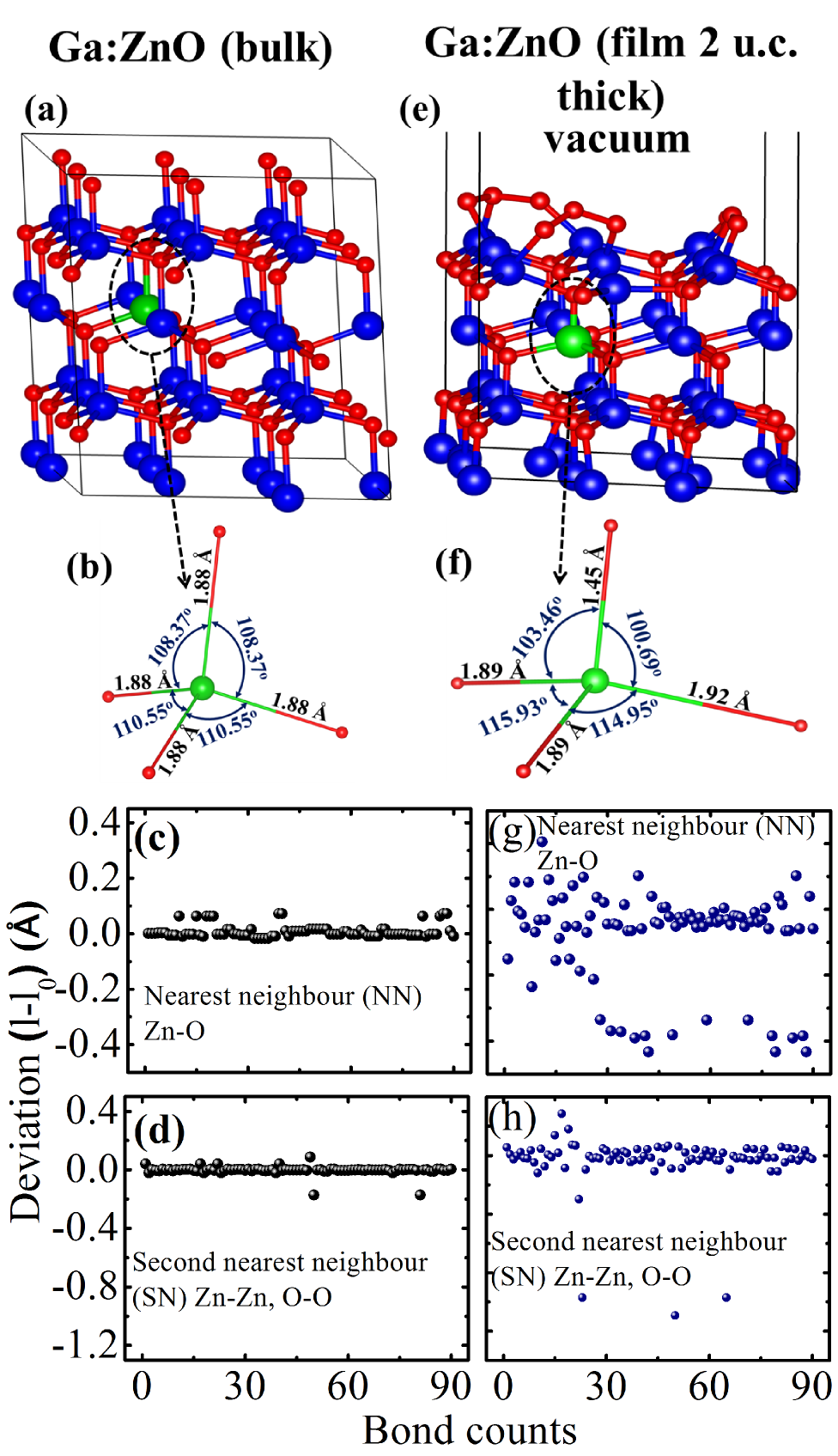
With introduction of impurities (vacancy, dopant etc.), crystalline disorder occurs and the extent of disorderness primarily depends on the charge state and ionic radii of the impurities. Subsequently, the disorder introduces new localized states and thereby alters the transport properties of the compound. To explain this aspect, we have measured the crystalline disorder of Ga:ZnO both in bulk and thin film. The results are shown in Fig. 6. Figures 6(a) and (e) respectively show the fully relaxed structure of bulk and film and it is visible that in film disorder is more than that in the bulk. Moreover, from Fig. 6(b) we find that for bulk Ga:ZnO, the impurity Ga-O bond in the nearest neigborhood is isotropic with length 1.88 Å. However, in the case of film (see Fig. 6(f)), the Ga neighborhood is highly anisotropic with Ga-O bond length varies from 1.45 to 1.92 Å.
To provide a quantitative measure of disorderness in the doped system, we estimated the deviation of nearest neighbor (NN) and second neighbor (SN) bond length from that of the undoped bulk ZnO. The results are presented in Figs. 6(c-d) and 6(g-h). We find that out of 64 possible NN bonds, a maximum of 7 bonds are deviated by 0.1 Åfrom the original value in the case of bulk compound. However, in the case of film nearly 56 bonds are deviated significantly and the deviation lies in the range of -0.5 to 0.2 Å. The same can be realized from the SN bond lengths even though the number of deviations is comparatively less. Therefore, collectively we find that the extent of disorder in film is significant and likely to impact the transport properties which can be understood from the band structure and density of states.
ZnO is a known semiconductor with the Fermi level lies between the occupied O-p dominated valence bands and Zn-4s dominated dispersive conduction band. Figure 7 (a) shows the band structure of pure ZnO plotted using the Brillouin zone of a 332 supercell. The lower conduction band is highly dispersive and with a large band width of 7 eV. Due to band folding this band consists of several subbands which are degenerate along A-L and also at H. With Ga doping, both the orbital and crystal symmetry break along with a minor crystal disorder which is discussed in Fig. 6. Such disorder and symmetry breaking lead to the lifting of the subband degeneracy (See the band dispersion in the range 1-3 eV for pure and -0.5 to 1 eV for doped sytem with respect to EF) which can be seen from Fig. 7(b). Now the Ga-p dominated lower subband, which is parabolic with width 2 eV and separated from the upper subbands of the conduction spectrum, is partially occupied to make the system a n-type degenerate semiconductor. The parabolic behavior of the impurity band is in good agreement with our experimental study where we have shown that the thickest film (51 nm) exhibits positive temperature coefficient of resistivity like a metal. The density of states in Fig 7(b) reflects the same where the tail of the conduction band is smooth and well below EF.
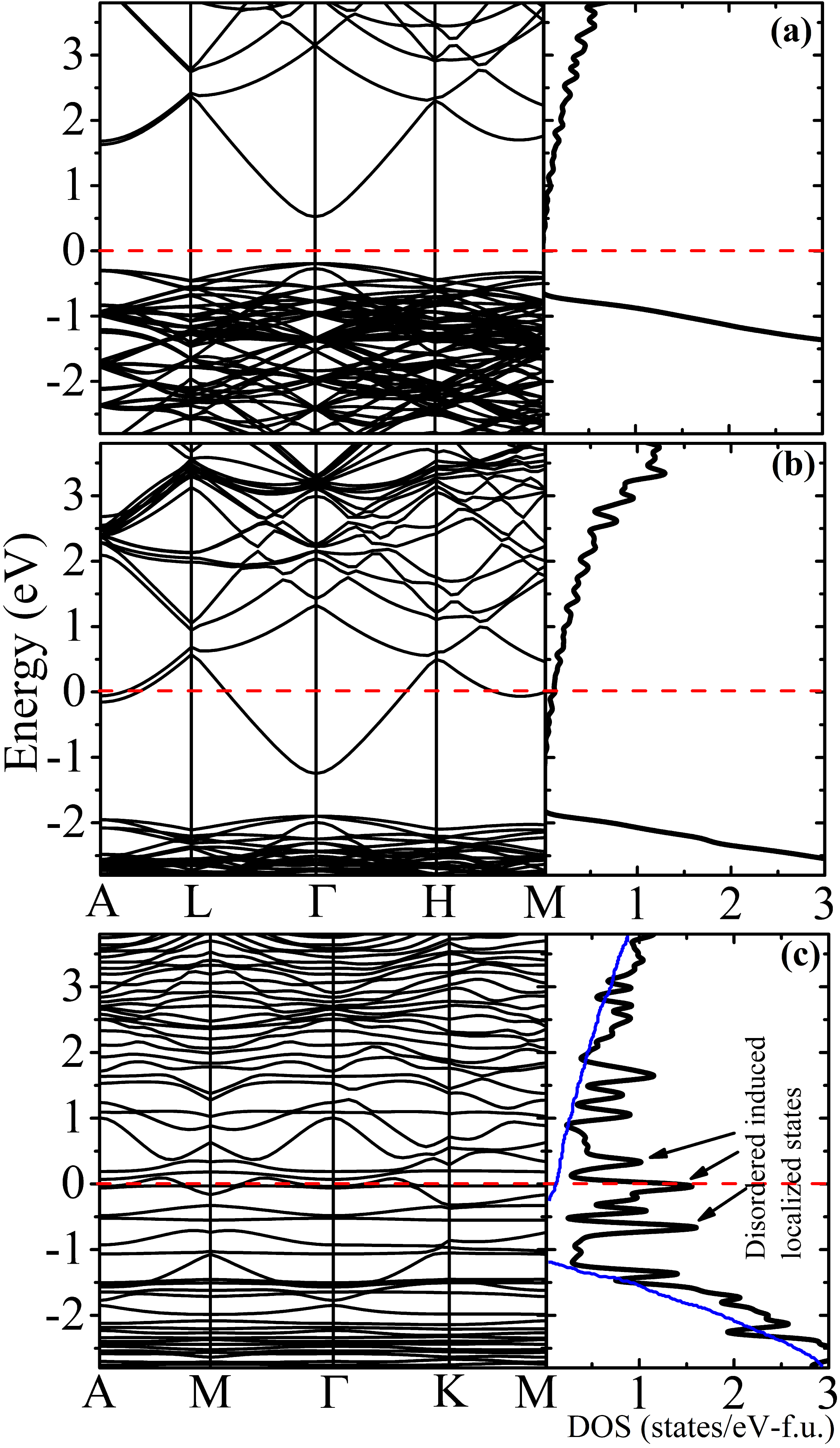
As discussed earlier, the crystalline disorder in film is very profound in the film. As a consquence, the bulk covalent band gap disappears. Instead several localized state appears below and above EF as can be seen from the bands and DOS of Fig 7(c). Since, one electron is donated by Ga, it is natural to see a partially occupied band. Howevere, unlike to the bulk case, such a band is of narrow band width due to localization effect. From Fig. 7(c) we observe that the band width of this partially occupied band is approximately 0.2 eV which is almost one order less than that of the doped bulk system signifying the strength of the crystal disorder.
In earlier studies on hydrogenated amorphous SiMott (1980)Okamoto and Hamakawa (1977), such localized states in the vicinity of the EF have been found. These states are reported to be responsible for the insulating behavior, mediated through the VRH mechanism, of these compounds. The localized states of Ga:ZnO film here resembles to that of amorphous Si and favor the insulating behavior. The experimentally observed insulating behavior of 6 nm film resonates with the lattice disorder led insulating phenomena of 2 unit cell thick film. We may note that Fig. 2 indicates a broad peak in the XRD pattern of the 6 nm film as opposed to the narrow peaks shown by the 20 nm and above thicker films.
V Summary and conclusions
To sumarize, structural, electrical and magnetotransport properties of PLD grown Ga doped ZnO thin films were extensively studied and analyzed. Metal-insulator transition was observed as a function of the film thickness. While the sample with thickness of 20 nm and above exhibits metallic type of conduction, the film of 6 nm thick is found to be insulating. Temperature dependent resistivity and magnetoresistance measurements further confirm the presence of weak localizatin in 20 nm and above thicker samples. However, strong localization is observed in 6 nm thick film as resistivity data follow Mott-VRH model. Moreover, the magnetoresistance data is well matched with Khosla-Fischer model to further substantiate the strong localization behavior in 6 nm film. Our structural relaxation calculations, carried out using density functional theory, suggests that the dopant as well surface reconstruction introduce larger disorder in thinner samples. As a consequence, the system has disorder induced localized states in the vicinity of Fermi level. The donor electrons occupy some of these localized states to weaken the mobility and exhibit insulating behavior.
Acknowledgements.
Authors thank Department of Science and Technology (DST), New Delhi, that facilitated the establishment of “Nano Functional Materials Technology Centre” (Grant: SRNM/NAT/02-2005). J. M. thanks Mr. Ajit Jana for his help in DFT calculations. Institute HPCE facility was used for the computations. J. M. wants to thank UGC for SRF grant.References
- Chu et al. (2008) S. Chu, M. Olmedo, Z. Yang, J. Kong, and J. Liu, Applied Physics Letters 93, 181106 (2008), http://dx.doi.org/10.1063/1.3012579 .
- Choi et al. (2010) Y. S. Choi, J. W. Kang, D. K. Hwang, and S. J. Park, IEEE Transactions on Electron Devices 57, 26 (2010).
- Chu et al. (2011) S. Chu, G. Wang, W. Zhou, Y. Lin, L. Chernyak, J. Zhao, J. Kong, L. Li, J. Ren, and J. Liu, Nature nanotechnology 6, 506 (2011).
- Minami (2000) T. Minami, MRS Bulletin 25, 38–44 (2000).
- Bhosle et al. (2006) V. Bhosle, A. Tiwari, and J. Narayan, Journal of Applied Physics 100, 033713 (2006), http://dx.doi.org/10.1063/1.2218466 .
- Kuznetsov et al. (2015) V. L. Kuznetsov, A. T. Vai, M. Al-Mamouri, J. S. Abell, M. Pepper, and P. P. Edwards, Applied Physics Letters 107, 232103 (2015), http://dx.doi.org/10.1063/1.4936613 .
- Das et al. (2014) A. K. Das, R. S. Ajimsha, and L. M. Kukreja, Journal of Applied Physics 115, 193705 (2014), http://dx.doi.org/10.1063/1.4878698 .
- Sans et al. (2009) J. A. Sans, J. F. Sánchez-Royo, A. Segura, G. Tobias, and E. Canadell, Phys. Rev. B 79, 195105 (2009).
- Look et al. (2011) D. C. Look, K. D. Leedy, L. Vines, B. G. Svensson, A. Zubiaga, F. Tuomisto, D. R. Doutt, and L. J. Brillson, Phys. Rev. B 84, 115202 (2011).
- Snure and Tiwari (2007) M. Snure and A. Tiwari, Journal of Applied Physics 101, 124912 (2007), http://dx.doi.org/10.1063/1.2749487 .
- Dong et al. (2007) B.-Z. Dong, G.-J. Fang, J.-F. Wang, W.-J. Guan, and X.-Z. Zhao, Journal of Applied Physics 101, 033713 (2007), http://dx.doi.org/10.1063/1.2437572 .
- Opel et al. (2014) M. Opel, S. Geprägs, M. Althammer, T. Brenninger, and R. Gross, Journal of Physics D: Applied Physics 47, 034002 (2014).
- Lee and Ramakrishnan (1985) P. A. Lee and T. V. Ramakrishnan, Rev. Mod. Phys. 57, 287 (1985).
- Scherwitzl et al. (2011) R. Scherwitzl, S. Gariglio, M. Gabay, P. Zubko, M. Gibert, and J.-M. Triscone, Phys. Rev. Lett. 106, 246403 (2011).
- Mukherjee and Rao (2017) J. Mukherjee and M. S. R. Rao, Applied Physics Letters 110, 122101 (2017), http://dx.doi.org/10.1063/1.4978530 .
- Stepina et al. (2009) N. P. Stepina, E. S. Koptev, A. V. Dvurechenskii, and A. I. Nikiforov, Phys. Rev. B 80, 125308 (2009).
- Reuss et al. (2005) F. Reuss, S. Frank, C. Kirchner, R. Kling, T. Gruber, and A. Waag, Applied Physics Letters 87, 112104 (2005), http://dx.doi.org/10.1063/1.2045553.
- Andrearczyk et al. (2006) T. Andrearczyk, J. Jaroszyński, G. Grabecki, T. Dietl, T. Fukumura, and M. Kawasaki, physica status solidi (c) 3, 1030 (2006).
- Agrawal et al. (2014) A. Agrawal, T. A. Dar, P. Sen, and D. M. Phase, Journal of Applied Physics 115, 143701 (2014), http://dx.doi.org/10.1063/1.4870864.
- Mukherjee et al. (2017) J. Mukherjee, R. Mannam, and M. S. R. Rao, Semiconductor Science and Technology 32, 045008 (2017).
- Pękała et al. (2008) M. Pękała, N. Kozlova, and V. Drozd, Journal of Applied Physics 104, 123902 (2008), http://dx.doi.org/10.1063/1.3040013 .
- Khosla and Fischer (1970) R. P. Khosla and J. R. Fischer, Phys. Rev. B 2, 4084 (1970).
- Gacic et al. (2007) M. Gacic, G. Jakob, C. Herbort, H. Adrian, T. Tietze, S. Brück, and E. Goering, Phys. Rev. B 75, 205206 (2007).
- May et al. (2004) S. J. May, A. J. Blattner, and B. W. Wessels, Phys. Rev. B 70, 073303 (2004).
- Peters et al. (2010) J. A. Peters, N. D. Parashar, N. Rangaraju, and B. W. Wessels, Phys. Rev. B 82, 205207 (2010).
- Vanderbilt (1990) D. Vanderbilt, Phys. Rev. B 41, 7892 (1990).
- Giannozzi et al. (2009) P. Giannozzi, S. Baroni, N. Bonini, M. Calandra, R. Car, C. Cavazzoni, D. Ceresoli, G. L. Chiarotti, M. Cococcioni, I. Dabo, A. D. Corso, S. de Gironcoli, S. Fabris, G. Fratesi, R. Gebauer, U. Gerstmann, C. Gougoussis, A. Kokalj, M. Lazzeri, L. Martin-Samos, N. Marzari, F. Mauri, R. Mazzarello, S. Paolini, A. Pasquarello, L. Paulatto, C. Sbraccia, S. Scandolo, G. Sclauzero, A. P. Seitsonen, A. Smogunov, P. Umari, and R. M. Wentzcovitch, Journal of Physics: Condensed Matter 21, 395502 (2009).
- Perdew et al. (1996) J. P. Perdew, K. Burke, and M. Ernzerhof, Phys. Rev. Lett. 77, 3865 (1996).
- Mott (1980) N. F. Mott, Journal of Physics C: Solid State Physics 13, 5433 (1980).
- Okamoto and Hamakawa (1977) H. Okamoto and Y. Hamakawa, Solid State Communications 24, 23 (1977).