Extraction of built-in potential of organic diodes from current-voltage characteristics
Abstract
Physics based analytic equations for charge carrier profile and current density are derived by solving the carrier transport and the continuity equations for metal-intrinsic semiconductor-metal diodes. Using the analytic models a physics based method is developed to extract the built-in potential from current density-voltage (-) characteristics. The proposed method is thoroughly validated using numerical simulation results. After verifying the applicability of the proposed theory on experimentally fabricated organic diodes, is extracted using the present method showing a good agreement with the reported value.
keywords:
Organic diode , Organic solar cell , Device simulation , Built-in potential , Injection limited current , Space charge limited current1 Introduction
In organic diodes and solar cells, organic semiconductors are typically sandwiched between two dissimilar metal electrodes. The electric field and the charge profile under equilibrium are governed by the metal contacts of these devices. Moreover, the work function difference of the electrodes determines [1], which is a crucial metric for both organic diode and solar cells as far as device performance is concerned. However, the charges that get injected from the contacts cause an excess potential drop near the metal-semiconductor junctions [2]. This excess drop in potential leads to a reduction of [3] to a lower value, say , which is typically measured instead of for a given temperature .
In this work we propose a physics-based analytical model for estimating from - characteristics which takes the effect of injected charge into account. Our model is further extended to establish a method for extracting by using dependency of . Finally, the method is employed to estimate of poly(3-hexylthiophene) (P3HT):phenyl-C61-butyric acid methyl ester (PCBM) based organic diodes, which are fabricated in our laboratory.
2 Simulation and analytical results
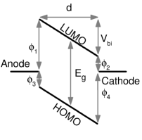
We use the Metal-Insulator-Metal methodology for numerical simulation [4, 5, 6]. The numerical simulations are done using the commercially available the Sentaurus technology computer-aided design (TCAD) tool [7]. In numerical simulations, we consider Schottky contacts at anode and cathode with barriers (), () for electrons (holes) respectively [Fig. 1].
Therefore the carrier concentrations at the contacts are determined by thermionic emission process and are given as
| (1) |
where is the thermal voltage, , are the electron (hole) concentration at anode and cathode respectively, () is the effective density of states for electrons (holes).
2.1 Classification of diodes
At equilibrium (applied voltage V ) the dissimilar metal work-functions are aligned leading to band bending [Fig. 1] which sets up a built-in electric field inside the device. The strength of the built-in electric field depends on , d and the injected charge. Depending on the magnitude of the injected charge and its effect on the electric field, the diodes can be classified into two categories: (1) Low space charge (LSC) case. (2) High space charge (HSC) case. The injected charge can be modified by changing (), barrier for electrons (holes) and the temperature. In this particular study we keep () unchanged and vary the barriers for electrons (holes) and the temperature to explain LSC and HSC cases. The parameters associated with the simulation for LSC and HSC cases are given in Fig. 2.
2.1.1 Low Space Charge case
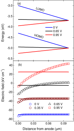
In LSC case, the field due to the injected charge is very less compared to the electric field generated due to work-function difference. Hence the electric field is expected to be uniform by maintaining linear band bending [Fig. 2(b)] inside the device [Fig. 2(a)]. The injected carriers (from metals) undergo diffusion and drift concurrently in opposite direction to each other, as a consequence of concentration gradient and electric field respectively. Thus in order to model the carrier profiles and the current density, both drift and diffusion have to be considered simultaneously. The transport equation, describing electron current density, can be expressed as
| (2) |
where is the electron charge, is the electric field, is the electron carrier concentration and is the mobility of electron. As discussed above, is uniform and it is represented as
| (3) |
In order to arrive at analytic solution under steady state conditions, we consider three assumptions: (1) Semiconductor is intrinsic, (2) Carrier mobilities ( and hole mobility ) are constant with respect to and , (3) There is no carrier generation and recombination. The last assumption modifies the continuity equation for electrons as
| (4) |
Using Eqs. (2), (3) and (4), a second order differential equation is developed for as
| (5) |
By employing the thermionic emission boundary condition for electrons [Eq. 1], an analytic solution for is obtained as
| (6) |
Similar approach can be used to obtain an analytic solution for holes.
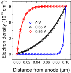
The extracted electron profile inside the device using TCAD simulation (symbols) and Eq. 6 (solid lines) for different are compared in Fig. 3 which ensures that Eq. 6 is in good agreement with the TCAD results. Further, the analytic solution for current density can be expressed using Eqs. (2), (3), (6) and their hole counterparts as
| (7) |
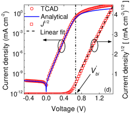
The variation of with respect to , based on TCAD simulation (symbols) and Eq. 7 (solid line) are displayed in Fig. 4, showing excellent consistency. A similar equation has been reported by different groups in the literature [4, 8]. Where S Jung et al. arrived at a similar analytical equation for less disordered organic materials with Gaussian density of states. However, the present method is completely rest upon charge based model with coherent device physics considering the effective density of states.
According to Fig. 3, charge increases exponentially from anode to cathode for (0.7 V in particular). The exponential nature of charge along with linear variation of with results in exponential variation of with respect to . On the other hand, for , the charge carrier profile changes significantly [Fig. 3] by virtue of field reversal [Fig. 2]. Charge carrier concentration increases from anode to cathode like a logistic function [Fig. 3], maintaining its spatially uniform nature inside the device except near the anode-semiconductor junction. The uniform nature of both charge carrier concentration and electric field profiles leads to a linear variation of current. In LSC case, the current is typically injection limited current (ILC) since dominant part of the current is controlled by the injected charge carriers.
2.1.2 High Space Charge case
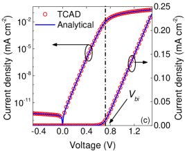
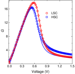
In HSC case, the electric field due to the injected charge becomes comparable to the electric field associated with band bending, expressed by Eq. 3. Hence the net electric field within the device becomes non-uniform. HSC case can be realized by reducing the barrier height for electrons (holes) or by increasing () or by increasing the thickness of the semiconductor. However, in this study HSC is realized by reducing the barrier height at anode-semiconductor junction in particular. Under equilibrium, a uniform electric field is observed within the device except near the anode-semiconductor junction where injected charge is high [Fig. 2(b)]. However, for the magnitude of uniform electric field is slightly less than that of LSC case. Thus, - characteristics maintain the same exponential nature as that of LSC case, exhibiting a reduction in built-in potential [Fig. 5]. Hence it is essential to modify the electric field in case of HSC by reducing to (i.e., ) where accounts for the reduction in due to the injected charge. However, in case of , the non-linearity in electric field profile near the anode-semiconductor junction becomes predominant upon applying voltage and spreads throughout the device differing drastically from that of LSC case. As a consequence, the electric field and the carrier concentration become interdependent, leading to non-linear - characteristics. The current density varies with square of (for ) as evidenced by a linear nature of -V characteristics [Fig. 5]. As the current is controlled by the space charge, it is space charge limited current (SCLC).
2.2 Extraction of Built-in potential
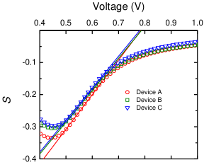
In LSC case, changes its nature from exponential to linear for , whereas in HSC case, changes its nature from ILC to SCLC for . Most of the practical organic diodes belong to HSC case. To understand more about current transition from exponential to linear or ILC to SCLC, we adopt a function , proposed by Mantri et al. [9], where is defined as
| (10) |
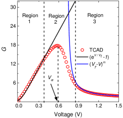
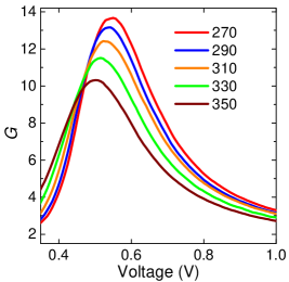
The variation of with respect to shows three distinct regions signifying three different nature of current [Fig. 6]. In region-1, the variation of can be fitted using a simple exponential function of as , as represented by solid line. In region-3, follows a power law as with an exponent m, where and are fitting parameters. Transition between these two regions (1 and 3) occurs through region-2, showing a combined effect of exponential and power law. Moreover, in region-2, - characteristics exhibit a peak at a voltage, termed as . TCAD simulation results for the variation of with respect to temperature as a function of different is depicted in Fig. 7. It emphasizes that modeling variation with will help in determining from - characteristics. Using Eq. (9) and Eq. (10), a unified expression for is developed as
| (11) |
Eq. (11) consists of two terms which correspond to two different nature of current. First term shows exponential nature, whereas the second term represents a power law with and . Eq. (11) shows an excellent match with the TCAD results for LSC case, where [Fig. 8]. In case of HSC, there is indeed a good agreement between Eq. (11) and TCAD results throughout regions 1 and 2. However, - characteristics deviate from Eq. (11) in region-3 due to the presence of SCLC, which cannot be captured by the present model. Thus Eq. 11 is in good agreement with the TCAD results for both LSC and HSC cases throughout region-1 and region-2. Hence Eq. (11) can be used for extracting for both LSC and HSC cases. Using Eq. (11) and equating its first derivative to zero at , we obtain
| (12) |
Eq. (12) can be solved numerically to get . For higher values of , the second term inside the square brackets of Eq. (12) can be neglected. Therefore, a compact analytical equation is realized for as
| (13) |
Subsequently is calculated as
| (14) |
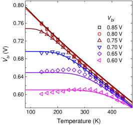
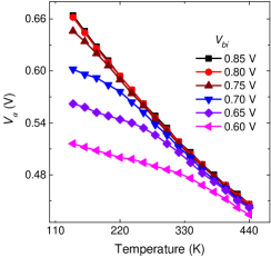
Using Eq. (14) and the value of (extracted from - characteristics), can be calculated. It is evident from Fig. 9 that increases with the decrease in and saturates to . The variation of with respect to arises due to , which in turn depends on dominant injected charge near metal-semiconductor junction [ ] and thereby on . Upon decreasing temperature, the amount of injected charge decreases, resulting tends to be zero and hence approaches to . can be calculated from the relation for different and . From the variation of with respect to , a semi-empirical model is developed for as
| (15) |
where , is the dielectric constant and is a fitting parameter being independent of . Using Eq. (15), can be written as
| (16) |
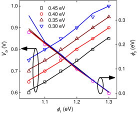
and can be obtained by solving Eq. (16) self-consistently with dependent variation of . The extracted parameters are in good agreement with TCAD results and it is validated for different combinations of and , which shows the robustness of our model [Fig. 10].
3 Experimental results
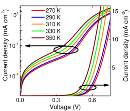
In order to validate our model, is extracted from experimental results of the organic solar cell, fabricated in our laboratory. Organic solar cells consisting of P3HT:PCBM as active material with aluminum (Al) as cathode and indium tin oxide (ITO)/poly(3,4-ethylenedioxythiophene):polystyrene sulfonate (PEDOT:PSS) as anode were fabricated inside a nitrogen glove box and characterized in a vacuum probe station. In order to validate the versatility of our model, we used three different thicknesses, 173 nm (Device A), 154 nm (Device B) and 106 nm (Device C) of P3HT:PCBM, resulting from the spin speed of 850 rpm, 1000 rpm and 1500 rpm respectively. - characteristics of device A as a function of temperature is plotted in semilogarithmic scale and linear scale, as shown in Fig. 11. It is observed that the forward current increases with increase in temperature as expected.
3.1 Model validation for experimental results
To check whether the experimental results follow the proposed model, we have to analyze the variation with for different . For , by considering and using Eq. 1 and Eq. 9 can be written as
| (17) |
where
| (18) |
According to the proposed model varies linearly with with a slope being dependent on . According to Eq. (18), varies linearly with having a slope equal to one and the intercept gives the value of one of the barrier potential ().
| Device | ||||
|---|---|---|---|---|
| (eV) | (V) | (eV) | ||
| A | 0.9903 | 0.8087 | 0.660 | 0.2888 |
| B | 1.006 | 0.7826 | 0.661 | 0.2871 |
| C | 1.004 | 0.7779 | 0.654 | 0.2795 |
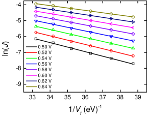
The experimental variation of for Device A (symbols) is shown in Fig. 12 and it confirm the linear variation of with for different applied voltages. Hence the experimental results are fitted with linear variation to find and the intercept and this study is extended for Devices B and C. The variation of with is shown in Fig. 13, one can notice from the figure that for , varies linearly with . Moreover the linear fit in that particular regime gives a slope which is nearly equal to one (Table 1), which is in consistent with the proposed model. Hence this confirm the applicability of the proposed model on these experimental results. In addition we extract one of the barrier potential (or ) for different devices which is nearly equal to eV as tabulated in Table 1.
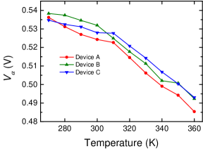
Using Eq. (10), we obtain - plot for Device A, as shown in Fig. 14. is extracted from the peak position of - plot for different temperatures and shown in Fig. 15 for different devices. Subsequently, , calculated using Eq. (12) for devices A,B and C, are shown in Fig. 16 with symbols. As explained earlier, by solving Eq. (16) in coherent manner, and are extracted and presented in the Table 1.
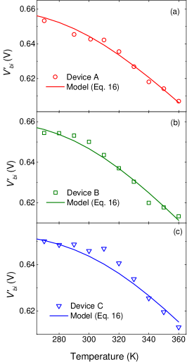
It is important to note that the extracted values of are almost same for different thickness. Hence the obtained using the present model is independent of thickness, as expected. Moreover the extracted values of are in consistent with reported values for P3HT:PCBM device [10], which validates our model and ensures the method of extracting built-in potential from - characteristics of organic diode or solar cell.
4 Conclusion
In summary, we developed analytic models for injected charge profile, - characteristics and . is estimated using temperature dependent variation of . The extracted values of are in good agreement with TCAD results. The extracted from experimental characteristics of P3HT:PCBM based solar cells (organic diode) is in good agreement with the reported values in the literature.
Acknowledgements
The authors would like to acknowledge Department of Science & Technology (DST, Govt. of India), Nissan and IIT Madras for financial support and Centre for NEMS and Nanophotonics (CNNP) for providing fabrication facility.
References
- [1] G. G. Malliaras, J. R. Salem, P. J. Brock, and C. Scott, “Electrical characteristics and efficiency of single-layer organic light-emitting diodes,” Phys. Rev. B, vol. 58, pp. R13411–R13414, Nov 1998.
- [2] J. Simmons, “Theory of metallic contacts on high resistivity solids—i. shallow traps,” J. Phys. Chem. Sol, vol. 32, no. 8, pp. 1987 – 1999, 1971.
- [3] M. Kemerink, J. M. Kramer, H. H. P. Gommans, and R. A. J. Janssen, “Temperature-dependent built-in potential in organic semiconductor devices,” Applied Physics Letters, vol. 88, no. 19, p. 192108, 2006.
- [4] P. de Bruyn, A. H. P. van Rest, G. A. H. Wetzelaer, D. M. de Leeuw, and P. W. M. Blom, “Diffusion-limited current in organic metal-insulator-metal diodes,” Phys. Rev. Lett., vol. 111, p. 186801, Oct 2013.
- [5] G. A. H. Wetzelaer and P. W. M. Blom, “Ohmic current in organic metal-insulator-metal diodes revisited,” Phys. Rev. B, vol. 89, p. 241201, Jun 2014.
- [6] L. J. A. Koster, E. C. P. Smits, V. D. Mihailetchi, and P. W. M. Blom, “Device model for the operation of polymer/fullerene bulk heterojunction solar cells,” Phys. Rev. B, vol. 72, p. 085205, Aug 2005.
- [7] . Sentaurus TCAD Release H-2013.03 Ed.Synopsys Mountain View CA USA
- [8] S. Jung, C.-H. Kim, Y. Bonnassieux, and G. Horowitz, “Injection barrier at metal/organic semiconductor junctions with a gaussian density-of-states,” Journal of Physics D: Applied Physics, vol. 48, no. 39, p. 395103, 2015.
- [9] P. Mantri, S. Rizvi, and B. Mazhari, “Estimation of built-in voltage from steady-state current–voltage characteristics of organic diodes,” Organic Electronics, vol. 14, no. 8, pp. 2034 – 2038, 2013.
- [10] M. Mingebach, C. Deibel, and V. Dyakonov Phys. Rev. B, vol. 84, p. 153201, Oct 2011.