Magnetoelectronic properties of normal and skewed phosphorene nanoribbons
Abstract
The energy spectrum and eigenstates of single-layer black phosphorous nanoribbons in the presence of perpendicular magnetic field and in-plane transverse electric field are investigated by means of a tight-binding method and the effect of different types of edges is analytically examined. A description based on a new continuous model is proposed by expansion of the tight-binding model in the long-wavelength approximation. The wavefunctions corresponding to the flatband part of the spectrum are obtained analytically and are shown to approach agree well with the numerical results from the tight-binding method. Analytical expressions for the critical magnetic field at which Landau levels are formed and the ranges of wavenumbers in the dispersionless flat-band segments in the energy spectra are derived. We examine the evolution of the Landau levels when an in-plane lateral electric field is applied and determine analytically how the edge states shift with magnetic field.
pacs:
71.30.+h, 73.22.-f, 73.63.-bI Introduction
Phosphorene, a single layer of black phosphorus, is a recently isolated material,liu14 ; lu14 providing some extraordinary advantages over other two-dimensional (2D) materials. Most importantly, it has a large band gap of about eV,rudenko15 thus circumventing the main drawback of graphene with its zero band gap. Additionally, because of the puckered structure liu14 ; fei14 ; aierken15 it has highly anisotropic electronic and thermal properties, allowing for the emergence of new functionalities. On top of this, higher carrier mobilities can be achieved as compared to those 2D materials consisting of transition metal dichalcogenides.qiao14
However, phosphorene also has two major downsides: i) the quality of the samples degrades with time when exposed to air,favron14 and ii) unlike few-layer phosphorene the band gap is not electrically tunable. The first issue can be evaded successfully by for instance encapsulating phosphorene with hexagonal boron nitride, which can has the added benefit of increasing the crystal quality and carrier mobility, as in the case of graphene.cao15 ; li15 ; chen15 Besides strain,rodin14 ; cakir14 fashioning phosphorene into nanoribbons can modify the band gap through the quantum confinement effect. Indeed, several theoretical papers have studied various types of phosphorene nanoribbons, and all of them show potentials for certain applications.ezawa14 ; sisakht15 ; grujic16 Note that due to the anisotropy of phosphorene there are two distinct types of zigzag (ZZ) and armchair (AC) edges, normal and skewed, with skewed edges intersecting the ridges of phosphorus atoms at a sharp angle.grujic16 Intriguingly, normal zigzag and skewed armchair (sAC) nanoribbons are metallic, while skewed zigzag (sZZ) and normal armchair nanoribbons are insulating, and all of them have an electrically tunable band structure, featuring metal-insulator transitions for a sufficiently strong electric field.
While it was predicted that ”bulk phosphorene” displays linearly dispersing Landau levels (LLs) for low-energy quasiparticles in low magnetic fields,pereira15 ; ostahie15 ; zhou15 which was confirmed by recent experiments,li15 ; chen15 the results concerning the magnetic response of phosphorene nanoribbons are relatively scarce. In Ref. [zhou15, ] the formation of LLs in normal nanoribbons was reported, while in Ref. [ostahie15, ] the impact of magnetic field on the quasi-flat bands (QFBs) of zigzag nanoribbons were investigated. The purpose of this paper is to examine the influence of magnetic field on phosphorene nanoribbons in more details. In particular, we will examine the band structure of phosphorene nanoribbons with various edge types (including skewed). We will discuss the impact of dispersion anisotropy on LL formation from both the qualitative and quantitative point of view. We will also briefly consider the effect of in-plane electric field on the LLs.
II Theoretical model
We model the phosphorene nanoribbons using the tight-binding model which is defined by hopping parameters rudenko15 which are indicated in Fig. 1. Within the tight-binding approximation the Hamiltonian reads
| (1) |
where the summation runs over all the lattice sites of phosphorene, are the hopping parameters, denotes the Peierls phase picked up while hopping in the presence of the magnetic field, and is the creation (annihilation) operator of an electron on the site j(i).
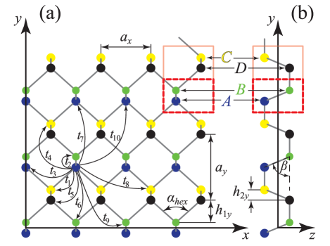
The unit cell of the single phosphorene sheet, framed by the solid square line in Fig. 1, contains four atoms labeled by A (blue), B (green), C (yellow) and D (black). Using the tight binding model, the four-band Hamiltonian ezawa14 ; pereira15 for single-layer phosphorene sheet is given by:
| (2) |
with eigenvectors represented by spinor , and diagonal terms are given by
| (3) |
The interaction terms between sublattice sites are
| (4) | ||||
| (5) | ||||
| (6) |
Here , (see Fig. 1). The parameter values are taken from Ref. [rudenko15, ]. The equality of certain terms of the Hamiltonian (2) indicates the ”equivalence” of certain atomic sites. This is actually due to the point group invariance ezawa14 ; voon15 , which is preserved even when a perpendicular magnetic field is applied. Atoms in the upper and lower lattice, namely and , are ”indistinguishable” and the unit cell is reduced to a single dimmer, framed by the dashed square in Fig. 1. Using this symmetry argument, the simplified two-band Hamiltonian reads
| (7) |
which acts upon the spinors
| (8) |
The eigenvalue problem for the Hamiltonian (7) can be solved analytically
| (9) |
where the upper (lower) sign is for the conduction (valence) band.
Recent theoretical analysis ezawa14 ; pereira15 based on the tight binding model with five hopping parameters shows that the Maclaurin series of analytical functions in the vicinity of the -point up to the quadratic term give satisfactory accuracy for the phosphorene band structure. Using a similar argument we derive the effective two-band Hamiltonian
| (10) |
where , and , with
| (11) | ||||
| (12) | ||||
| (13) | ||||
| (14) | ||||
| (15) | ||||
| (16) | ||||
| (17) |
and obtain the simplified dispersion for electrons and holes
| (18) | |||||
From Eq. (18) it is obvious that, phosphorene has a non-elliptical dispersion due to the parameter .
In order to transform the low-energy Hamiltonian given by Eq. (10) into a more convenient form we perform the unitary transformation given by the Hadamard matrix
| (19) |
The resulting Hamiltonian has the same form as the one obtained in Ref. [rodin14, ] by fitting to results from ab-initio calculations
| (20) |
where diagonal terms
| (21) | |||||
| (22) | |||||
are related to the conduction and valence band dispersions, respectively, while the off-diagonal term introduces interband coupling. Here, are the conduction (valence) band edges in monolayer phophorene, and are the electron and hole effective masses when the coupling is neglected. Furthermore, spinors given by Eq. (8) are transformed to , where .
In the long-wavelength limit . Thus, to lowest order the Eq. (18) is expanded around the -point and the energy dispersions of conduction and valence bands are approximated by and , respectivelyzhou15 . Therefore, the Hamiltonian given by Eq. (20) is reduced to the diagonal form where
| (23) | |||||
| (24) |
The effective masses along the direction remain unchanged,
| (25) |
while the effective masses along the direction are modified by the term that perturbatively takes into account the interband coupling,
| (26) |
The upper ”+” (lower ””) sign is for the electron (hole). The effective masses along the main axes (see Fig. 1) are given in Tab. I. Note that there is a difference between our results and the one obtained from the previously derived continuum model zhou15 based on 5 hopping parametersrudenko14 .
Our goal is to analyze ribbons with arbitrary edges, where the translation vector of a unit cell is
| (27) |
Here, and are mutually prime integers, are the unit vectors, while is the length of the unit cell. Since ribbon edges are not flat, we define the effective ribbon width as the total square of hexagonal plaquettes inside the unit cell divided by the unit cell width .
| -ZZ | -AC | |
| (the electron) | ||
| (the hole) | ||
| ♣results from Ref. [zhou15, ] |
It is straightforward to show that the effective masses of electrons and holes in the vicinity of the -point along the and axes, which are directed along and perpendicular to the ribbon edge, respectively, can be estimated as:
| (28) | |||
| (29) |
Here is the angle of rotation with respect to the coordinate system shown in Fig. 1. In order to write the Hamiltonian in the rotated frame we substitute
in Eqs. (23) and (24). For infinitely long nanoribbons with arbitrary edges the Hamiltonian should not depend on , therefore . For convenience we set in the middle of the ribbon.
We include the magnetic field perpendicular to the structure (). One may show that in the continuum model , where we adopt the Landau gauge , with being the magnetic field length and operators and . Using Eqs. (28,29) and after some elaborate algebra we obtain a set of decoupled differential equations for the conduction and valence band,
| (30) |
where the subscripts and are used for the conduction band, and and denote the valence band. Here, is the shifted coordinate, are the cyclotron frequencies for the electron (hole) in bulk phosphorene, and are eigenenergies measured from the bottom (top) of the conduction (valence) band edges. One may notice that the above equation does not include the term related to the band offset at the edges of the ribbon. This is because we want to analyze the conditions under which LLs exist in a ribbon. Namely, we insist that, either the ribbon is sufficiently wide, or the magnetic field is sufficiently strong, so that particle localization is governed by the effective parabolic potential given in Eq. (30), rather than by the ribbon edges.
We seek the eigenvector components in the form
| (31) |
which leads to the differential equation
| (32) |
where is the dimensionless coordinate and is the dimensionless energy. Finally, to get eigenvalues denoted by the integer quantum number we impose the condition . Thus, the solutions of Eq. (32) are Hermite polynomials
| (33) |
where the principle quantum number is the LL number, the normalization constant is , and the eigenvalues of the LLs follow the quantization of a one-dimensional quantum harmonic oscillator (QHO)
| (34) | |||||
| (35) |
It is obvious that the separation between adjacent energy levels () is approximately . This energy difference is the same for ribbons independent of edges and is equal to the one found in single-layer phosphorous sheetzhou15 ; pereira15 .
It should be pointed out that the exact treatment of LLs in bulk phosphorene shows that the off-diagonal terms, that accounts for the conduction and valence band coupling, are similar in form as the Rasshba (Dresselhaus) spin-orbit interaction in conventional semiconductorswinkler03 . However, these terms do not contribute significantly to the spectra of the lowest energy states and the spatial density distribution corresponding to the first few LLs are found to have elliptical shapezhou15 . In a quasi-classical picture we might infer that, when the magnetic field is turned on perpendicular to the bulk phosphorene sheet, electrons and holes undergo elliptical cyclotron orbits.
Let us now consider the impact of a perpendicular magnetic field on the formation of LLs. When the magnetic field is turned on, the particle is essentially confined in the transversal direction by a restricted effective parabolic potential . One may notice that on increase (decrease) of shifts the effective parabolic potential towards the upper (lower) ribbon edge, for both the electron and the hole. Therefore, states occupying positive and negative momenta reside on opposite sides of the ribbon. Also, the magnetic field does not split oppositely charged particles in the transversal direction, and the electron and the hole will have similar localization in space even when the magnetic field is turned on. Furthermore, the effective potential is proportional to the transverse effective mass . Thus, the confinement will be stronger in ribbons with higher effective mass in the transversal direction.
For relatively low values of , the influence of the parabolic potential is small and the wave function is essentially determined by edges of the ribbon, namely, the potential in transversal direction resembles an infinite potential well. However, when eigenvalue energy of the -th electron (hole) state in bulk phosphorene is smaller (larger) than the effective potential at the ribbon edge closer to the potential extrema, i.e. when
| (36) |
the confinement along the direction is dominantly QHO-like. We should note that this criteria is not so rigid. Namely, the effective potential at the closer edge should be sufficiently larger than the QHO eigenenergy so that the corresponding eigenfunction decreases sufficiently before it reaches the ribbon edge. More comprehensive criteria are established in Ref. [topalovic16, ], but since we have already made a few approximations it would not improve the analytical results significantly.
The smallest value of the magnetic field for LL formation in the -th electron(hole) state is found when equality is replaced by in Eq. (36) and
| (37) |
Note that the minimal field is proportional to the number of the LL. In the above equation only the transverse effective mass depends on the edge orientation, and monotonically decreases with it. In phosphorene the largest value of the effective mass is in the zigzag direction, while the smallest one is in the armchair direction. Therefore, the magnetic field required for the formation of the LLs is the smallest in the case of AC ribbons and the largest for ZZ ribbons. Similar conclusion could be drawn intuitively from the analysis of the effective potential, based on the argument related to the confinement strength.
Furthermore, when we deduce from Eq. (36) that in the range eigenvalues become independent on where
| (38) |
is the flat-band boundary wavenumber. Namely, the band structure of states which satisfy the condition (36) should appear flat. It is straightforward to show that the flat-band boundary wavenumber increases with transverse mass. Therefore, the flat-band range is the widest for a ribbon with AC edges and the smallest for ZZ ribbon. Furthermore, the width of the flat-band decreases with increasing LL number, which is due to the fact that higher states extend more along the width of the ribbon, so the condition that the wavefunction ”touches” the ribbon edge given by Eq. (36) is satisfied for smaller values of the longitudinal momentum.
Let us also briefly discuss the influence of an in-plane electric field on the LLs. Such an external electric field modifies the on-site energy. Therefore, in the continuum model we add the potential to the diagonal terms. It is straightforward to show that the differential equations (30) are modified so that the effective potential becomes while two terms are added to the right-side of the equations . Finally, we obtain similar solutions for the eigenfunctions as for the case when only the magnetic field is applied. As expected, the wavefunctions are shifted along the ribbons width in the direction of transverse electric field for holes, and in the opposite direction for electrons. Also, eigenenergies of LLs are modified
| (39) |
We infer that energy gap, between the states in the conduction and valence bands with the same , is reduced by , while formerly flat bands adopt linear dispersion () turning the band-gap to indirect. This behavior is expected since leads to a shift of states with positive (negative) momenta to the upper (lower) side of the ribbon, and therefore electrons and holes experience opposite potential shifts. Moreover, the wavenumbers that determine the boundaries of these linear regions can be found from Eq. (36) when is substituted by , where . One may note that these spectral shifts depend linearly on . Moreover, based on the argument regarding the value of the effective mass in a certain direction, it is easy to conclude that these shifts are smallest in a ribbon with AC edges and are largest for the one with ZZ edges. Consequently, the band dispersions become tilted when is applied.
The presented continuous model does not account for the edge states. The presence and the origin of these states in ribbons with various edges were discussed in detail in Refs. [grujic16, ,ezawa14, ]. Recently proposed continuous model with proper boundary conditions results in adequately modeled edge states for ZZ ribbonssousa16 . In former approach ezawa14 the edge states are treated as quasi-flat bands and are determined as the zero-energy states in the anisotropic honeycomb lattice model.
We note that for chosen directions of the magnetic and electric fields, the wavefunctions are symmetric along direction of the ribbon’s unit cell. Therefore, the effective translation vector that is twice shorter can be introduced. The same argument is used for the derivation of the two-band Hamiltonian. As a consequence, the First Brillouin zone (FBZ) becomes twice wider and the energy spectrum unfolds. The calculation times become more that twice shorter.
III Nanoribbons in external perpendicular magnetic and transverse electric field
Our goal is to compare nanoribbons with equal width having different edges. Therefore, we chose the number of dimmers along the ribbon cross-section to be 61, 38, 46 and 74, so we have approximately 10 nm wide nanoribbons with AC, sZZ, ZZ and sAC edges, respectively. In order to establish conditions for LL formation in all nanoribbons, we chose the value of perpendicular applied magnetic field T which is rather large in order to have significant spacing between LL’s which improves its visualisation. Similar results are obtained for smaller if we increase the width .
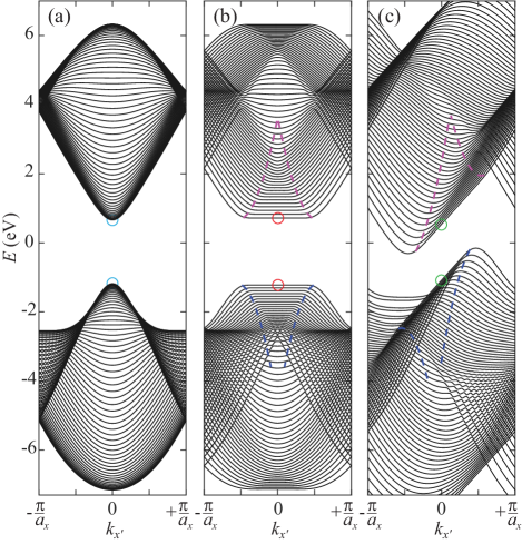
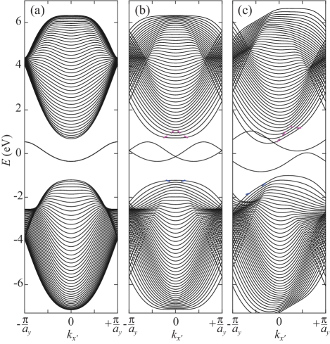
In Fig. 2 we show the band structures of AC nanoribbons: (a) in the absence of fields, (b) with applied magnetic field only, and (c) with both and turned on. In the absence of fields these nanoribbons are insulating, grujic16 and host a series of parabolic bands, which are effectively ”sampled” from the band structure of bulk phosphorene, as might be inferred from Fig. 2(a). When the magnetic field is turned on LLs are formed and flat-bands appear, as shown in Fig. 2(b). Quasiclassically, for states away from the edges the magnetic field enforces closed elliptical cyclotron orbits. These states in turn quantize into LLs and form the flat parts of the bands displayed in Fig. 2(b). Note that these segments get narrower at higher energies and lower magnetic fields; the reason being that the cyclotron radius enlarges, and therefore fewer orbits are uninterrupted by the edges.
As we discussed in the theory part, due to the large effective mass in the transversal ZZ direction confinement is strong, and LLs might be found almost as soon as is turned on. Therefore, a large number of LLs is supported by nanoribbons with AC edges. Dashed magenta and blue curves denote theoretically calculated edges of the flat-bands in the conduction and valence band, respectively. There is good agreement between these edges and our numerical results. One of the reasons for certain small differences is explained in Sec. II, and is related to the flexible condition for these edges, given in Eq. (36). The other reasons are finite width of the ribbon and interband coupling, zhou15 due to which the spacing between LLs decreases as we move from the top (bottom) of the valence (conduction) band. Therefore, are overestimated and slopes of the theoretically calculated edges are higher than the actual ones. Furthermore, we must bear in mind that the continuum approximation is valid in a relatively narrow range of momenta around the -point. Consequently, the discrepancy between the analytical and numerical results is larger for the AC ribbon.
When an electric field is applied the flat bands become linearly dependent on and appear as tilted. As predicted by theory, due to the linear term the bandgap switches to an indirect one, as soon as the in-plane electric field is applied. For the value of the electric field the band-gap closes, as might be observed from Fig. 2(c). Furthermore, shifts of these linear segments in momentum space seem to be almost equal for the conduction and valence band. Earlier, we analyzed the spectral shift with respect to the effective masses and found that . In the case of AC ribbons , where and , thus the spectral shifts have similar values for electrons and holes. We note that only for AC ribbons the shift is slightly larger for electrons than for holes. For all the other ribbons discussed in the paper, the mass-dependent part of the shift for the holes is approximately 1.5-3 times larger than for the electrons. Therefore, we expect that for ribbons other than AC, the holes are much more sensitive to the in-plane field than the electrons.
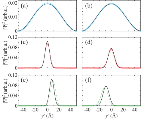
In Fig. 3 we show the real-space probability density of the states at the top (bottom) of the valance (conduction) band for . The states are marked with correspondingly colored circles in Fig. 2. Numerical results are compared to the analytical solutions. In order to compare probability densities found by the tight-binding model to those determined by means of the continuum approximation, we divide the probability for occupying a certain state by the distance between the adjacent atoms in each sublattice that is for AC and for all the other. When magnetic and electric fields are not present, confinement along transversal direction is as in an infinite potential well. Wavefunctions that are obtained numerically (denoted by open circles in Fig. 3) are compared to the theoretical expression
displayed by solid lines in Figs. 3(a) and (b), for the hole and the electron, respectively. We found that the wavefunction is spread along the ribbons with similar distribution for both, the electron and the hole, as predicted by the theoretical expression. According to expression (31) for the case when both magnetic and electric fields are applied, the ground state wavefunction at reads
| (40) |
When only the magnetic field is present we found excellent agreement between our numerical results and the theoretically predicted Gaussian function from our simplified model. Namely, almost perfect bell-shaped functions are formed in the middle of the ribbon, as may be inferred from Figs. 3(c) and (d) for the hole and electron, respectively. Good agreement is also found in the presence of electric field as shown in Figs. 3(d) and (e). The wavefunctions remain Gaussian-like but shift toward upper (lower) edge for the hole (electron).
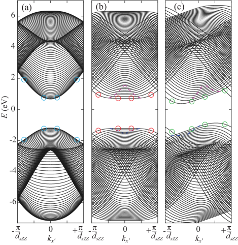
Next, we display the evolution of the band structure of sZZ nanoribbons in magnetic and electric fields in Fig. 4. In the absence of the fields, similarly for AC, these ribbons are insulating, as inferred from Fig. 4(a). When sufficiently large is applied, LLs are formed in the middle of the FBZ, i.e. the parabolic bands evolve, and start featuring dispersionless segments as we observed earlier in Fig. 4(b). By inspection of Fig. 4(b) we note that there is a smaller number of flat segments that are somewhat narrower than in the case of the AC ribbon with approximately the same width.
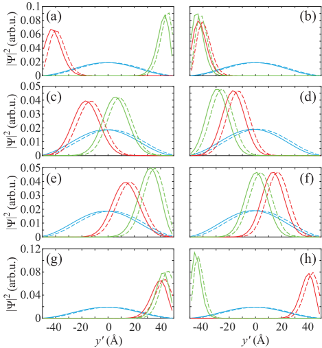
In order to elucidate these effects, in Fig. 5 we plot the real-space probability density of the ground states marked with correspondingly colored circles in Fig. 4, where solid and dashed curves depict on opposite sublattices. Both sublattices exhibit the same functional variation of , with a slight lateral offset, which is a general property, independent of the applied fields. The left (right) panel column corresponds to the valence (conduction) band, while the first, second, third and fourth row in the panel correspond to , , , and , respectively. In the absence of fields the ground electron and hole states fully extend across the ribbon width, regardless of the , as might be observed from the light blue curves in Figs. 5(a-h). For nonzero energy increases as described by , while confinement along ribbon width remains unchanged. The probability density of the ground states corresponding to the dispersionless segments in the valence (conduction) band are shown by the red curves in Figs. 5(c-f). We infer that these probability densities have almost unchangeable Gaussian shape for any in the flat-band range, as can be concluded by comparing the red curves in Figs. 5(c) and (e), for the valence band, as well as from Figs. 5(d) and (f), for the conduction band.
Next, we analyze effects of applied transverse electric field. By comparing the green curves in Figs. 5(b-g) to the red ones we found that the states are almost the same as in the case when only the magnetic field is applied. As expected, calculated wavefunctions in linear segments of the spectrum shown in Fig. 4(c) have the shape that is almost identical to the corresponding eigenfunctions in the flat-bands. However, these states are shifted along the ribbon width due to the electric field. For negative values of the longitudinal momenta where the dispersion is linear (see linear segments limited by dashed blue line in Fig. 4(c)), the hole wavefunction is localized around the center of the ribbon. Note that the valence band ground state at is not in the linear region, as shown in Fig. 4(c). In fact, since linear segments are much more shifted in the valence than in the conduction band, as displayed in Fig. 4(c). Therefore, the probability density displayed in Fig. 5(e) interferes with the upper ribbon edge, and differs from the bell-shaped function shown in Fig. 5(c).
However, the most intriguing behavior occurs near the left zone edge, where crossing is found for the hole ground state. The crossing involves the states localized at the opposite edges of the ribbon (see Fig. 4(c)). Therefore, the localization of the hole ground state can be abruptly changed by the electric field, as shown in Fig. 5(a). The same effect occurs in the conduction band, but near the upper edge of the FBZ (see Fig. 4(c)). Due to the crossing the electron localization switches to the opposite edge, as shown by the green curves in Fig. 5(h). Additionally, the position of the crossings can be tuned by magnetic field.
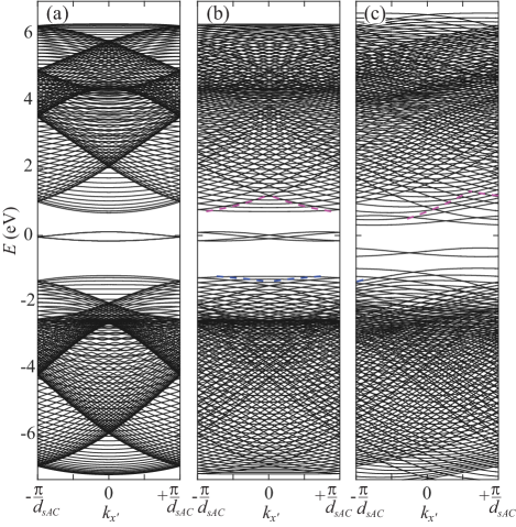
The band structures of zigzag nanoribbons are shown in Fig. 6. As discussed in the theoretical part, the interband coupling has a smaller influence on the motion along the -X direction and the dispersion is almost perfectly parabolic in most of the bands (see Fig. 6(a)). Since ZZ ribbons have weakest confinement in transversal direction even when a high is applied, only a few LLs evolve (see small regions encircled by dashed lines in Fig. 6(b)). When the electric field is applied, bands become immediately tilted, and newly formed linear bands are shifted. By comparing these shifts in the conduction and valence bands in Fig. 6(c), we realize that the hole is much more sensitive to the electric field, which is supported by the fact that the ratio for ZZ nanoribbons is the highest out of all considered ribbons.
In Fig. 7, we show the band structure of skewed armchair nanoribbons. Note that there are less flat segments in the spectrum of Fig. 7(b) corresponding to LLs forming around the middle of the ribbon than in the case of AC and sZZ ribbons. Also, these segments are much narrower, which can be explained by having in mind that the width of FBZ for sAC is 1.5-3 times narrower than for the other ribbon types. Since linear segments are much more shifted in the valence than in the conduction band, and dashed blue line delimiting linear bands starts at the band edge, as shown in Fig. 7(c).
Finally, we investigate the behavior of edge states. These states do not undergo Landau quantization, as can be seen in Fig. 6(b) and Fig. 7(b), which is a consequence of their exponential localization near the edges.grujic16 Instead, each QFB is effectively shifted along the axis, but in opposite directions. This behavior was absent in the case of edge states in zigzag graphene ribbons, since the corresponding bands were not fully detached from the bulk bands,ezawa14 as is the case with edge states in phosphorene nanoribbons.
In Fig. 8 we take a closer look at QFBs in (a) and (b) under a range of magnetic field values. In the absence of magnetic field, the bands are degenerate for both, ZZ and sAC, as depicted by solid blue curves in Fig. 8. It is clear that the QFBs get progressively shifted in opposite directions with increasing magnetic field (see red dashed lines in Fig. 8). An explanation for this behavior is very similar to the one given in Ref. [grujic15, ]; exponentially localized states ”sample” the vector potential only in a small area where it is effectively constant, and therefore the effect of magnetic fields amounts only to a phase shift. Additionally, the two QFB states are localized at opposite edges (at , for a ribbon of width ), where the local vector potential has different signs, which explains the opposite shifts.
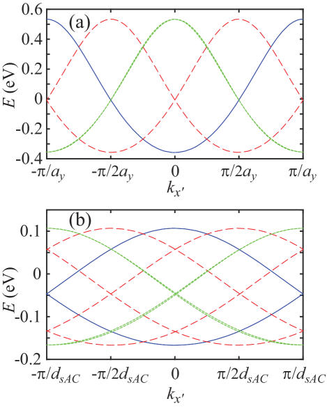
A quantitative description can be obtained by employing the principle of minimal coupling . In other words, the bands get shifted left and right by , depending on which edge they are localized at. We have confirmed that this is indeed a very good approximation for smaller fields. This also suggests that when , where is the unit cell length, QFBs get completely ”out of phase”, so that maxima and minima interchange places (see green dotted curves in Fig. 8). This critical magnetic field is then given as
| (41) |
which in fact means that the magnetic flux through the unit cell () is equal to one flux quantum ().
The exact expressions for the critical magnetic field in ZZ and sAC ribbons reads
| (42) | |||
| (43) |
respectively. Here, is the area of plaquet projection into the plane. The green dotted curves in Fig. 8 show the band structure at . However, these two bands are not degenerate and thus not exactly in opposition with respect to the solid blue curves. There are two reasons for this, both having to do with the fact that edge states have some finite spread towards the ribbon center. On the one hand, this means that the edge states effectively experience somewhat smaller ribbon widths (thus increasing true ). On the other hand, for larger magnetic fields the vector potential has a stronger spatial variation, so that the simple picture of phase shifts (assuming relatively constant in the narrow space occupied by the edge state) gradually losses validity.
IV Summary and Conclusions
In summary, we derived a new Hamiltonian to describe the electronic structure of phosphorene nanoribbons with arbitrary edges in transverse electric and perpendicular magnetic fields. We found that when a magnetic field is turned on the states of positive and negative momenta split to the opposite sides of the nanoribbon. An analytical expression for the minimal magnetic field when the bands become flat is obtained. The boundaries of these flat segments in momentum space are also described by analytical functions. We show that both the minimal field and the extension of the flat bands depend on the type of nanoribbon edge. Furthermore, when magnetic field increases, the Landau levels spectrum emerges first in an AC nanoribbon and last in the ZZ nanoribbon of equal width. Thus, the transversal confinement of electrons is found to be weakest in the ZZ nanoribbons and strongest in the AC nanoribbons. Moreover, an application of in-plane electric field causes the band gap to decrease and turns the previously flat segments into ranges of linear variation of the energy spectra in momentum space. We found that the electric field gives rise to shifts of crossings toward the center of the phosphorene Brillouin zone. For all ribbon types we found good agreement between the numerical results obtained by means of the tight binding and the results derived from an analytical model. Finally, the analytical expression for the critical magnetic when the edge states are localized at opposite edges acquire counter phases is derived for the cases of ZZ and sAC nanoribbons.
Acknowledgements.
This work was supported by the Serbian Ministry of Education, Science and Technological Development, and the Flemish Science Foundation (FWO-Vl).References
- (1) W. Lu, H. Nan, J. Hong, Y. Chen, C. Zhu, Z. Liang, X. Ma, Z. Ni, and C. Jin, Nano Research 7, 853 (2014).
- (2) H. Liu, A. T. Neal, Z. Zhu, Z. Luo, X. Xu, D. Tománek, and P. D. Ye, ACS Nano 8, 4033 (2014).
- (3) A. N. Rudenko, S. Yuan, and M. I. Katsnelson, Phys. Rev. B 92, 085419 (2015); A. N. Rudenko, S. Yuan, and M. I. Katsnelson, Phys. Rev. B 93, 199906(E) (2016).
- (4) R. Fei, A. Faghaninia, R. Soklaski, J.-A. Yan, C. Lo, and L. Yang, Nano Lett. 14, 6393 (2014).
- (5) Y. Aierken, D. Çakir, C. Sevik, and F. M. Peeters, Phys. Rev. B 92, 081408 (2015).
- (6) J. Qiao, X. Kong, Z.-X. Hu, F. Yang, and W. Ji, Nat. Commun. 5, 4475 (2014).
- (7) A. Favron, E. Gaufrès, F. Fossard, A.-L. P.-L’Heureux, N. Y-W. Tang, P.L. Lévesque, A. Loiseau, R. Leonelli, S. Francoeur and R. Martel, Nature Materials 14, 826 (2015).
- (8) Y. Cao, A. Mishchenko, G. L. Yu, E. Khestanova, A. P. Rooney, E. Prestat, A. V. Kretinin, P. Blake, M. B. Shalom, C. Woods, J. Chapman, G. Balakrishnan, I. V. Grigorieva, K. S. Novoselov, B. A. Piot, M. Potemski, K. Watanabe, T. Taniguchi, S. J. Haigh, A. K. Geim, and R. V. Gorbachev, Nano Lett. 15, 4914 (2015).
- (9) L. Li, G. J. Ye, V. Tran, R. Fei, G. Chen, H. Wang, J. Wang, K. Watanabe, T. Taniguchi, L. Yang, X. H. Chen, and Y. Zhang, Nature Nanotech. 10, 608 (2015).
- (10) X. Chen, Y. Wu, Z. Wu, Y. Han, S. Xu, L. Wang, W. Ye, T. Han, Y. He, Y. Cai, and N. Wang, Nat. Commun. 6, 7702 (2015).
- (11) A. S. Rodin, A. Carvalho, and A. H. Castro Neto, Phys. Rev. Lett. 112, 176801 (2014).
- (12) D. Çakir, H. Sahin, and F. M. Peeters, Phys. Rev. B 90, 205421 (2014).
- (13) M. M. Grujić, M. Ezawa, M. Ž. Tadić, and F. M. Peeters, Phys. Rev. B 93, 245413 (2016).
- (14) M. Ezawa, New. J. Phys. 16, 115004 (2014).
- (15) E. Taghizadeh Sisakht, M. H. Zare, and F. Fazileh, Phys. Rev. B 91, 085409 (2015).
- (16) X. Y. Zhou, R. Zhang, J. P. Sun, Y. L. Zou, D. Zhang, W. K. Lou, F. Cheng, G. H. Zhou, F. Zhai and Kai Chang, Sci. Rep. 5, 12295 (2015).
- (17) J. M. Pereira Jr. and M. I. Katsnelson, Phys. Rev. B 92, 075437 (2015).
- (18) B. Ostahie and A. Aldea, Phys. Rev. B 93, 075408 (2016).
- (19) L. C. Lew Yan Voon, A. Lopez-Bezanilla, J. Wang, Y. Zhang, M. Willatzen, New J. Phys. 17, 025004 (2015).
- (20) A. N. Rudenko and M. I. Katsnelson, Phys. Rev. B 89, 201408(R) (2014).
- (21) R. Winkler, Spin-orbit Coupling Effects in Two-Dimensional Electron and Hole Systems (Springer, Berlin 2003), pp. 164-166.
- (22) D.B. Topalović, V.V. Arsoski, S. Pavlović, N.A. Čukarić, M.Ž. Tadić, and F. M. Peeters, Commun. Theor. Phys. 65, 105 (2016).
- (23) D. J. P. de Sousa, L. V. de Castro, D. R. da Costa, and J. M. Pereira, Jr., Phys. Rev. B 94, 235415 (2016).
- (24) M. M. Grujić, M. Ž. Tadić, and F. M. Peeters, Phys. Rev. B 91, 245432 (2015).