In-gap features in superconducting - interfaces observed by tunneling spectroscopy
Abstract
We identified quasiparticle states at well-defined energies inside the superconducting gap of the electron system at the - interface using tunneling spectroscopy. The states are found only in a number of samples and depend upon the thermal-cycling history of the samples. The states consist of a peak at zero energy and other peaks at finite energies, symmetrically placed around zero energy. These peaks disappear, together with the superconducting gap, with increasing temperature and magnetic field. We discuss the likelihood of various physical mechanisms that are known to cause in-gap states in superconductors and conclude that none of these mechanisms can easily explain the results. The conceivable scenarios are the formation of Majorana bound states, Andreev bound states, or the presence of an odd-frequency spin triplet component in the superconducting order parameter.
I Introduction
Superconductors are characterized by the opening of a gap in the quasiparticle spectrum at the Fermi energy. The presence of states inside this gap indicates physics beyond conventional superconducting behavior and is, therefore, an exciting topic in science Hall et al. (1960); Rowell and McMillan (1966); Altshuler and Aronov (1979); Buchholtz and Zwicknagl (1981); Blonder et al. (1982); Alff et al. (1998); Kashiwaya et al. (1995); Kashiwaya and Tanaka (2000); Löfwander (2001); Deutscher (2005); SanGiorgio et al. (2008); Linder et al. (2010); Boden et al. (2011); Di Bernardo et al. (2015); Kitaev (2001); Fu and Kane (2008); Alicea (2012); Mourik et al. (2012); Beenakker (2013); Yu (1965); Shiba (1968); Rusinov (1969); Zittartz and Müller-Hartmann (1970); Kirtley and Tafuri (2007). There are different mechanisms that can cause a finite spectral density inside the superconducting gap. For example, for nodal superconductors, only a part of the Fermi surface is gapped, resulting in a smooth variation of the density of quasi-particle states as a function of energy inside the gap. In some cases, however, a peak in the spectral density is present at zero energy, or multiple peaks are present at finite energies. These peaks can be caused by, for example, Andreev bound states at interfaces between unconventional superconductors and normal metals Buchholtz and Zwicknagl (1981); Blonder et al. (1982); Alff et al. (1998); Kashiwaya et al. (1995); Kashiwaya and Tanaka (2000); Löfwander (2001); Deutscher (2005), an odd-frequency spin triplet component of the superconducting order parameter SanGiorgio et al. (2008); Linder et al. (2010); Boden et al. (2011); Di Bernardo et al. (2015), the solid-state analog of Majorana fermions Kitaev (2001); Fu and Kane (2008); Alicea (2012); Mourik et al. (2012); Beenakker (2013), and by bound states due to the presence of magnetic impurities Yu (1965); Shiba (1968); Rusinov (1969); Zittartz and Müller-Hartmann (1970). Zero bias anomalies also frequently appear in tunneling studies on high-temperature cuprate superconductors Kirtley and Tafuri (2007).The study of the in-gap states gives crucial information about the pairing symmetry of a superconductor. Here we report the presence of quasiparticle states inside the superconducting gap of the two-dimensional - interface superconductor.
At the interface of the two insulators and , a conducting two-dimensional electron system (2DES) with fascinating properties exists Ohtomo and Hwang (2004). In contrast to the more conventional 2DESs, which exist, e.g., at semiconductor heterointerfaces where the electrons are dilute and behave like a free electron gas, the conduction electrons at the - interface stem from local Ti 3d orbitals and exhibit unusual and novel properties. Due to correlations, the 2DES is often referred to as a two-dimensional electron liquid (2DEL) Breitschaft et al. (2010). To name only a few of these properties, the interface is gate-tunable Thiel et al. (2006) and exhibits superconductivity Reyren et al. (2007), which is also gate-tunable Caviglia et al. (2008). In addition, it is reported to be a host to a large number of other interesting phenomena, such as (gate-tunable) Rashba spin-orbit coupling Caviglia et al. (2010); Ben Shalom et al. (2010); Zhong et al. (2013) and the coexistence of superconductivity and magnetism Li et al. (2011); Bert et al. (2011). More aspects of the --interface 2DEL can be found in several review articles Hwang et al. (2012); Gariglio et al. (2016); Boschker and Mannhart (2017).
Recently, we performed tunneling measurements on - interfaces, allowing us to measure the superconducting gap, map the corresponding phase diagram Richter et al. (2013); Fillis-Tsirakis et al. (2016), and to identify electron-phonon coupling as a likely origin of the superconductivity Boschker et al. (2015). Almost all - tunneling samples investigated exhibit superconducting gap spectra with the expected BCS density of states consisting of a full gap and coherence peaks. In some cases, however, we observed spectra which exhibit distinct peaks inside the superconducting gap. The in-gap features appear and disappear non-deterministically upon different thermal cycles and gate-voltage sweeps. In this manuscript, we describe the structure and occurrence of these states and discuss the most likely scenarios of their origin.
II In-gap states
We give an overview over a selection of various in-gap states that can be observed in superconducting tunnel junctions and briefly explain their origins and properties. These states are summarized in Table II.
| Name | Properties |
| Origin | |
| Kondo resonance Kondo (1964) | Resonance effects observable as peaks in conductivity. Zero-bias peak splits in a finite magnetic field. Side-peak separation varies linearly with external magnetic field. Does not require superconductivity |
| Resonance at magnetic impurities located inside the conducting host. | |
| Anderson-Appelbaum statesAnderson (1966); Appelbaum (1966, 1967) | Similar to Kondo resonance (see above) |
| Exchange interaction between tunneling electrons and magnetic impurities located inside the tunnel barrier. | |
| Impurity states | Decrease of conductivity at zero bias (barrier states) Giaever and Zeller (1968) Increase of conductivity at zero bias (surface states) Samokhin and Walker (2001). In-gap states are particle-hole asymmetric. |
| Tunneling via intermediate impurity states in barrier or surface. | |
| Josephson junction characteristics | Gap of size . Cooper-pair tunneling DC Josephson current at zero bias. Peaks inside the larger gap at the gap difference . |
| Tunneling from to . | |
| Multiband SuperconductivityBinnig et al. (1980) | Two gaps inside one another. Two pairs of coherence peaks. |
| SC pairing in multiple bands. | |
| Caroli-de Gennes-Matricon states Caroli et al. (1964) | States below the gap energy. Bound states which are localized at the core of vortices. Comparable to Andreev Bound states (see below). |
| Andreev reflection at a vortex core. | |
| Yu-Shiba-Rusinov states Yu (1965); Shiba (1968); Rusinov (1969) | Paired peaks symmetric around zero energy. States are localized at the impurity sites. Peak positions move with varying magnetic field Zittartz and Müller-Hartmann (1970). |
| Bound states due to magnetic impurities in SC. | |
| Majorana bound states Kitaev (2001); Fu and Kane (2008) | Zero-energy bound state for well-separated Majoranas. Paired states at finite energies for interacting Majoranas Nilsson et al. (2008); Beenakker (2013); Flensberg (2010). Located at defects at which the SC gap closes. Conductance peak height quantized in units of for specific situations. |
| Emergent states at the boundary of topological superconductors. | |
| Andreev Bound statesDeutscher (2005) | For non--wave NS junction: peak at zero energy. For SNS junction: peaks at finite energies, depending on the phase difference between the SCs. |
| Successive Andreev reflections at NS-interfaces. | |
| Odd-frequency spin triplet pairing | Peaks at zero or finite energies depending on layer thickness and disorder. SanGiorgio et al. (2008); Linder et al. (2010); Boden et al. (2011); Di Bernardo et al. (2015); Eschrig and Löfwander (2008) Two pairs of coherence peaks in density of states. |
| Induced -wave pairing at interfaces between SC and inhomogeneous ferromagnet. |
Kondo resonance
The Kondo effect Kondo (1964) introduces a resonance at magnetic impurities, e.g., in tunneling processes through quantum dots Goldhaber-Gordon et al. (1998). The resonance effect is observable as a peak in conductivity. The peak appears usually at zero voltage bias, but can also be generated at finite voltage bias Sellier et al. (2005). Kondo resonances do not require superconductivity and, therefore, the in-gap states which originate from this mechanism do not in general disappear upon a superconducting transition. In the presence of an external magnetic field, the zero-bias peak splits by an amount equal to the Zeeman energy of the magnetic field. The splitting of the side peaks varies linearly with magnetic field Costi (2000). With increasing temperature, there is a reduction and broadening of the Kondo resonance Hänke et al. (2005).
Anderson-Appelbaum states
In the early 1960s, a zero-bias anomaly was observed in tunneling experiments in - junctions Hall et al. (1960); Logan and Rowell (1964) and in tunnel junctions composed of normal metals separated by oxide barriers Wyatt (1964). It was found that the zero-bias conductance peak varies logarithmically with temperature and, thereafter, this zero-bias anomaly was also known, in the literature, as the logarithmic anomaly. Anderson Anderson (1966) and Appelbaum Appelbaum (1966, 1967) showed that magnetic impurities located inside the tunneling barrier close to the electrodes can participate in an exchange interaction with the tunneling electrons, resulting in the zero-bias anomaly. The characteristics of these states are similar to those generated by the Kondo resonance.
Barrier and surface impurities
In tunnel junctions with a thick barrier, in which the probability for direct tunneling from one electrode to the other is small, impurity states enclosed in the barrier provide an alternative pathway for tunneling. In this case, electrons can tunnel via an intermediate state localized on the impurity state. Due to the finite capacitance of the particle, a minimum charging energy is required to add an electron to it. Such junctions show, therefore, a suppression in conductance around zero voltage bias Giaever and Zeller (1968). Localized states due to imperfections of the surface of a superconductor may facilitate bound states at low energy, causing peaks in the conductance around zero voltage bias Samokhin and Walker (2001).
Superconductor-insulator-superconductor (SIS) tunneling
The tunnel spectra observed in junctions of two superconductors separated by an insulating barrier show gaps of , where and are the gaps in the spectra of the two superconductors. At zero bias, a DC Cooper-pair current is observable, which depends on the relative phase of the two superconductors according to the first Josephson effect Josephson (1962); Anderson and Rowell (1963). At finite temperatures, a tunneling current flows at bias voltage equal to .
Multiband superconductivity
If two bands of a material participate in superconductivity, tunneling spectra can reveal a double gap structure with two sets of coherence peaks corresponding to the two separate pairing strengths. The coherence peaks of the band with smaller gap width will appear inside the gap of the band with larger pairing strength Binnig et al. (1980). In contrast to SIS-tunneling, the double gap of a multiband superconductor does not show a Josephson-current peak at zero bias.
Caroli-de Gennes-Matricon states
The electron system in the core of an Abrikosov vortex in a type-II superconductor can host localized fermionic bound states which are populated at energies smaller than the superconducting gap energy Caroli et al. (1964). The origin of this effect can be regarded as a specific form of Andreev reflection (see below), since a vortex core is a normal metal confined in a superconductor.
Yu-Shiba-Rusinov states
Based on Abrikosov-Gorkov theory Abrikosov and Gorkov (1961), Yu Yu (1965), Shiba Shiba (1968) and Rusinov Rusinov (1969) showed that magnetic impurities can facilitate bound states inside the superconducting gap. Tunneling measurements revealing such states were performed early Woolf and Reif (1965), and it was possible to resolve the contribution of individual impurity atoms on a Nb surface by scanning tunneling spectroscopy Yazdani et al. (1997); Salkola et al. (1997); Flatté and Byers (1997). Yu-Shiba-Rusinov (YSR) states always appear in pairs symmetrically around zero energy and move to higher energy with increasing magnetic field Zittartz and Müller-Hartmann (1970). For a review on impurity states in superconductors, see, e.g., Ref. [Balatsky et al., 2006].
Majorana bound states
Majorana fermions are particles which are their own antiparticles. While it is not yet clear whether elementary Majorana particles exist, there is growing evidence that collective states with Majorana-like properties can be created in solid-state systems Mourik et al. (2012); Nadj-Perge et al. (2014). Superconductors are the primary candidate to host such Majorana states, since Bogoliubov quasiparticles, the elementary excitations of a superconductor, are particle-hole symmetric and can indeed be described using Majorana’s original equations Chamon et al. (2010). Since a pair of Majoranas constitutes a Dirac fermion, the challenge is to create unpaired or spatially separated Majoranas. The two most common proposals to achieve this goal are either to combine a superconductor with a material with strong spin-orbit coupling (e.g. a topological insulator) Fu and Kane (2008); Mourik et al. (2012); Das et al. (2012) or to create a ferromagnetic chain at the surface of a superconductor Kitaev (2001); Nadj-Perge et al. (2014). In these cases, topological superconductivity is induced and isolated Majorana zero modes emerge at the edges of one-dimensional sample structures. If the two Majorana pair partners are well-separated, Majorana Bound States (MBS) are observed at zero energy, where superconducting quasiparticles are electron-hole symmetric. However, if the wavefunctions of the two pair partners overlap, a level splitting to finite energies can occur Beenakker (2013); Nilsson et al. (2008); Flensberg (2010). In the limit of zero temperature and ballistic conductance, the height of the zero-bias peak generated by MBS is quantized in units of . Reviews of the research on MBS in solid-state and other systems can be found e.g. in Refs. [Beenakker, 2013; Leijnse and Flensberg, 2012; Elliott and Franz, 2015].
Andreev bound states
Andreev reflections can facilitate bound states at zero energy in normal metal–superconductor (NS) junctions if the pairing symmetry of the superconductor is non s-wave Buchholtz and Zwicknagl (1981); Blonder et al. (1982); Alff et al. (1998); Deutscher (2005); Löfwander (2001); Kashiwaya et al. (1995); Kashiwaya and Tanaka (2000). Andreev bound states (ABS) also appear in SNS junctions, irrespective of the pairing symmetry de Gennes and Saint-James (1963); Tomasch (1965); Rowell and McMillan (1966); McMillan and Anderson (1966). It has been reported that ABS can also be generated at a SC-vacuum interface without any normal metal Hu (1994); Carrington et al. (2001). The ABS in SNS-junctions is located at zero bias if there is a phase difference of between the two superconductors. For other phase differences, it consists of two peaks at finite energies Blonder et al. (1982); Kashiwaya and Tanaka (2000). The peak height of these bound states may exceed the normal-state conductance. A zero-bias peak generated by an Andreev bound state is expected to split upon the application of magnetic field Fogelström et al. (1997). Andreev processes require sufficiently good conductance between the superconductor and the normal metal, usually a NS-contact without insulating barrier.
Odd-frequency spin triplet pairing
At superconductor–ferromagnet (SF) interfaces, a long-range proximity effect can induce odd-frequency superconductivity in the ferromagnet if magnetic disorder is present Eschrig and Löfwander (2008). This proximity-coupled superconductivity exhibits an odd-frequency, s-wave, spin-triplet component of the superconducting order parameter which generates in-gap peaks in tunnel spectra. The peaks appear at either finite or zero energy, depending on the relative thicknesses of the ferromagnetic and superconducting layers and on the magnetic disorder of the magnetic layerSanGiorgio et al. (2008); Linder et al. (2010); Boden et al. (2011); Di Bernardo et al. (2015).
Having discussed a number of effects which can cause states inside the superconducting gap in tunnel spectra, we now turn to the description of our experimental observations.
III Experiments
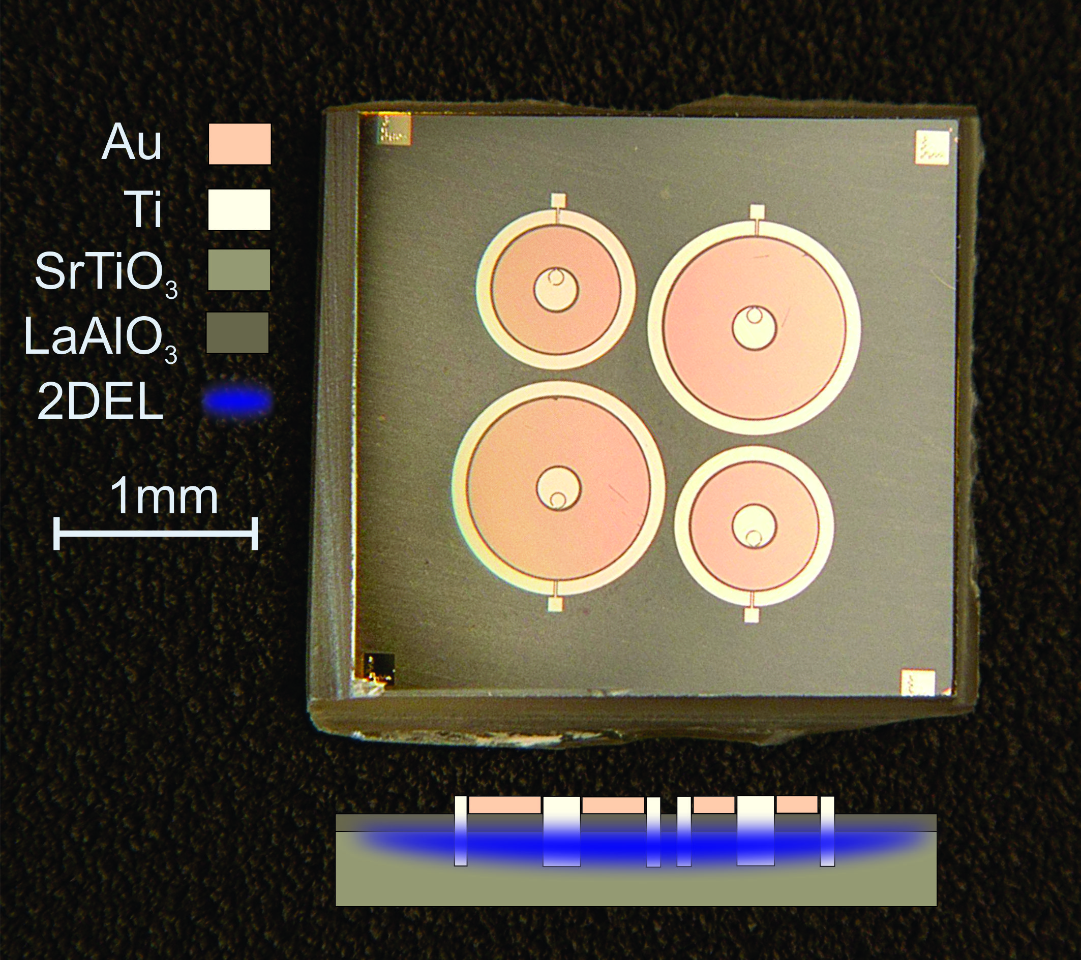
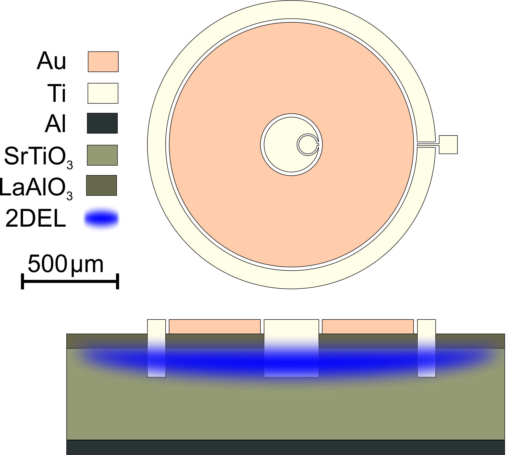
Our sample design, shown in Fig. 1, comprises a gold top electrode for tunneling measurements and titanium contacts to the - interface 2DEL for in-plane measurements. The outer titanium electrode is grounded during measurement and acts as shielding. The surface area of the gold electrode equals . This large size was chosen to yield a sizable tunneling current with sufficient energy resolution to resolve the -gap. The layer of 4 unit cells serves a dual purpose. It acts both as the generator of the conducting interface and as the tunneling barrier. The samples were glued with silver paste to an aluminum bottom electrode prior to the measurements, which allows us to tune the carrier density of the sample using the high- substrate. Descriptions of these samples have already been published in Richter et al. (2013) and their suitability to measure both the superconducting gap and the phonon peaks in inelastic tunneling Boschker et al. (2015) has been demonstrated.
The layer was grown by pulsed laser deposition (PLD) onto -terminated substrates with a fluence of at an oxygen pressure of . Growth was monitored using reflectivity high-energy electron diffraction (RHEED). Clear oscillations of the RHEED intensity indicated layer-by-layer deposition. Samples were subsequently annealed at oxygen pressure for one hour at and another hour at to ensure oxygen stoichiometry. A gold top layer was deposited in situ to avoid adsorbates on the surface. Devices were structured on the sample surface by photolithography. Then, the gold tunneling electrode was defined by etching with KI+I solution and electrodes to the 2DEL were created by ion milling with subsequent electron beam evaporation of Ti.
Tunneling measurements were performed in 4-point configuration using a Keithley 6430 Femtoamp Sourcemeter as current source and a Keithley 2001 or Keithley 2812 nanovolt meter. The polarity was such that a positive bias corresponds to electrons tunneling from the 2DEL into the gold electrode.
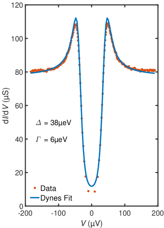
The shape of the superconducting gap observed in the tunneling spectra of - -interfaces follows the prediction for a standard s-wave BCS superconductor taking into account finite quasiparticle lifetime Dynes et al. (1978). However, in some samples and in some measurement runs, we observed distinct in-gap features inside the superconducting gap. These features are observable regardless of the sweep direction or sweep rate of the measurement. The in-gap features appear or disappear between different measurement runs, i.e. after a thermal cycle to room temperature: On sample A, in the first measurement run, standard tunneling spectra were observed on both of the devices which had been bonded (Fig. 2). After a thermal cycle to room temperature, both devices showed in-gap features such as shown in Fig. 3 (a) and (b). In a number of subsequent warming and cooling cycles, in-gap features of varying strength were observed in this sample (Fig. 3 (c)). On sample B, in the first measurement run the in-gap features shown in Fig. 3 (d) were observed after saturating the sample with charge carriers at high positive backgate voltage and then returning to zero backgate. The in-gap features were not observed in subsequent measurement runs on sample B. It is not clear why only specific samples show these anomalies and others do not.
IV Results
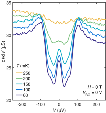
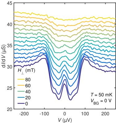
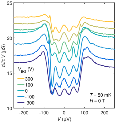
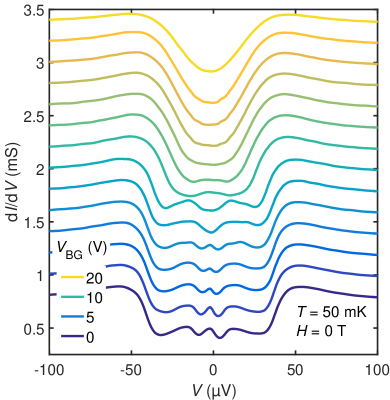
The in-gap structures are shown in Fig. 3 for two different samples grown in two different PLD systems. Fig. 3 (a) shows tunnel spectra of sample A as a function of temperature, Fig. 3 (b) shows spectra of sample A as a function of magnetic field, Fig. 3 (c) shows spectra of sample A from a different measurement run as a function of back-gate voltage and Fig. 3 (d) shows spectra from sample B as a function of back-gate voltage. The in-gap-features observed in Fig. 3 (a) and (b) consist of a strong peak at zero bias and two smaller peaks, one at either side of the gap. Additionally, the width of the gap is increased compared to the standard spectra with the smaller peaks appearing at voltage values comparable to those of the coherence peaks in the standard spectra. The in-gap features disappear at the same temperature and field scales as the superconducting gap itself, i.e. it is neither possible to observe the features without the gap, nor the gap without the features. Both the application of field and temperature suppress the gap and the features, but do not destroy them. Temperature was increased to and field to , after which the features reappeared when returning to base temperature and zero field. The intrinsic charge carrier density of sample A was so high that the 2DEL could not be depleted completely with the gate voltages accessible in our experiment. Only minor changes of the in-gap states were observed for -300 300 V (Fig. 3(c)).
In contrast to sample A, the spectra of sample B depend strongly on the applied gate voltage. For 10 V, no in-gap states were observed. For 10 V, first a single zero bias peak is present, then for decreasing gradually more peaks appear. At first sight, the tunneling spectra observed in Fig. 3 (c) and (d) appear to be quantitatively different from those observed in Fig. 3 (a) and (b). However, their similarity becomes obvious when a different distribution of spectral weight between the central and the side peaks is taken into account.
To gain quantitative information on the properties of the observed in-gap-peaks, we performed the fitting routine illustrated in Fig. 4: For each curve, a lifetime-broadened BCS fit (Dynes fit) was adjusted to the part of the superconducting gap without peaks to create a reference curve corresponding to a standard - gap. Since spectral weight is shifted from the coherence peaks into the in-gap peaks, the coherence peaks are not described well by this fit. The Dynes curve was subtracted from the data points to obtain the deviation from standard superconducting behavior. Three Gaussians were fitted to this subtracted peak to obtain the position, size and full width at half maximum (FWHM) of the central zero-bias peak and the separation of the side peaks.
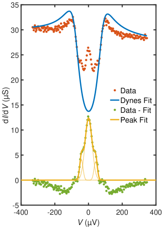
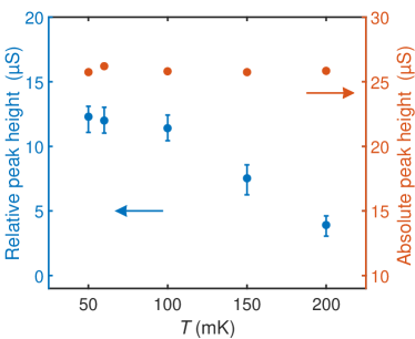
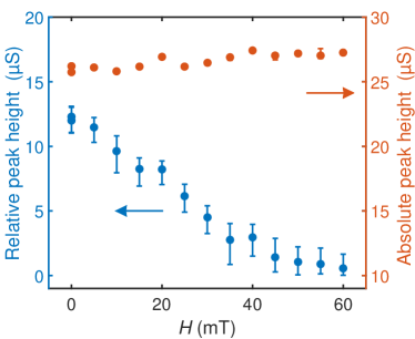
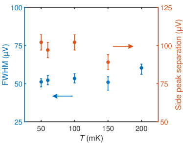
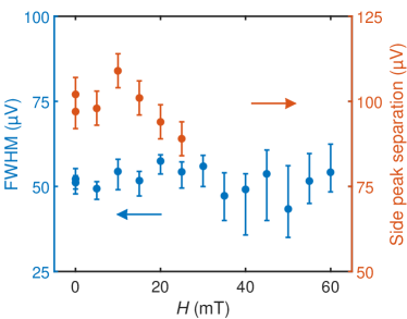
Results of this analysis are shown in Fig. 5: The size of the subtracted peak decreases monotonically with increasing temperature or magnetic field and disappears at the same values of temperature and field at which the gap closes. On the other hand, the absolute height of the peak remains almost constant over the entire measurement range close to the value corresponding to outside the gap. Also both the FWHM of the central peak and the separation of the outer peaks is independent of temperature and magnetic field. Since only few data points are available for the Dynes fits, the error bars given in Fig. 5 are based on the fit uncertainty: For the optimal fit, the sum of residuals, i.e. of the weighted difference squares between data and fit curve, is minimal. Error bars denote results from fits at the border of the confidence interval, for which the sum of residuals is twice as large as for the optimal fit.
V Discussion
Origin of the in-gap states
We now discuss the applicability of the phenomena described in Section II to our experimental data. Since we always observe either three peaks or no peaks at all, we conjecture that all peaks are caused by the same mechanism. Therefore, we concentrate our discussion on those mechanisms which can account for all observed peaks.
Kondo resonance
A strong peak at zero bias can be caused by a Kondo resonance. However, the observed side peaks cannot be easily explained in a Kondo framework. Also, a zero-bias-anomaly caused by Kondo scattering is expected to split with increasing magnetic field, which we do not observe. Finally, the zero-bias-peak in the measurements disappears at the same temperature and field as the superconducting gap, hinting at an intimate connection between the peak and superconductivity. We therefore conclude that Kondo scattering is unlikely to be the origin of the observed in-gap states.
Anderson-Appelbaum states
Similarly to Kondo resonances, Anderson-Appelbaum states are not connected to superconductivity. Also, the side-peak separation does not vary linearly with external magnetic field, as expected for these states. We therefore do not consider them as likely candidates for the origin of the observed in-gap states.
Barrier and surface impurities
Both the barrier and surface impurity models account only for features at zero bias but cannot explain the side peaks at finite voltage. We therefore conclude that they are unlikely to be the origin of the observed in-gap states.
Superconductor-insulator-superconductor (SIS) tunneling
Both the zero bias current and the broadening of the gap to approximately twice the value of standard - (cf. Fig. 2) can clearly be seen in the data from sample A. Thus the tunnel characteristics observed here strongly resemble that of a hypothetical SIS junction, with the side peaks representing the coherence peaks of the inner gap. However, there is only one superconducting electrode in the tunnel junction. It is implausible that the superconducting - interface induces superconductivity in the gold top electrode through the insulating tunneling barrier. We therefore conclude that SIS tunneling is an unlikely explanation of the observed in-gap states.
Multiband superconductivity
The side peaks observed in our tunneling spectra are explicable as the coherence peaks of a second superconducting band. However, the strong peak at zero bias cannot be explained in this framework. Also, the coherence peaks of a second gap should move closer together as the gap closes with increasing magnetic field or temperature, which is not observed. Therefore, we conclude that multiband superconductivity is not a likely explanation of our observations.
Caroli-de Gennes-Matricon states
In our experiment, the peak at zero bias becomes weaker with increasing magnetic field, i.e., with an increasing number of vortices. Thus it shows the opposite behavior of that expected for CdGM-states. We therefore believe that the CdGM-mechanism is not the origin of the observed in-gap states.
Yu-Shiba-Rusinov states
YSR states can cause multiple peaks inside the gap of superconductors with magnetic impurities. However, YSR states always appear in pairs around zero, therefore the single peak at zero bias shown in Fig. 3 would be explicable only as a smeared pair of two YSR states. Such a smeared peak should broaden as the two constituent peaks move apart with increasing magnetic field, which is not observed. Also the two peaks on either side remain at the same position independent of magnetic field, in contrast to the outward movement expected for YSR states. The range of magnetic fields accessible in our experiment is limited because the critical magnetic field of our - samples is small. We therefore have performed simulations to assure that the movement of the peak positions should indeed be observable on the magnetic field scales investigated, if the peaks were due to YSR states. Since we observe neither a broadening of the central peak nor a movement of the side peaks, we conclude that YSR states are most likely not the origin of the observed in-gap states.
Majorana bound states
The zero bias peak observed on sample A is of almost constant height as expected for a MBS. The fixed position of the peak at zero bias is consistent with the hypothesis of MBS, with the peaks at finite voltage bias possibly indicating Majoranas with overlapping wavefunctions Nilsson et al. (2008); Beenakker (2013); Flensberg (2010). The - -interface has been suggested as a candidate host for MBS Mohanta and Taraphder (2014), since it comprises the basic ingredients required for topological superconductivity viz. -wave superconductivity, Rashba spin-orbit coupling and magnetism. The appearance of Majorana modes usually requires specific configurations of the 2DES, e.g., magnetic oxygen vacancies arranged in a linear chain which is quite unlikely to be readily available at the inhomogenous interface. However, scanning superconducting quantum interference device (SQUID) measurements provide evidence for the existence of one-dimensional conducting channels at the domain boundaries of substrate SrTiO3 Kalisky et al. (2013). The possibility of MBS as the origin of the in-gap states cannot be ruled out.
Andreev bound states
ABS can generate conductance peaks at zero bias as well as at finite energy, consistent with our observations. However, a zero-bias conductance peak caused by an ABS is expected to split upon increasing the magnetic field, which we do not observe. Andreev bound states usually occur at junctions of superconductors with metals which have sufficiently high conductivity, whereas in our samples, gold electrode and superconductor are separated by an insulating layer. However, the NS contact can be situated within the 2DES, either as an in-plane combination of normal and superconducting islands or as separate normal and superconducting layers. The application of gate voltage changes the carrier density and hence the superconducting volume fraction, changing the number of the ABS.
Odd-frequency spin-triplet pairing
Odd-frequency spin-triplet pairing can account for both the zero bias peak and the side peaks. It requires an inhomogeneous magnetization at the interface, which in some regions of the sample generates zero-bias peaks and peaks at finite bias in other regions. Since the area of our tunnel junctions is larger than the domain size, the peaks from different regions are observed together in our spectra. However, the gap size for singlet pairing and triplet pairing is likely to differ and therefore an averaging over triplet and singlet regions should show a double gap with two pairs of coherence peaks, unless the condensate is always either completely singlet or completely triplet. Magnetism has been observed to coexist with superconductivity in - Li et al. (2011); Bert et al. (2011) and it has been shown to be rather superparamagnetic than truly ferromagnetic in nature Li et al. (2011). Therefore, the difference between the superparamagnetic domains could generate an inhomogeneous magnetization if the variation of magnetization between domains is strong enough.
Origin of the dependence on thermal cycling
Finally, we speculate on some scenarios that could explain the fact that the in-gap states are only observed in a small fraction of samples and that they depend on thermal cycling. A tentative explanation for the appearance and disappearance of sub-gap states may lie in the domain structure of the substrate: as the crystal structure changes from cubic to tetragonal when the crystal is cooled below 105 K, a domain structure forms, which is randomly different in each measurement run. If we assume the in-gap states to depend on a specific domain configuration, then this scenario can also explain why the in-gap features sometimes disappear irreversibly when sweeping the gate voltage, because the gate voltage influences the domain structure Honig et al. (2013). Another possible explanation is that the in-gap states depend on a specific configuration of defects in the samples, for example oxygen vacancies. Oxygen vacancies form magnetic centersPavlenko et al. (2012) and could thereby influence the superconductivity. Finally, we mention that the back-gate voltage also affects the thickness of the superconducting sheet, with increased up to a factor of three in the overdoped region Gariglio et al. (2016).
VI Conclusions
Using tunneling spectroscopy on the two-dimensional superconductor, we have observed in-gap features in spectra of several superconducting - tunnel devices. The features appear and disappear non-deterministically between different warming and cooling cycles. The in-gap states were found not to move with either temperature or magnetic field, yet to change under the application of back-gate voltage. The real challenge is to disentangle the true origin of these in-gap states with the limited information available at the buried interfaces. None of the known mechanisms that can cause in-gap states easily explains the results. Conceivable scenarios involve Majorana bound states, Andreev bound states, or the presence of an odd-frequency spin-triplet component in the superconducting order parameter caused by an inhomogeneous ferromagnetic state in the electron system.
Acknowledgements.
We thank Y. Fominov, C. Renner, and A. Santander-Syro for enlightening discussions.References
- Hall et al. (1960) R. N. Hall, J. H. Racette, and H. Ehrenreich, Phys. Rev. Lett. 4 (1960).
- Rowell and McMillan (1966) J. M. Rowell and W. L. McMillan, Phys. Rev. Lett. 16, 453 (1966).
- Altshuler and Aronov (1979) B. L. Altshuler and A. G. Aronov, Solid State Commun. 30, 115 (1979).
- Buchholtz and Zwicknagl (1981) L. J. Buchholtz and G. Zwicknagl, Phys. Rev. B 23, 5788 (1981).
- Blonder et al. (1982) G. E. Blonder, M. Tinkham, and T. M. Klapwijk, Phys. Rev. B 25, 4515 (1982).
- Alff et al. (1998) L. Alff, S. Kleefisch, and U. Schoop, Eur. Phys. J. B 438, 423 (1998).
- Kashiwaya et al. (1995) S. Kashiwaya, Y. Tanaka, M. Koyanagi, and K. Kajimura, Jpn. J. Appl. Phys. 34 (1995).
- Kashiwaya and Tanaka (2000) S. Kashiwaya and Y. Tanaka, Reports Prog. Phys. (2000).
- Löfwander (2001) T. Löfwander, Supercond. Sci. Technol. Sci. Technol. (2001).
- Deutscher (2005) G. Deutscher, Rev. Mod. Phys. 77, 109 (2005).
- SanGiorgio et al. (2008) P. SanGiorgio, S. Reymond, M. R. Beasley, J. H. Kwon, and K. Char, Phys. Rev. Lett. 100, 237002 (2008).
- Linder et al. (2010) J. Linder, A. Sudbø, T. Yokoyama, R. Grein, and M. Eschrig, Phys. Rev. B 81, 214504 (2010).
- Boden et al. (2011) K. M. Boden, W. P. Pratt, and N. O. Birge, Phys. Rev. B 84, 020510 (2011).
- Di Bernardo et al. (2015) A. Di Bernardo, S. Diesch, Y. Gu, J. Linder, G. Divitini, C. Ducati, E. Scheer, M. G. Blamire, and J. W. A. Robinson, Nat. Commun. 6, 8053 (2015).
- Kitaev (2001) A. Y. Kitaev, Physics-Uspekhi 171 (2001).
- Fu and Kane (2008) L. Fu and C. L. Kane, Phys. Rev. Lett. 100, 096407 (2008).
- Alicea (2012) J. Alicea, Reports Prog. Phys. 75, 076501 (2012).
- Mourik et al. (2012) V. Mourik, K. Zuo, S. M. Frolov, S. R. Plissard, E. P. A. M. Bakkers, and L. P. Kouwenhoven, Science 336, 1003 (2012).
- Beenakker (2013) C. Beenakker, Annu. Rev. Condens. Matter Phys. 4, 113 (2013).
- Yu (1965) L. Yu, Acta Phys. Sin. (1965).
- Shiba (1968) H. Shiba, Prog. Theor. Phys. 40 (1968).
- Rusinov (1969) A. I. Rusinov, Sov. Phys. JETP 29 (1969).
- Zittartz and Müller-Hartmann (1970) J. Zittartz and E. Müller-Hartmann, Zeitschrift für Phys. 232, 11 (1970).
- Kirtley and Tafuri (2007) J. R. Kirtley and F. Tafuri, in Handbook of High-Temperature Superconductivity, edited by J. R. Schrieffer and J. S. Brooks (Springer, 2007) Chap. 2.
- Ohtomo and Hwang (2004) A. Ohtomo and H. Hwang, Nature 427, 423 (2004).
- Breitschaft et al. (2010) M. Breitschaft, V. Tinkl, N. Pavlenko, S. Paetel, C. Richter, J. R. Kirtley, Y. C. Liao, G. Hammerl, V. Eyert, T. Kopp, and J. Mannhart, Phys. Rev. B 81, 153414 (2010).
- Thiel et al. (2006) S. Thiel, G. Hammerl, A. Schmehl, C. W. Schneider, and J. Mannhart, Science 313, 1942 (2006).
- Reyren et al. (2007) N. Reyren, S. Thiel, A. Caviglia, L. Fitting Kourkoutis, G. Hammerl, C. Richter, C. W. Schneider, T. Kopp, A. S. Ruetschie, D. Jaccard, M. Gabay, D. A. Muller, J. M. Triscone, and J. Mannhart, Science 1196 (2007), 10.1126/science.1146006.
- Caviglia et al. (2008) A. D. Caviglia, S. Gariglio, N. Reyren, D. Jaccard, T. Schneider, M. Gabay, S. Thiel, G. Hammerl, J. Mannhart, and J. Triscone, Nature 456 (2008), 10.1038/nature07576.
- Caviglia et al. (2010) A. D. Caviglia, M. Gabay, S. Gariglio, N. Reyren, C. Cancellieri, and J.-M. Triscone, Phys. Rev. Lett. 104, 126803 (2010).
- Ben Shalom et al. (2010) M. Ben Shalom, M. Sachs, D. Rakhmilevitch, A. Palevski, and Y. Dagan, Phys. Rev. Lett. 104, 126802 (2010).
- Zhong et al. (2013) Z. Zhong, A. Tóth, and K. Held, Phys. Rev. B 87, 161102 (2013).
- Li et al. (2011) L. Li, C. Richter, J. Mannhart, and R. C. Ashoori, Nat. Phys. 7, 762 (2011).
- Bert et al. (2011) J. A. Bert, B. Kalisky, C. Bell, M. Kim, Y. Hikita, H. Y. Hwang, and K. A. Moler, Nat. Phys. 7, 767 (2011).
- Hwang et al. (2012) H. Y. Hwang, Y. Iwasa, M. Kawasaki, B. Keimer, N. Nagaosa, and Y. Tokura, Nat. Mater. 11, 103 (2012).
- Gariglio et al. (2016) S. Gariglio, M. Gabay, and J.-M. Triscone, APL Mater. 4, 060701 (2016).
- Boschker and Mannhart (2017) H. Boschker and J. Mannhart, Annu. Rev. Condens. Matter Phys. 8, annurev (2017).
- Richter et al. (2013) C. Richter, H. Boschker, W. Dietsche, R. Jany, F. Loder, L. F. Kourkoutis, D. A. Muller, J. R. Kirtley, C. W. Schneider, and J. Mannhart, Nature 502, 528 (2013).
- Fillis-Tsirakis et al. (2016) E. Fillis-Tsirakis, C. Richter, J. Mannhart, and H. Boschker, New J. Phys. 18, 013046 (2016).
- Boschker et al. (2015) H. Boschker, C. Richter, E. Fillis-Tsirakis, C. W. Schneider, and J. Mannhart, Sci. Rep. 5, 12309 (2015).
- Kondo (1964) J. Kondo, Prog. Theor. Phys. 32, 37 (1964).
- Anderson (1966) P. W. Anderson, Phys. Rev. Lett. 17, 5 (1966).
- Appelbaum (1966) J. Appelbaum, Phys. Rev. Lett. 17 (1966).
- Appelbaum (1967) J. A. Appelbaum, Phys. Rev. 154 (1967).
- Giaever and Zeller (1968) I. Giaever and H. R. Zeller, Phys. Rev. Lett. 20, 24 (1968).
- Samokhin and Walker (2001) K. V. Samokhin and M. B. Walker, Phys. Rev. B 64, 172506 (2001).
- Binnig et al. (1980) G. Binnig, A. Baratoff, H. E. Hoenig, and J. G. Bednorz, Phys. Rev. Lett. 45, 1352 (1980).
- Caroli et al. (1964) C. Caroli, P. G. de Gennes, and J. Matricon, Phys. Lett. 9, 307 (1964).
- Nilsson et al. (2008) J. Nilsson, A. R. Akhmerov, and C. W. J. Beenakker, Phys. Rev. Lett. 101, 120403 (2008).
- Flensberg (2010) K. Flensberg, Phys. Rev. B 82, 180516 (2010).
- Eschrig and Löfwander (2008) M. Eschrig and T. Löfwander, Nat. Phys. 4, 138 (2008).
- Goldhaber-Gordon et al. (1998) D. Goldhaber-Gordon, H. Shtrikman, D. Mahalu, D. Abusch-Magder, U. Meirav, and M. A. Kastner, Nature 391, 1996 (1998).
- Sellier et al. (2005) G. Sellier, T. Kopp, J. Kroha, and Y. S. Barash, Phys. Rev. B 72, 174502 (2005).
- Costi (2000) T. Costi, Phys. Rev. Lett. 85, 0 (2000).
- Hänke et al. (2005) T. Hänke, M. Bode, S. Krause, L. Berbil-Bautista, and R. Wiesendanger, Phys. Rev. B 72, 085453 (2005).
- Logan and Rowell (1964) R. Logan and J. Rowell, Phys. Rev. Lett. 13 (1964).
- Wyatt (1964) A. Wyatt, Phys. Rev. Lett. 13, 401 (1964).
- Josephson (1962) B. Josephson, Phys. Lett. 1, 7 (1962).
- Anderson and Rowell (1963) P. Anderson and J. Rowell, Phys. Rev. Lett. , 230 (1963).
- Abrikosov and Gorkov (1961) A. A. Abrikosov and L. P. Gorkov, Sov. Phys. - JETP 39, 866 (1961).
- Woolf and Reif (1965) M. A. Woolf and F. Reif, Phys. Rev. 137 (1965).
- Yazdani et al. (1997) A. Yazdani, B. A. Jones, C. P. Lutz, M. F. Crommie, and D. M. Eigler, Science 275 (1997).
- Salkola et al. (1997) M. I. Salkola, A. V. Balatsky, and J. R. Schrieffer, Phys. Rev. B 55, 12648 (1997).
- Flatté and Byers (1997) M. E. Flatté and J. M. Byers, Phys. Rev. B 56, 11231 (1997).
- Balatsky et al. (2006) A. V. Balatsky, I. Vekhter, and J.-X. Zhu, Rev. Mod. Phys. 78, 373 (2006).
- Nadj-Perge et al. (2014) S. Nadj-Perge, I. K. Drozdov, J. Li, H. Chen, S. Jeon, J. Seo, A. H. MacDonald, B. A. Bernevig, and A. Yazdani, Science 346 (2014).
- Chamon et al. (2010) C. Chamon, R. Jackiw, Y. Nishida, S.-Y. Pi, and L. Santos, Phys. Rev. B 81, 224515 (2010).
- Das et al. (2012) A. Das, Y. Ronen, Y. Most, Y. Oreg, M. Heiblum, and H. Shtrikman, Nat. Phys. 8, 887 (2012).
- Leijnse and Flensberg (2012) M. Leijnse and K. Flensberg, Semicond. Sci. Technol. 27, 124003 (2012).
- Elliott and Franz (2015) S. R. Elliott and M. Franz, Rev. Mod. Phys. 87, 137 (2015).
- de Gennes and Saint-James (1963) P. G. de Gennes and D. Saint-James, Phys. Lett. 4, 4 (1963).
- Tomasch (1965) W. Tomasch, Phys. Rev. Lett. 1 (1965).
- McMillan and Anderson (1966) W. McMillan and P. Anderson, Phys. Rev. Lett. 16, 16 (1966).
- Hu (1994) C.-R. Hu, Phys. Rev. Lett. 72 (1994).
- Carrington et al. (2001) A. Carrington, F. Manzano, R. Prozorov, R. W. Giannetta, N. Kameda, and T. Tamegai, Phys. Rev. Lett. 86, 1074 (2001).
- Fogelström et al. (1997) M. Fogelström, D. Rainer, and J. A. Sauls, Phys. Rev. Lett. 79, 281 (1997).
- Dynes et al. (1978) R. C. Dynes, V. Narayanamurti, and J. P. Garno, Phys. Rev. Lett. 41, 1509 (1978).
- Mohanta and Taraphder (2014) N. Mohanta and A. Taraphder, EPL (Europhysics Lett. 108, 60001 (2014).
- Kalisky et al. (2013) B. Kalisky, E. M. Spanton, H. Noad, J. R. Kirtley, K. C. Nowack, C. Bell, H. K. Sato, M. Hosoda, Y. Xie, Y. Hikita, C. Woltmann, G. Pfanzelt, R. Jany, C. Richter, H. Y. Hwang, J. Mannhart, and K. A. Moler, Nat. Mater. 12, 1091 (2013).
- Honig et al. (2013) M. Honig, J. A. Sulpizio, J. Drori, A. Joshua, E. Zeldov, and S. Ilani, Nat. Mater. 12, 1112 (2013).
- Pavlenko et al. (2012) N. Pavlenko, T. Kopp, E. Y. Tsymbal, G. A. Sawatzky, and J. Mannhart, Phys. Rev. B 85, 020407 (2012).