Influence of image forces on the electron transport in ferroelectric tunnel junctions
Abstract
We study influence of image forces on conductance of ferroelectric tunnel junctions. We show that the influence of image forces is twofold: i) they enhance the electro-resistance effect due to polarization hysteresis in symmetric tunnel junctions at non-zero bias and ii) they produce the electro-resistance effect due to hysteresis of dielectric permittivity of ferroelectric barrier. We study dependence of ferroelectric tunnel junction conductance on temperature and show that image forces lead to strong conductance variation with temperature.
I Introduction
Recent progress in fabrication techniques allows creating nanometer scale ferroelectric (FE) films [Fong et al., 2004; Lichtensteiger et al., 2005; Tenne et al., 2006; Bune et al., 1998] and FE tunnel junctions (FTJ) where metallic leads are separated by tunnel barrier made of FE material [Tian et al., 2016; Crassous et al., 2010; Barrionuevo et al., 2014; Usui et al., 2014; Pantel et al., 2014; Hou et al., 2016]. The most promising and important property of FTJ is the electro-resistance (ER) effect meaning the dependence of the FTJ linear conductance on the polarization direction of the FE layer. The ER effect can be used for non-volatile memory applications [Garcia and Bibes, 2014; Kim et al., 2012; Boyn et al., 2014; Wang et al., 2014]. Several phenomena were considered to be responsible for ER effect in FTJ such as barrier thickness variation due to strain in FE [Zheng and Woo, 2009; Kohlstedt et al., 2005], variation of band structure of FE layer [Kohlstedt et al., 2005] and the appearance of surface charges at the FE/metal interfaces [Zhuravlev et al., 2005; Tsymbal and Kohlstedt, 2006]. It was demonstrated that the last mechanism is the strongest one leading to the giant ER (GER) effect up to 1000%. ER effect linear in FE polarization appears only in asymmetric FTJs with essentially different metallic leads or in metal/FE/semiconductor structures [Wen et al., 2013; Tsymbal and Gruverman, 2013].
In symmetric TJ with the leads made of the same metal the ER effect appears for non-linear conductance at finite bias. In this case the contribution to the conductance contains a combination of polarization and the bias voltage. The magnitude of the effect is not as high as GER in asymmetric FTJ, but may reach several tens of percent [Kohlstedt et al., 2005] which is comparable to magnetoresistance effect in magnetic tunnel junctions considered for memory application as well. While the ER effect in symmetric FTJ is not as high as in asymmetric junction, using of the same material for both electrode is an advantage for fabrication process.
The above mentioned mechanisms deform the potential barrier height, thickness and shape leading to the ER effect. There is however another mechanism modifying the barrier in TJ, namely the image forces acting on electron moving through the barrier. It is known that image forces reduce the barrier height and its thickness in TJ [Burstein and Lundqvist, 1969]. It is also known that the strength of image forces depends on the dielectric constant of the barrier. In FEs the dielectric constant depends on the external parameters such as the applied voltage, temperature and the direction of FE polarization (at non-zero bias). Thus, one can control image forces in FE barrier with external parameters in FTJ and therefore there is one more way to control the barrier parameters and the tunnelling probability. In the present paper we investigate the influence of the image forces on the conductance of the FTJ. We will show that image forces may also produce the ER effect at non-zero bias in symmetric and asymmetric FTJ. In strongly asymmetric junctions the image forces can be neglected while in symmetric TJ the presence of image forces is crucial.
Recently, the dependence of FTJ conductance on temperature was investigated in asymmetric FTJ [Zhao et al., 2015]. The effect was related to the variation of polarization (surface charges) with temperature. It exists only below the FE Curie point. Here we show that similar effect may occur due to the image forces. In FE the dielectric constant strongly varies with temperature leading to variations of image forces strength and thus to the temperature dependence of the FTJ conductance. Since the dielectric constant varies with temperature both below and above the FE Curie point the dependence of the FTJ conductance on temperature should appear in the whole temperature range.
Recently, the influence of image forces were considered and observed in hybrid systems consisting of FE and thin film of granular metal (GM). Image forces lead to strong dependence of granular film conductivity on temperature [Udalov et al., 2014a]. In a field effect transistor with granular channel and the FE placed between the channel and the gate electrode the image forces lead to the ER effect [Udalov et al., 2014b]. The dependence of the granular film conductivity on temperature in FE/GM system was observed in Refs. [Huth et al., 2014a, b]. It was demonstrated that image forces influence the strength of the Coulomb blockade effect and influence the conductivity of granular metals. In Refs. [Udalov et al., 2015a,Udalov et al., 2015b] it was theoretically shown that the image forces are responsible for coupling between FE substrate and magnetic granular film (magneto-electric effect).
It is important that typical FEs have a high dielectric constant (of order of 1000). Such FEs are not suitable for observation of image forces effects, since the strength of image forces is inversely proportional to the FE dielectric susceptibility. FEs with low dielectric constant are more suitable. There are a number of low dielectric constant FEs such as hafnium oxide family XHfO2 (where X can be Y, Co, Zr, Si) [Olsen et al., 2012; Park et al., 2014; Boscke et al., 2011], rare-earth manganites XMnO3 (where X is the rare-earth element) [Goto et al., 2004], colemanite [Fatuzzo, 1960], Li-doped ZnO [Wang et al., 2003], etc. There are also numerous organic FEs with low dielectric constant [Naber et al., 2010; Zhang and Xiong, 2012; Horiuchi and Tokura, 2008]. Most FTJ up to date were fabricated with BTO barrier having a very high dielectric constant. One can neglect image forces in this type of TJs. However, the low endurance and extremely complicated fabrication process restricted applications of oxide FEs so far. Organic FEs provide an alternative approach [Tian et al., 2016] with low cost processing and opportunities to fabricate flexible electronic devices. Such FEs are in the track of emerging field of organic electronics. Note that FTJ with organic FE were fabricated and showed significant TER effect recently [Tian et al., 2016]. Organic FEs mostly have a low dielectric constant and image forces should play a crucial role in FTJ with organic FEs. Another important point is that dielectric properties of FE materials weaken with decreasing of film thickness [Fridkin, 2006]. FEs with moderate dielectric constant may have a rather weak dielectric response as they embedded as few nm thick layer in FTJ.
II The model
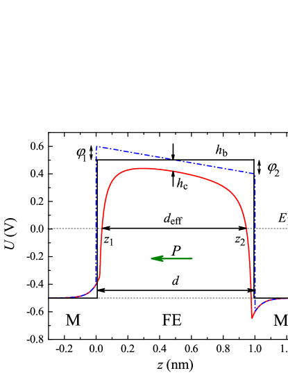
To study tunnelling currents in FTJ we use the following model. Consider a FTJ with FE barrier having polarization , dielectric constant and thickness (see Fig. 1). The polarization is assumed to be uniform across the barrier and directed perpendicular to the barrier surfaces. A voltage is applied to the FTJ. The leads of the FTJ are made of good metals with the Fermi momentum and , respectively. We assume that the Fermi energy of the leads is large enough such that the screening lengths in these metals are small, (). In this case one can use a simple picture of image forces to describe the correlation effects inside the insulating barrier. Following Refs. [Burstein and Lundqvist, 1969; Zhuravlev et al., 2005] we describe the barrier seen by transport (close to Fermi level) electrons measured in Volts as follows (region )
| (1) |
with
| (2) |
Here is the electron charge, is the vacuum dielectric constant, is the coordinate perpendicular to the layers surfaces; defines the barrier height above the Fermi level of the left lead (which is energy zero in our model) in the absence of FE polarization, image forces and external voltage. Potentials in Eq. (1) are due to formation of surface charges at the FE/metal interfaces. These charges occur due to polarization of the FE layer as well as due to screening of polarization by electrons in metallic leads. The potentials are found using Thomas-Fermi approximation with close circuit conditions (see Ref. [Zhuravlev et al., 2005]).
The third term in Eq. (1) describes the influence of the image forces. These forces appear due to the interaction of electron inside the barrier with image charges occurring in metallic leads. Calculating the image forces potential we consider metallic leads as ideal, neglecting corrections due to finite screening length. When calculating potentials the finite screening length is crucial and can not be neglected.
The last term in Eq. (1) describes the effect of the applied voltage.
In our model the Fermi energy of both metals is larger than potentials and (, is the electron mass). This means that potentials created by the FE polarization together with voltage do not produce the charge depleted layer inside the leads. This is in contrast to the case of FTJ having at least one lead with small Fermi energy considered in numerous papers. In such a FTJ the surface charges turn a metal lead with small Fermi level into an insulator in the vicinity of FE/metal interface leading to the increase of effective barrier width.
In our model the effective barrier thickness can be decreased due to image forces or in the situation when the potentials and exceed the barrier height (). This situation may easily occur if the barrier height is less than eV.
II.1 FE layer
We use the following model of FE layer: below the Curie point the spontaneous FE polarization is a function of applied voltage and has a hysteresis with the switching voltage and the saturation polarization . We use the following formula capturing these peculiarities of FE layer
| (3) |
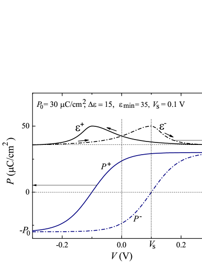
where “” and “” correspond to the upper and the lower hysteresis branch respectively, is the width of the transition region. For example, the polarization of HfZrO2 is shown in Fig. 3 and can be approximately described with the following parameters: C/cm2, V (with being measured in m), and . We use these values of and in all our calculations. The parameters were obtained by fitting the experimental curves of Ref. [Muller et al., 2012]. TbMnO3 which also have rather low dielectric constant can be described with the following parameters: C/cm2, V, [Lee et al., 2006].
We introduce the dependence of dielectric permittivity on applied voltage below the Curie temperature
| (4) |
This dependence captures the basic features of dielectric constant behavior as a function of electric field. The dielectric permittivity has two branches corresponding to two polarization states. In the vicinity of the switching bias the dielectric permittivity, has a peak. Note that sometimes in the literature the following function is used , where and are fitting parameters. There is no qualitative difference between this formula and Eq. (4) in the range of voltages we study. For higher voltages Eq. (4) gives a finite dielectric constant which is more correct than the zero given by . The second order phase transition theory gives diverging at , which is also not suitable for description of real systems.
Not much data are currently available on voltage dependencies of for FEs with low dielectric constants. For example, the dielectric constant of HfZrO2 can be described using the following parameters: , (see Fig. 2).
The dielectric constant of TbMnO3 has a much lower variation of dielectric constant, , [Lee et al., 2006]. Therefore HfZrO2 is better suited for checking our predictions.
Below we also study the temperature dependence of FTJ conductance using experimental data on . We model the temperature dependence of FE dielectric constant using the following formula
| (5) |
This function allows to capture all peculiarities of behavior, namely the finite height peak at (where is the FE Curie temperature), dependence aside the immediate vicinity of as well as asymmetry of curve with respect to the point . We keep the function continuous at the point .
II.2 Calculation of resistance
We assume that the FE barrier is thin enough and the electron transport occurs due to tunnelling. To calculate the electric current across the barrier we use Simmon’s formula [Simmons, 1963a, b]
| (6) |
where
| (7) |
the parameter and . The integration in Eq. (7) is performed over the region where which can differ from the region [] due to surface charges and image forces effects. The coordinates where are denoted as and and is the effective barrier thickness. The constant is of order of 1. Equation (6) is just the difference between currents created by electrons in left (the first term) and right (the second term) leads. Since the Fermi level in the right lead is biased by the applied voltage, the potential barrier seen by electrons in this lead is higher (lower) by for positive (negative) voltage. Therefore, the average potential in the second term of Eq. (6) is calculated with replaced by .
Below we find the TJ resistance and the conductance
| (8) |
We use the superscript “” (“-”) to describe conductance and resistance corresponding to the upper (lower) hysteresis branch of FE layer.
Also we introduce the conductance for TJ in the absence of image forces and the conductance which neglects the surface charges effect.
The ER effect due to both polarization and image forces is given by the ratio, . We use the subscripts or to denote the ER effect caused by the surface charges () or the image forces (), respectively. To calculate and we neglect the third and the second term in Eq. (1), respectively.
III Tunnelling barrier average height and thickness. Analytical estimates
In this section we compare the influence of image forces and surface charges on the average TJ barrier parameters.
III.1 General remarks
Since the dielectric constant at zero bias is the same for both branches (), the image forces do not lead to the dependence of the linear TJ resistance on the FE polarization state () even for asymmetric FTJ with . In contrast, the FE surface charges produce the ER effect in asymmetric FTJ even at zero bias, . At finite zero-bias both mechanisms lead to the ER effect.
First, we compare the influence of the image force mechanism and the surface charge mechanism for the case of symmetric TJ. Second, we discuss the case of asymmetric TJ.
III.2 Influence of the image forces
Image forces reduce both the barrier height and the thickness. The characteristic potential associated with image forces in TJ is given by the expression
| (9) |
This is the reduction of the initial potential barrier height (see Eq. (1)) at the symmetry point (, see Fig. 1) at zero bias. For and nm we have V. The ratio of and defines the effective barrier thickness as follows
| (10) |
One can see that the influence of the image forces on the height and the thickness increases with decreasing of FE dielectric constant and the barrier thickness. The barrier thickness reduction exceeds 10% only for even for the smallest feasible . Therefore we can always treat it as a small perturbation and approximate . In Sec. II.2 we introduced the average barrier height as follows, . We use this expression in our numerical calculations. For analytical consideration of the influence of image forces it is enough to use a simpler expression, , where integration is over the region [] and the term with is neglected. The tunnelling probability is defined by the product of potential barrier and its average height
| (11) |
Corrections due to the image forces are defined by the ratio . These estimates show that correction to the resistance due to image forces increases with decreasing of FE dielectric constant , but is independent of the barrier thickness since the common factor is compensated by in the factor . Decreasing the barrier height also increases the influence of the image forces.
III.3 Influence of FE surface charges
First we consider the symmetric case, , in which the potential is an odd function of and gives a zero contribution to the average potential, . The effect of surface charges appears only due to the fact that enters the tunnelling probability in a non-linear way. Therefore in the case of surface charges one should use the average potential calculated in Eq. (7) to estimate its influence. Here we assume that potentials are smaller than the Fermi energy and the surface charges do not change the barrier thickness. We have
| (12) |
For symmetric TJ we have . For small and () the above expression can be written as
| (13) |
The ratio defines the contribution of surface charges to the effective barrier height. One can see that the surface charges effect decreases faster with increasing of (as ) in comparison with the effect of image forces. It is also important that the last term in the brackets may change its sign.
We estimate for . For , C/cm2, nm and nm we find V. The potential can be increased with increasing thickness . Also, there are many materials with polarization larger than C/cm2. Thus, in contrast to the case of image forces the influence of surface charges can be made very strong. The influence of surface charges decreases with decreasing of polarization , and thickness . The dielectric permittivity enters this mechanism in the same way as in the mechanisms based on image forces. However, as we show below, the dependencies of and on are different. The influence of dielectric permittivity voltage dependence on the surface charges ER effect was studied in Ref. [Zhang et al., 2011]. The potential decreases with for , however this regime is difficult to reach for thickness of about 1 nm.
III.4 Comparing image forces and surface charge contributions to ER effect
The ER effect is defined by the change of the effective barrier height and thickness under the change of FE state (approximately ). For symmetric barrier the expression in the exponent is non-zero only for finite bias. The polarization switching leads to the change of dielectric constant (). The variation of the barrier due to the image forces is given by
| (14) |
where . The barrier variation due to the surface charges has the form
| (15) |
Comparing these expressions we can estimate the ratio of two mechanisms contributing to the ER effect (we use ). In this ratio is the difference of dielectric constants for positive and negative polarization, . If this ratio is larger than 1 then the image forces define the ER effect, otherwise the surface charges are more important. For example, for nm and % the image forces mechanism is more pronounced for C/cm2.
III.5 Asymmetric TJ
For asymmetric TJ the resistance at zero bias depends on the direction of polarization. This effect appears due to the surface charges of the FE layer in combination with asymmetric screening of these charges. Here we compare this ER effect at zero bias with ER at due to image forces.
For asymmetric TJ the average potential (neglecting image forces) is given by the expression, and the relative change of is given by . This expression does not take into account a variation of barrier thickness appearing for leads with Fermi energy smaller than . Comparing the expression with the relative barrier change due to image forces we can write the ratio . We can neglect the image forces in asymmetric TJ if this ratio is larger than 1. This is the case when BTO or PZT FE is used in asymmetric TJ made of Pt and LSMO metals. We note that to create the TJ with % one has to use the metals with Fermi level difference of about 40%, since .
IV Electro-resistance effect in FTJ
In this section we compare the ER effect for symmetric and asymmetric FTJ appearing due to image forces and due to surface charges. We discuss the behavior of the ER effect on system parameters such as barrier height and thickness, saturation polarization and dielectric constant. We calculate all curves using Eqs. (6), (7) and (8).
IV.1 Symmetric FTJ
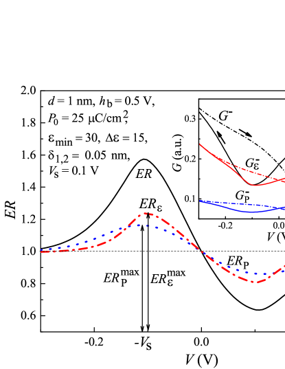
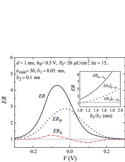
The inset in Fig. 3 shows the behavior of FTJ conductance for symmetric barrier as a function of applied bias. The curves have a hysteresis character originating from the hysteresis of polarization and the dielectric constant . For symmetric TJ with the conductance at zero bias is the same for both hysteresis branches. At non-zero bias the symmetry of the TJ is broken due to external field leading to difference in conductance for different hysteresis branches. The chosen parameters correspond to Hf0.5Zr0.5O2 FE material.
There are three pairs of curves in the inset in Fig. 3. Black lines show the conductance calculated by taking into account both the surface charge and the image forces effects. Blue lines show the conductance calculated neglecting the image forces, . The conductance has its minimum when polarization switching occurs ( for the upper branch and for the lower branch). The minimum can be understood as follows: Surface charges produce the electric field inside the barrier leading to the linear slope of the potential (see Fig. 1). The applied bias also creates the electric field inside the barrier. According to Eq. (12) the stronger the total field the lower the TJ resistance. Depending on the sign of polarization and voltage these two fields can enhance (co-directed) or counteract each other (counter-directed). Consider the positive bias (). For upper branch the fields are co-directed and the conductance grows (see Eq. (12)). For lower branch the fields are counter-directed decreasing the conductance. When the bias reaches the switching voltage the FE polarization changes its sign and both fields (due to bias and due to polarization) become co-directed for the lower branch. Further bias increase leads to the increase of the lower branch conductance.
Red lines in the inset in Fig. 3 are for conductance . If one moves left along the upper branch (decreasing voltage starting with large positive bias) the dielectric constant reaches its maximum value at negative bias (at ). The maximum dielectric constant weakens the image forces doing the barrier higher. Thus, the conductance decreases in the vicinity of for the upper branch ( for the lower branch). Thus, the change of conductance due to surface charges and image forces behaves similarly. However, the average (over the whole voltage region) conductance, , exceeds the average , meaning that image forces influence the conductance much stronger than the surface charges for given parameters.
Typical dependencies of ER effect on the applied voltage in symmetric FTJ are shown in Fig. 3. The black solid line shows the ER effect calculated by taking into account both the image forces and the surface charges (), the blue dotted line is for the ER effect calculated by taking into account only the surface charges (), the red dash-dotted line corresponds to the ER effect due to image forces (). The parameters for which the curves were calculated correspond to Hf0.5Zr0.5O2 FE. Due to the symmetry of the hysteresis loop in Eqs. (3) and (4) the ER effect obeys the relation . At zero bias the conductance does not depend on the FE state and the ER effect is absent (). At high voltage the FE state is the same for both branches and the ER effect is absent. The ER effect reaches its maximum value at switching voltage. We denote it for ER effect due to image forces, for ER effect due to the surface charges, and for ER effect including both mechanisms. One can see that for given parameters the image forces produce stronger ER effect than the surface charges. This is in agreement with our analytical estimates showing that image forces are important for 1 nm thick FTJ.
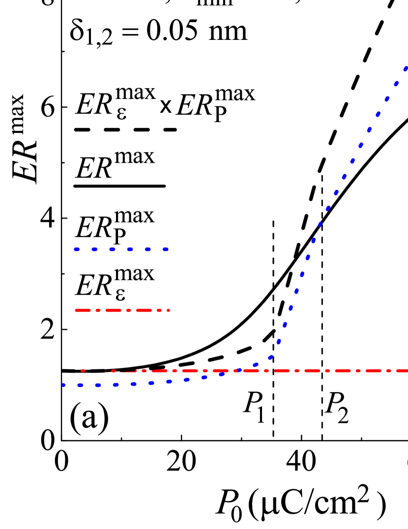
Figure 4 shows the dependence of the maximum value of the ER effect (, and ) on the parameters of FE barrier (saturation polarization , dielectric constant variation and and the barrier height ). First, consider the left panel in the figure. When calculating the dependencies on polarization (Fig. 4(a)) we fixed the switching voltage and the dielectric constant for the upper and the lower branch. The dotted line corresponds to the maximum ER effect due to surface charges. At zero this mechanism does not lead to the ER effect. The ER effect grows with increasing . The growth regime changes at points . For small polarization and the surface charges change the average barrier height according to Eq. (12). For the surface charges change the effective barrier thickness (this effect is absent in Eq. (12)). This leads to discontinuity of the derivative of . At the condition is satisfied for the lower polarization branch. At the same condition is fulfilled for the upper branch.
The red dash-dotted line shows the ER effect due to the image forces. It does not depend on the saturation polarization. Comparing and one can see that for small polarization the image forces effect, , exceeds the surface charge effect, . For large saturation polarization the situation is the opposite.
Interestingly that the total ER effect is not just a product of and shown with black dashed line. At low saturation polarization the total ER effect exceeds while at large polarization one has, .
Figure 4(b) shows the dependence of the maximum ER effect on the variation of dielectric constant (main graph) and on (inset). A variation of dielectric constant is the reason for ER effect due to image forces according to our analytical estimates, Eq. (14). Therefore, grows with increasing of reaching its maximum value when variation of dielectric constant becomes of the same order as the average dielectric constant (). Further increase of dielectric constant variation leads to the decrease of the ER effect. According to Eq. (14) the ER effect behaves as . The numerator of this expression grows with . But the denominator grows too due to the finite width of the transition region, . According to Eq. (4) increasing of leads to the increase of both and . Thus at a certain value the ER effect starts decreasing. Reducing the width of the transition region, , one can increase the ER effect due to the image forces.
In Fig. 4(b) the value of does not exceed several tens of percent. Generally, there is no restriction on the value of ER effect. One can expect the magnitude of the effect of order of for small width of the transition region . For and the magnitude of can be as high as 7 (the ER effect due to image forces is about 700%) if .
The contribution of surface charges simply decreases with increasing of . This effect is related to finite width of the transition region . At one has and for the upper branch. Therefore, only and enter . For we have and does not influence . For finite we have and it grows with increasing of leading to the decrease of the ER effect due to surface charges.
The inset in Fig. 4(b) shows the dependence of maximum ER effect on the minimum dielectric permittivity for variation of the dielectric constant scaled with (). The maximum value of ER effect due to the image forces decays as , in agreement with Eq. (14). The ER effect due to surface charges decays much faster and even changes sign at the point . For the potentials are mostly governed by dependence and for variation of with becomes more important. Figure 3 shows the case with . In the opposite limit the dependence of the ER effect due to surface charges on voltage, , is a reflected version of Fig. 3 with respect to the point .
Absence of the ER effect at can be understood using Eq. (13). We calculate at . At this point the upper branch has zero polarization and the lower branch has the polarization . The conductance for the upper branch is defined by the quantity . The potential profile has an upward tilt due to the bias. The conductance for the lower branch depends on . The electric field and the field due to the surface charges inside the barrier are counter-directed. For small absolute value of voltage the potential profile has the downward tilt larger than the tilt of the potential profile of the upper branch. Increasing the bias absolute value we decrease the tilt of for lower branch and increase the tilt of for upper branch. The point (see inset in Fig. 4(b)) is given by the equation . When this condition is satisfied the potential profiles for the upper and the lower branches have exactly the opposite tilt and the value of is the same for both branches.
The inset in Fig. 4(b) shows that the ER effect due to image forces exceeds the surface charges effect in a wide range of dielectric constants for symmetric FTJ.
Both contributions to the total ER effect and depend on the barrier height. These dependencies are shown in Fig. 4(c). One can see that increasing the barrier height increases the importance of image forces. For low barrier, exceeds , while for high barrier the situation is the opposite. This coincides with analytical estimates. Equation (14) shows that corrections due to image forces to the average barrier height multiplied by thickness behave as . The magnitude of behaves similarly. The effect of surface charges decays as according to Eq. (15). This difference in the behaviour appears due to the fact that image forces produce the correction even in average potential while the surface charges give the zero correction to the average potential. The surface charges contribute to the conductance only if one takes into account the fact that the tunnelling probability is a function of average of square root of the barrier.
Equation (13) shows that surface charges contribution grows with increasing of the screening length. Note that for large enough screening length, the approach used in the manuscript is not valid. The contribution due to the image forces does not depend on the screening length in our model for .
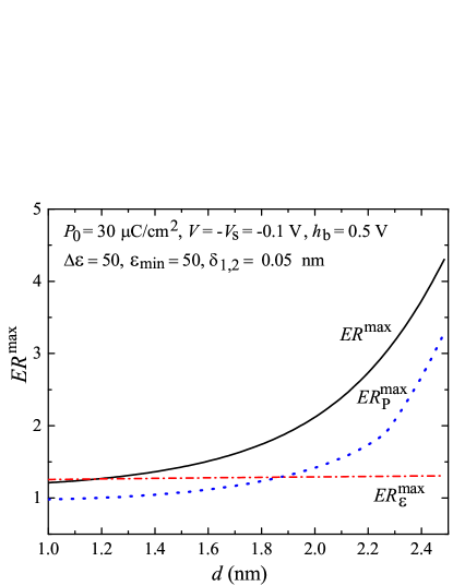
In the previous section we mentioned that the image forces contribution becomes less important with increasing of the barrier thickness. This is shown in Fig. 5. One can see that the value grows rapidly with thickness, while is almost independent of .
To summarize this section, we show that the contribution due to image forces to the ER effect exceeds the surface charge contribution for small barrier thickness and high barrier height, at small polarization and high variation of dielectric constant. Increasing the average dielectric constant increases the importance of image forces contribution reducing the contribution due to surface charges.
IV.2 Asymmetric FTJ
For asymmetric FTJ the surface charges produce the ER effect even at zero bias while image forces do not lead to the ER effect in this case (see Fig. 6). Therefore, comparison of ER effect at is not a correct way to proceed. Here we compare the ER effect due to image forces at () with the ER effect due to surface charges at zero bias voltage (see inset in Fig. 6). One can see that the effect due to surface charges grows rapidly with increasing the asymmetry and exceeds the ER effect due to image forces. Even 10% difference in the screening length produces the ER effect at zero bias of the same magnitude as the ER effect due to image forces at . Note however, that 10% difference in the screening length corresponds to 50% difference in the Fermi level of the material and corresponds to 16 times difference of the Fermi levels. Thus, the leads should be made out of essentially different materials to produce a strong ER effect at zero bias.
IV.3 Temperature dependence of conductance of FTJ
The important peculiarity of the image forces contribution to the conductance is related to the fact that it does not vanish above the ferroelectric Curie point while the surface charges are zero in this temperature region. The dielectric permittivity of FE strongly depends on temperature above (and below) . This leads to a strong dependence of the FTJ conductance on temperature above and below the phase transition point. Such a dependence above occurs only due to the image forces. Using Eq. (11) one can estimate the temperature coefficient of resistance for symmetric FTJ as follows
| (16) |
This quantity is independent of the barrier thickness and decays with increasing the barrier height and the average dielectric constant.
So far FTJ were made with only few FE materials: most FTJs have BTO FE with rather high dielectric constant ( 1000). The temperature dependence of conductance in symmetric FTJ with BTO due to image forces is very weak, see Eq. (16). In a recent paper, however the TCR of asymmetric FTJ with BTO was reported. The dependence of conductance on temperature appears due to surface charges produced by the FE layer. The dependence of on temperature occurs below the FE Curie point and the TCR of order 3.8% was reported in this system.

To observe a strong temperature dependence of TJ conductance due to image forces one needs to use FE with low dielectric constant. Recently, an organic ferroelectric P(VDF-TrFE) was used as a TJ barrier and the GER effect was demonstrated in this system. P(VDF-TrFE) has rather small dielectric constant depending on temperature in the vicinity of the Curie point C. Figure 7 shows the TCR for symmetric FTJ with P(VDF-TrFE) barrier. We fit the experimental data of Ref. [Bune et al., 1998] on P(VDF-TrFE) dielectric constant as a function of temperature, (see inset in Fig. 7) with Eq. (5). The magnitude of TCR reaches 3%. Note that P(VDF-TrFE) has rather small saturation polarization (C/cm2). Therefore, the main contribution to the TCR is produced by the image forces and surface charges can be neglected below . Above the temperature dependence of TJ conductance appears only due to image forces.
There are numerous organic FEs with low dielectric constant (, see review paper [Zhang and Xiong, 2012]). Usually these FEs have a very small saturation polarization (C/cm2). Such organic FEs can be promising candidates for TJ with high TCR. These FEs have the Curie temperature in a wide range from 50 K (TTF-BA) to a room temperature (Ca2Pb(CH3CH2COO)6). In some of these FEs the dielectric constant changes strongly (from 10 to 100) in a very narrow temperature range ( K) leading to large TCR of order of 50%/K (for example Ca2Ba(CH3CH2COO)6, see Fig. 8). Some of these FEs have a wide peak of dielectric constant around leading to moderate TCR in a wide temperature range.

V Conclusion
We studied influence of image forces on the ER effect and conductance temperature dependence in FTJs. Image forces inside the FTJ barrier reduce the average barrier height and strongly influence the TJ conductance. These forces produce the ER effect at non-zero bias. The effect appears due to dependence of the FE dielectric constant on the applied bias. For symmetrical FTJ (with identical metal electrodes) the ER effect due to image forces may exceed the ER effect due to surface charges at the FE/metal interfaces. The ER effect due to image forces increases with decreasing the barrier height and average barrier dielectric constant and almost independent of the barrier thickness. The importance of this mechanism (in comparison to the surface charges mechanism) grows with increasing of barrier height and decreasing of saturation polarization and barrier thickness. The magnitude of the effect for HfZrO2 FE reaches 50%.
For strongly asymmetric barrier the contribution of image forces to the ER effect is small in comparison to the effect of surface charges. The contribution of the image forces to the ER effect is visible only for TJ with metallic leads where difference of Fermi levels does not exceed 50%.
We studied temperature dependence of the FTJ conductance by taking into account the image forces. Above the FE Curie point the image forces is the only mechanism for dependence of the TJ conductance on temperature. Below both the surface charges and the image forces contribute to the temperature dependence of conductance. Large TCR can be achieved in FTJ with FE with low dielectric constant in the vicinity of the FE phase transition. We calculated the TCR for FTJ with P(VDF-TrFE) barriers. The peak value of TCR is about 3%/K which is comparable with TCR obtained in asymmetric FTJ with BTO barrier. According to our analysis the best materials for observing the strong temperature dependence of TJ conductance are organic FEs. These materials have a low dielectric constant with strong relative variation. For example, TJ with SrCa2Sr(CH3CH2COO)6(D) barrier leads to TCR up to 50% in the narrow temperature range.
VI Acknowledgements
This research was supported by NSF under Cooperative Agreement Award EEC-1160504, the U.S. Civilian Research and Development Foundation (CRDF Global) and NSF PREM Award. O.U. was supported by Russian Science Foundation (Grant 16-12-10340).
References
- Fong et al. (2004) D. D. Fong, G. B. Stephenson, S. K. Streiffer, J. A. Eastman, O. Auciello, P. H. Fuoss, and C. Thompson, Science 304, 1650 (2004).
- Lichtensteiger et al. (2005) C. Lichtensteiger, J.-M. Triscone, J. Junquera, and P. Ghosez, Phys. Rev. Lett. 94, 047603 (2005).
- Tenne et al. (2006) D. A. Tenne, A. Bruchhausen, N. D. Lanzillotti-Kimura, A. Fainstein, R. S. Katiyar, A. Cantarero, A. Soukiassian, V. Vaithyanathan, J. H. Haeni, W. Tian, D. G. Schlom, K. J. Choi, D. M. Kim, C. B. Eom, H. P. Sun, X. Q. Pan, Y. L. Li, L. Q. Chen, Q. X. Jia, S. M. Nakhmanson, K. M. Rabe, and X. X. Xi, Science 313, 1614 (2006).
- Bune et al. (1998) A. V. Bune, V. M. Fridkin, S. Ducharme, L. M. Blinov, S. P. Palto, A. V. Sorokin, S. G. Yudin, and A. Zlatkin, Nature 391, 874 (1998).
- Tian et al. (2016) B. Tian, J. Wang, S. Fusil, Y. Liu, X. Zhao, S. Sun, H. Shen, T. Lin, J. Sun, C. Duan, M. Bibes, A. Barthelemy, B. Dkhil, V. Garcia, X. Meng, and J. Chu, Nature Communications 7, 11502 (2016).
- Crassous et al. (2010) A. Crassous, V. Garcia, K. Bouzehouane, S. Fusil, A. H. G. Vlooswijk, G. Rispens, B. Noheda, M. Bibes, and A. Barthelemy, Appl. Phys. Lett. 96, 042901 (2010).
- Barrionuevo et al. (2014) D. Barrionuevo, L. Zhang, N. Ortega, A. Sokolov, A. Kumar, P. Misra, J. F. Scott, and R. S. Katiyar, Nanotechnology 25, 495203 (2014).
- Usui et al. (2014) S. Usui, T. Nakajima, Y. Hashizume, and S. Okamura, Appl. Phys. Lett. 105, 162911 (2014).
- Pantel et al. (2014) D. Pantel, H. Lu, S. Goetze, P. Werner, D. J. Kim, A. Gruverman, D. Hesse, and M. Alexe, Appl. Phys. Lett. 100, 232902 (2014).
- Hou et al. (2016) P. Hou, J. Wang, and X. Zhong, Euro. Phys. Lett. 115, 26003 (2016).
- Garcia and Bibes (2014) V. Garcia and M. Bibes, Nature Comm. 5, 4289 (2014).
- Kim et al. (2012) D. J. Kim, H. Lu, S. Ryu, C.-W. Bark, C.-B. Eom, E. Y. Tsymbal, , and A. Gruverman, Nano Lett. 512, 5697 (2012).
- Boyn et al. (2014) S. Boyn, S. Girod, V. Garcia, S. Fusil, S. Xavier, C. Deranlot, H. Yamada, C. Carretero, E. Jacquet, M. Bibes, A. Barthelemy, and J. Grollier, Appl. Phys. Lett. 104, 052909 (2014).
- Wang et al. (2014) Z. Wang, W. Zhao, W. Kang, A. Bouchenak-Khelladi, Y. Zhang, Y. Zhang, J.-O. Klein, D. Ravelosona, and C. Chappert, J. Phys. D: Appl. Phys. 47, 045001 (2014).
- Zheng and Woo (2009) Y. Zheng and C. H. Woo, Nanotechnology 20, 075401 (2009).
- Kohlstedt et al. (2005) H. Kohlstedt, N. A. Pertsev, J. RodriguezContreras, and R. Waser, Phys. Rev. B 72, 125341 (2005).
- Zhuravlev et al. (2005) M. Y. Zhuravlev, R. F. Sabirianov, S. S. Jaswal, and E. Y. Tsymbal, Phys. Rev. Lett. 94, 246802 (2005).
- Tsymbal and Kohlstedt (2006) E. Y. Tsymbal and H. Kohlstedt, Science 313, 181 (2006).
- Wen et al. (2013) Z. Wen, C. Li, D. Wu, A. Li, and N. Ming, Nature Mat. 12, 617 (2013).
- Tsymbal and Gruverman (2013) E. Y. Tsymbal and A. Gruverman, Nature Mat. 12, 602 (2013).
- Burstein and Lundqvist (1969) E. Burstein and S. Lundqvist, Tunneling Phenomena in Solids (Plenum Press, New York, 1969).
- Zhao et al. (2015) X. Zhao, J. Wang, B. Tian, B. Liu, X. Wang, H. Huang, Y. Zou, S. Sun, T. Lin, L. Han, J. Sun, X. Meng, and J. Chu, Appl. Phys. Lett. 107, 062904 (2015).
- Udalov et al. (2014a) O. G. Udalov, N. M. Chtchelkatchev, A. Glatz, and I. S. Beloborodov, Phys. Rev. B 89, 054203 (2014a).
- Udalov et al. (2014b) O. G. Udalov, N. M. Chtchelkatchev, and I. S. Beloborodov, Phys. Rev. B 90, 054201 (2014b).
- Huth et al. (2014a) M. Huth, A. Rippert, R. Sachser, and L. Keller, Mater. Res. Expr. 1, 046303 (2014a).
- Huth et al. (2014b) M. Huth, F. Kolb, and H. Plank, Appl. Phys. A 117, 1689 (2014b).
- Udalov et al. (2015a) O. G. Udalov, N. M. Chtchelkatchev, and I. S. Beloborodov, J. Phys.: Condens. Matter 27, 186001 (2015a).
- Udalov et al. (2015b) O. G. Udalov, N. M. Chtchelkatchev, and I. S. Beloborodov, Phys. Rev. B 92, 045406 (2015b).
- Olsen et al. (2012) T. Olsen, U. Schroder, S. Muller, A. Krause, D. Martin, A. Singh, J. Muller, M. Geidel, and T. Mikolajick, Appl. Phys. Lett. 101, 082905 (2012).
- Park et al. (2014) M. H. Park, H. J. Kim, Y. J. Kim, T. Moon, K. D. Kim, and C. S. Hwang, Adv. Energy Mater. 4, 1400610 (2014).
- Boscke et al. (2011) T. S. Boscke, S. Teichert, D. Brauhaus, J. Muller, U. Schroder, U. Bottger, and T. Mikolajick, Appl. Phys. Lett. 99, 112904 (2011).
- Goto et al. (2004) T. Goto, T. Kimura, G. Lawes, A. P. Ramirez, and Y. Tokura, Phys. Rev. Lett. 92, 257201 (2004).
- Fatuzzo (1960) E. Fatuzzo, J. Appl. Phys. 31, 1029 (1960).
- Wang et al. (2003) X. S. Wang, Z. C. Wu, J. F. Webb, and Z. G. Liu, Appl. Phys. A 77, 561 (2003).
- Naber et al. (2010) R. C. G. Naber, K. Asadi, P. W. M. Blom, D. M. de Leeuw, and B. de Boer, Adv. Mater. 22, 933 (2010).
- Zhang and Xiong (2012) W. Zhang and R.-G. Xiong, Chem. Rev. 112, 1163 (2012).
- Horiuchi and Tokura (2008) S. Horiuchi and Y. Tokura, Nature Materials 7, 357 (2008).
- Fridkin (2006) V. M. Fridkin, Phys.-Usp. 49, 193 (2006).
- Muller et al. (2012) J. Muller, T. S. Boscke, U. Schroder, S. Mueller, D. Brauhaus, U. Bottger, L. Frey, and T. Mikolajick, Nano Lett. 12, 4318 (2012).
- Lee et al. (2006) B. J.-H. Lee, P. Murugavel, H. Ryu, D. Lee, J. Y. Jo, J. W. Kim, H. J. Kim, K. H. Kim, Y. Jo, M.-H. Jung, Y. H. Oh, Y.-W. Kim, J.-G. Yoon, J.-S. Chung, and T. W. Noh, Adv. Mater. 18, 3125 (2006).
- Simmons (1963a) J. G. Simmons, J. Appl. Phys. 34, 1793 (1963a).
- Simmons (1963b) J. G. Simmons, J. Appl. Phys. 34, 2581 (1963b).
- Zhang et al. (2011) L. Zhang, M. Tang, J. Li, and Y. Xiao, Solid state electronics 68, 8 (2011).