Detection of current induced spin polarization in epitaxial Bi2Te3 thin film
Rik Dey
rikdey@utexas.eduAnupam Roy
Tanmoy Pramanik
Amritesh Rai
Seung Heon Shin
Sarmita Majumder
Leonard F. Register
Sanjay K. Banerjee
Microelectronics Research Center, University of Texas at Austin, Austin, TX 78758, USA
Abstract
We electrically detect charge current induced spin polarization on the surface of molecular beam epitaxy grown Bi2Te3 thin film in a two-terminal device with a ferromagnetic MgO/Fe and a nonmagnetic Ti/Au contact. The two-point resistance, measured in an applied magnetic field, shows a hysteresis tracking the magnetization of the Fe. A theoretical estimate is obtained for the change in resistance on reversing the magnetization direction of Fe from coupled spin-charge transport equations based on quantum kinetic theory. The order of magnitude and the sign of the hysteresis is consistent with spin-polarized surface state of Bi2Te3.
The three dimensional (3D) topological insulators (TIs) having insulating bulk and Dirac-type two dimensional (2D) surface states (SSs) with spin-momentum locking have potential for spintronicsZhang et al. (2009); Xia et al. (2009); Chen et al. (2009); Mellnik et al. (2014); Roy et al. (2015); Ghosh et al. (2016). The dispersion relation of the SS guarantees that any charge current flow within these states will induce a non-zero spin accumulation on the 2D surface of a 3D TI. This current induced spin polarization of the SS, controllable by the magnitude and the direction of the current, can be used to torque a ferromagnet (FM)Mellnik et al. (2014); Roy et al. (2015). In recent experimentsTian et al. (2014); Li, CH and van‘t Erve, OMJ and Robinson, JT and
Liu, Y and Li, L and Jonker, BT (2014); Tang et al. (2014); Ando et al. (2014); Dankert et al. (2015); Liu et al. (2015); Lee et al. (2015); de Vries et al. (2015); Tian et al. (2015); Li et al. (2016a); Majumder et al. (2016); Li et al. (2016b); Yang et al. (2016), the spin accumulation on the surface of 3D TIs Bi2Se3, (BixSb1-x)2Te3, Bi1.5Sb0.5Te1.7Se1.3, BiSbTeSe2, Bi2Te2Se and Sb2Te3, mostly grown by molecular beam epitaxy (MBE) or exfoliated, were electrically measured by the voltage probed with FM contact, where the voltage depends on the projection of SS spin polarization onto the FM magnetization direction.
In this work, we detect the current induced spin polarization on the surface of an MBE grown Bi2Te3 thin film using Fe contact deposited on the surface and separated by a thin MgO barrier. We also provide a theoretical estimate of the detected spin signal, i.e., the voltage probed with the FM contact. Previously, the voltage drop measured between a FM and a nonmagnetic (NM) contact placed on the surface of a TI was theoretically calculated either using non-equilibrium Green’s functionHong et al. (2012) or by solving the transport equations derived from Kubo formalismBurkov and Hawthorn (2010). Here, we provide a different approach for the derivation of the coupled spin-charge transport differential equation based on quantum kinetic theoryLiu and Sinova (2012, 2013) in the diffusive limit. The experimentally measured spin signal matches well with the theory providing evidence for the spin polarized SS in our TI Bi2Te3 thin film.
The SSs of TIs are characterized by spin-momentum helically locked constant energy Fermi contourZhang et al. (2009); Xia et al. (2009); Chen et al. (2009). However, due to band-bending near the surface, a 2D electron gas (2DEG) can be formed from the quantum confinement of the bulk states in the band-bending potential with Rashba spin splitting arising from the gradient of the confinement potentialYang et al. (2016); Bianchi et al. (2010); Suh et al. (2014); Chen et al. (2012), and cannot be neglected a priori. Therefore, we obtain coupled spin and charge transport equations for SSs of a TI as well as a Rashba 2DEG. For ease of analysis, we begin with the Rashba 2DEG, which is then modified for the TI SSs.
Within the parabolic band approximation, the Hamiltonian for the Rashba 2DEG (setting ) isLiu and Sinova (2012); Burkov, Núñez, and MacDonald (2004):
(1)
Here is the effective mass, is the in-plane momentum, is the identity matrix, where ’s are the Pauli spin matrices (we have used boldface for matrices in the spin space) and is the strength of spin splitting. The spin-charge dynamic equation obtained from quantum kinetic theory can be written in terms of density matrix (where ) as (), where is the diffusion matrixLiu and Sinova (2012, 2013). The charge and spin densities are given by and , respectively. Considering uniform charge and spin densities along the direction, i.e., , the diffusion matrix is given byLiu and Sinova (2012, 2013):
(2)
with , and . Here, is the Fermi velocity, is the Fermi momentum magnitude, is the momentum scattering time, is the angle between and the -direction, is the frequency of the temporal variation in the Fourier space and is the -directional wave vector of the spatial variation in the Fourier space. The diffusion of the components of spin that are decoupled from the charge transport has been discussed in details previouslyLiu and Sinova (2012). Here we are interested in the coupled spin-charge transport in the diffusive limit, i.e., , and , where is the mean free path for the Rashba 2DEG. The Rashba spin splitting, which is due to the electric field from the gradient of the band-bending potential, will be significantly small as shown in literatureYang et al. (2016); Bianchi et al. (2010); *[ForRashba2DEGformedonthesurfaceofaBi$_2$Se$_3$filmwithbandbendingof0.13eVover20nmdistance\cite[cite]{\@@bibref{AuthorsPhrase1YearPhrase2}{40}{\@@citephrase{(}}{\@@citephrase{)}}}; thesplitting$Δk$wascalculatedtobe$0.004Å^-1$whichcorrespondsto$λ=(ℏΔk/2m^*)=1.7×10^4$m/s; assuming$m^*$inBi$_2$Se$_3$is0.13timesthefreeelectronmass\cite[cite]{\@@bibref{AuthorsPhrase1YearPhrase2}{35}{\@@citephrase{(}}{\@@citephrase{)}}}.Tocompare; thevalueof$v_F=5×10^5$m/sinBi$_2$Se$_3$and$v_F=4×10^5$m/sinBi$_2$Te$_3$\cite[cite]{\@@bibref{AuthorsPhrase1YearPhrase2}{37; Xia et al. (2009); 39}{\@@citephrase{(}}{\@@citephrase{)}}}.][]25. So, we assume that the spin-splitting is much less than the Fermi energy, i.e., . Under these conditions, the terms are all zero. So, the transport of charge and -component of spin are decoupled from the spin in the and directions when . To obtain the coupled dynamics of and , we evaluate . From (), the coupled diffusion equation for and becomes (with charge diffusion coefficient , spin diffusion coefficient , spin relaxation time and spin-charge coupling strength ):
(3)
In case of SS of a TI, the Hamiltonian isBurkov and Hawthorn (2010); Liu and Sinova (2013):
(4)
with being the Fermi velocity of the SS. The Hamiltonian can be obtained from by the substitution and , so the corresponding matrix will be given by Equation (2) with , and . Similarly, in case of TI SSsLiu and Sinova (2013), for the spin dynamics in the and directions are decoupled from and , while transport of n and are coupled. To get the spin-charge coupled diffusion equations, we evaluate the terms under diffusive approximation, i.e. , and , where is the mean free path for the TI SS. Under these conditions, we obtain to the lowest order in and . Therefore, the diffusion equation for and reads (with , , and )Zhang and Wu (2013); *[ThespinrelaxationtimeoftheTISSistypicallyintheorderof0.01-0.1ps\cite[cite]{\@@bibref{AuthorsPhrase1YearPhrase2}{23}{\@@citephrase{(}}{\@@citephrase{)}}}; sameasthemomentumscatteringtimescale\cite[cite]{\@@bibref{AuthorsPhrase1YearPhrase2}{28}{\@@citephrase{(}}{\@@citephrase{)}}}][]24:
(5)
The spin-charge coupled transport for the Rashba 2DEG (Eq. 3) as well as for the SS of TI (Eq. 5) agree with that obtained previously from the Kubo formalismBurkov and Hawthorn (2010); Burkov, Núñez, and MacDonald (2004).
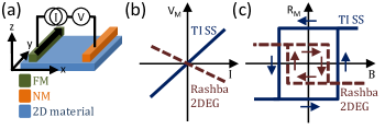
Figure 1: (a) Schematic of a spin injection/detection experiment on the Rashba 2DEG or the TI SS, the current is passed through FM - NM contacts and voltage between them is measured. The detected voltage is , where is the usual ohmic voltage drop and depends on the projection of the spin polarization onto the FM magnetization direction. (b) The variation of with injected current for FM magnetization along direction. The slope is negative for the Rashba 2DEG and positive for TI SS. (c) The step-like hysteresis of with magnetic field (B) sweep that tracks the magnetization of the FM contact. The hysteresis is different for the Rashba 2DEG and the TI SS.
The signature of spin-charge coupled dynamics manifest itself as a magnetoresistance effect in a spin injection/detection experiment shown schematically in Fig. 1(a). In the shown experimental setup, one FM and one NM electrodes are deposited on the surface of the material along the direction, and a spin polarized current is injected into the 2D material through the left FM electrode in the direction. The FM is magnetized along the direction, and the voltage drop is measured between the two electrodes as the FM magnetization direction is reversed. In this measurement geometry, there will be no variation of the charge and the spin density along the direction, i.e., parallel to the electrodes, so the voltage drop can be calculated by solving the coupled diffusion equations, Eq. 3 or Eq. 5, with the proper boundary conditions for the charge and the spin currents. From the conservation of electric charge, the current continuity equation can be written as , where is the particle current density ( times the charge current density, where is the electric charge) along the direction, which is given by . So, for an injected current , the boundary condition for the particle current density is , where is the width of the electrodes along the direction, and is the length between the two electrodes (assuming FM and NM electrodes are at and respectively). However, for the boundary condition of the component of the spin current density , only the contribution from the gradient of spin density should be considered, Burkov and Hawthorn (2010); Burkov, Núñez, and MacDonald (2004); Taguchi, Yokoyama, and Tanaka (2014). The FM injects a spin current density of to the left, where is the density of state spin polarization of the FM and is the -component of magnetization of the FM. The spin current extracted by the NM is zero for larger than the spin diffusion length, so we have and . In the static limit, the solution of the coupled diffusion equation with these boundary conditions will give the full electrochemical potential , from which the voltage drop can be calculated as , where is the density of states at the Fermi level.
The voltage drop between the two electrodes consists of two parts, , where the ohmic voltage drop is independent of the magnetization of the FM, and the magnetoresistive part depends on the FM magnetization direction. For Rashba 2DEG, is approximately given by:
(6)
where is the sheet resistance, is the 2D conductivity. For the SS of TI, is given by:
(7)
The voltage-current (V-I) characteristic is shown in Fig. 1(b) for FM magnetization along the direction (i.e. ) in case of both the Rashba 2DEG and the TI SSs. The voltage drop is linear with , and the slope which is the resistance is negative for a Rashba 2DEG and positive for SSs of a TI. The opposite sign of the slope for the two cases is related to the sign of the spin-charge coupling strength ; is negative for the Rashba 2DEG and positive for the TI SS. As, typically25 (25) is larger than , the slope is larger for TI SS than for Rashba 2DEG formed on the surface. The resistance between the FM and the NM electrodes will show a step-like hysteresis as the magnetic field direction is swept, as schematically shown in Fig. 1(b). For the Rashba 2DEG, a low resistance state will be observed for the ve magnetic field and a high resistance state will be observed for the ve magnetic field. However, for the TI SS, a higher resistance state will be detected for ve field and a lower resistance state will be detected for ve fields. The hysteresis of the resistance will follow the magnetization hysteresis of the FM electrodes (as ) with a coercive field value of the FM. The difference in the resistance is the measured spin signal in the experiment due to the current induced spin polarization of the TI SS.
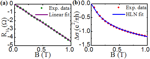
Figure 2: (a) Hall resistance with magnetic field perpendicular to the sample surface at K, solid line is the linear fit. (b) Change in conductivity with magnetic field perpendicular to the surface at K, solid line is the HLN fit.
In the experiment, we measure the spin signal for an MBE grown Bi2Te3 TI thin film of 4 nm thickness. The details of the growth and initial characterizations have been reportedRoy et al. (2013); Dey et al. (2014). The transport measurements are performed in a Physical Property Measurement System capable of cooling down to K with magnetic field up to T. The thin film is patterned in a Hall bar geometry with standard etching and lithography. The transverse Hall resistance and the longitudinal resistance are measured using Ti/Au contacts deposited on the patterned thin film. Figure 2(a) shows the Hall resistance of the thin film at K with magnetic field perpendicular to the sample surface. The Hall resistance is linear with a negative slope, indicating the carriers are electrons. The 2D carrier concentration obtained from the slope of the linear fit is cm-2. Such a high electron concentration indicates that both the surface and the bulk states are occupiedRoy et al. (2013); Dey et al. (2014, 2016). The conductivity obtained from the longitudinal resistance shows the signature of weak antilocalization (WAL). We plot in Fig. 2(b) the change in conductivity with magnetic field applied perpendicular to the surface at K. The sharp cusp near zero field is due to destruction of phase coherence of the electrons in an applied perpendicular field. The magnetoconductivity is explained with the Hikami-Larkin-Nagaoka (HLN) formulaHikami, Larkin, and Nagaoka (1980):
(8)
where is the phase coherence length, is the Planck’s constant and is a fitting parameter. From the HLN fitting shown in Fig. 2(b), we obtain nm and . Although, the value of implies that both the surface and the bulk states are coupled and behave like a single phase coherent channelRoy et al. (2013); Dey et al. (2014); it is possible that only the spin polarized surface state, and not the bulk states, contribute significantly to the spin signalLi, CH and van‘t Erve, OMJ and Robinson, JT and
Liu, Y and Li, L and Jonker, BT (2014); Dankert et al. (2015); Liu et al. (2015); Lee et al. (2015); Yang et al. (2016). In our thin film, the 3D electron concentration cm-3 is close to the saturated electron concentration cm-3 in Bi2Te3 that corresponds to the stabilized Fermi levelSuh et al. (2014). As the bulk Fermi level is very close to the Fermi level stabilized on the surface, the band-bending near the surface will be small causing negligible Rashba spin splitting of the quantum confined bulk states that will not contribute to the spin signal. It was shownYang et al. (2016) that, tuning Fermi level in the bulk gap will induce large band-bending near the surface that will cause large spin-splitting and give rise to opposite sign of the spin signal than that of TI SS.
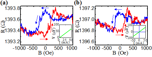
To detect the spin signal in our thin film, we have fabricated a measurement geometry, shown in Fig. 1(a), of dimensions m and m with Fe as the FM and Ti/Au as the NM contact. We evaporate a patterned MgO(1 nm)/Fe(20 nm) stack on the top surface of the Bi2Te3 thin film. The thin layer of MgO helps in resolving the issue of resistance mismatch between the metallic Fe and the TI thin film, as well as protects the SS of the TI from the ferromagnetic exchange interaction that can break the time reversal symmetry. The Fe contact is rectangular in shape with the easy axis lying in the -direction, and is capped with nm of Au. The magnetic field is applied parallel to the surface along the length of the Fe bar (along the easy axis), perpendicular to the direction of the current as shown in Fig. 1(a). Two terminal V-I measurements are recorded at each applied magnetic field as we sweep the field. The resistance at each magnetic field is obtained from the linear V-I characteristic, two of such data are shown in the insets of Fig. 3(a) and 3(b). Two sets of measurements are performed at K to obtain the resistance at different magnetic fields, one with the applied current ramped from zero to a positive value, and another with the current ramped from negative to a positive value.
Figure 3: Magnetic field () dependence of resistance between a FM and a NM contact deposited on the surface of the Bi2Te3 thin film, R obtained from characteristic at each field (one such measurement at zero field is shown in the inset of each figure) for current values of (a) A to A, (b) A to A. The resistance shows hysteresis that mimics that of magnetization of the FM contact.
Figure 3(a) shows the resistance with the magnetic field sweep from a positive field of Oe to a negative field of Oe and back to a positive field of Oe. In the first set of measurements shown in Fig. 3(a), the resistance is obtained from the V-I characteristic with current values of A to A. The inset of Fig. 3(a) shows one such V-I plot at zero field. From the hysteresis of resistance with applied field shown in Fig. 3(a), it is seen that a high resistive state is obtained at positive magnetic field, while a low resistive state is obtained at negative field. This is consistent with the theory which predicts the same resistive state for the TI SSs, but a different resistive state for the Rashba 2DEG, as shown in Fig. 1(c). Similar hysteresis is observed in the second set of measurements as shown in Fig. 3(b), where we have obtained the resistance from V-I characteristic with current values of A to A. The inset of Fig. 3(b) shows one such V-I plot at zero magnetic field. As seen in Fig. 3(b), the resistance is higher for positive magnetic fields and lower for negative fields, consistent with that of Fig. 3(a). The hysteresis resembles the one in Fig. 3(a) showing a similar coercive field value. The hysteresis loop observed in the resistance versus applied magnetic field is almost square shape with a coercive field value of about Oe. The hysteresis loop is shifted towards a negative field value, which can be due to the exchange bias between ferromagnetic Fe and the anti-ferromagnetic oxide of Fe. Also, the local peaks seen in the resistance near the coercive field values can be attributed to the magnetic domain reversal in the multi-domain Fe contactLi, CH and van‘t Erve, OMJ and Robinson, JT and
Liu, Y and Li, L and Jonker, BT (2014). However, the hysteresis overall shows a single step-like behavior when the FM magnetization direction changes from to and vice-versa. The observed hysteresis in the resistance measured both for positive and negative currents show that the magnetoresistive voltage drop is directly proportional to the magnitude and the sign of the applied current giving a linear V-I characteristics. This consideration rules out the possibility that the observed hysteresis is due to the anisotropic magnetoresistance or the anisotropic tunnel magnetoresistance of the Fe contacts, as the voltage drop due to these effects are only proportional to the magnitude of current and not the directionLi, CH and van‘t Erve, OMJ and Robinson, JT and
Liu, Y and Li, L and Jonker, BT (2014); Tang et al. (2014); Dankert et al. (2015). Also, the Hall effect from the film due to the perpendicular component of fringe fields of the Fe, or the spin Hall effect of the bulk can be excluded as these effects will give rise to a signal much smaller than that we have observedLi, CH and van‘t Erve, OMJ and Robinson, JT and
Liu, Y and Li, L and Jonker, BT (2014); Tang et al. (2014); Dankert et al. (2015). Further, the anomalous Hall effect or the anomalous Nernst effect of the Fe contact is excluded by doing a controlled experiment. The hysteresis of resistance with magnetic field matches with magnitude (that we show next) and the sign of that for the TI SS while being opposite in sign and higher in magnitude than that of Rashba 2DEG. So, we exclude the possibility that the spin signal is due to a Rashba 2DEG formed at the surface or the interface. Hence, both sets of measurement, shown in Fig. 3, indicate that the observed spin signal is indeed of the nature predicted in theory due to the SS of the Bi2Te3 thin film.
We obtain the value of from the experiment. The theoretical value of for TI SSs can be calculated from Eq. 7, using for the TI SSs:
(9)
From the carrier concentration*[Assumingtwo2Dsurfacestatesandatleasttwodegeneratequasi-2D(becauseofourthinfilm)bulkstatesbeingpopulated; i.e.atleast4statesbeingfilled; anupperlimitof$k_F$isestimatedfromthecarrierconcentration$n_c$using$k_F=\sqrt{\pin_c}$][]26, the estimated nm-1. Using the values m and for FeLi, CH and van‘t Erve, OMJ and Robinson, JT and
Liu, Y and Li, L and Jonker, BT (2014); Li et al. (2016a), we obtain . The theoretical estimate agrees well with the experimental value, indicating that SS in the thin film mainly contribute to the spin signal.
In conclusion, we derived the coupled spin-charge transport equations from quantum kinetic theory for both the Rashba 2DEG and the TI SS. Solving the differential equations with proper boundary conditions, the behavior of the resistance between a FM and a NM contact is obtained as a function of the magnetization of the FM. We experimentally measured the resistance between a FM and a NM contact on the surface of a MBE grown Bi2Te3 thin film, which shows hysteresis with the applied field tracking that of the magnetization of the FM contact. The experimental value of the difference in resistance on reversing the FM magnetization direction agrees well in magnitude and sign with that of a TI SS, providing evidence of spin polarized SS in the thin film.
This work is supported by the NRI SWAN and the NSF NNCI program.
Supplementary Material
S1: Theoretical model
Here, we are going to derive the coupled spin and charge transport equations for the Rashba two-dimensional electron gas (2DEG) as well as the surface state (SS) of a topological insulator (TI) from quantum kinetic equation under the diffusive approximation. We consider a general Hamiltonian for 2DEG with Rashba spin splitting ()Liu and Sinova (2012); Burkov, Núñez, and MacDonald (2004):
(S1)
where is the effective mass, is the in-plane momentum (), is the identity matrix, with ’s being the Pauli matrices (bold letter indicating a matrix in spin space) and is the strength of the SOC. The Hamiltonian for the SS of a TI readsBurkov and Hawthorn (2010); Liu and Sinova (2013):
(S2)
with being the Fermi velocity of the SS. As can be obtained from by taking and , we will write down the kinetic equations for the more general Hamiltonian first and then obtain the one for afterwards by the appropriate substitution.
The quantum kinetic equation can be written in terms of angular distribution function (where , is the in-plane position and is the time) and density matrix asLiu and Sinova (2012, 2013):
(S3)
Here, is any Hamiltonian, is the velocity operator, and is the momentum scattering time assuming random spin-independent delta-correlated impurity potential. The quantities and are averages over the energy and are functions of , where the average of any function is with being the Fermi-Dirac distribution and being the energy dispersion of the Hamiltonian . At zero temperature, peaks the value at the constant energy Fermi surface, so becomes only function of and the Fermi momentum (as , the Fermi wave vector, at zero temperature). By writing (where ) and (where ), and taking trace of Equation (S3) after multiplying by , where , and using the fact that , we will get:
(S4)
Equation (S4) can be written in a matrix form in the Fourier space of (Fourier transformed and ) as () with the matrix given by:
(S5)
Here, , and . There were typos in previous reportsLiu and Sinova (2012, 2013) in the literature that we have corrected here in Equation (S4), (S5), and (S6) (Equation (2) in the main article). Now, we consider uniform charge and spin density along the direction, i.e. , so becomes:
(S6)
Using the fact that and , the spin-charge dynamic equation can be written as , where . It was shown thatLiu and Sinova (2012, 2013), in case of , the diffusion of the - and -components of spin are decoupled from the charge and -component of spin transport. So, we are interested in the components of the diffusion matrix that will give rise to spin-charge coupled diffusion equations.
.1 Rashba 2DEG
Assuming , we obtain , and , where, is the Fermi velocity. The terms are all zero in the diffusive limit, i.e., under the conditions , , ( is the mean free path for the Rashba 2DEG), and with the assumption that the spin splitting is smaller than the Fermi energy, i.e., . These conditions also implies and (as since , ). With these assumptions, we show that:
(S7)
Similarly, are all zero in the diffusive approximation. So we have obtained that the - and -components of spins are decoupled from charge and -component of spin. Now, to get the spin-charge coupled transport, we evaluate the other terms:
(S8)
Similarly, and .
From (), the spin-charge coupled diffusion equation can be written as , where is a 22 identity matrix, is a 22 diffusion matrix for charge and spin. The charge density and spin density , so . The coupled diffusion equation in Fourier space becomes:
(S9)
Now, inverse Fourier transforming back to time and real-space variation (i.e. and ), we get:
(S10)
whcih matches with the one derived from Kubo formalismBurkov, Núñez, and MacDonald (2004). Here, charge diffusion coefficient , spin diffusion coefficient , spin relaxation time and spin-charge coupling strength .
.2 Surface state of a TI
The Hamiltonian of the SS of a TI, given by Equation (S2), can be obtained from Equation (S1) by the substitution and , so the corresponding matrix will be given by Equation (S6) with , (as at 2 K) and . As the denominator of is a function of , by the symmetry of the trigonometric function in the four quadrants (, the terms are all zero after angular integration. So, the spin dynamics in the directions are decoupled from charge transport, while the charge and -component of spin are coupled. To get the spin-charge coupled dynamics, we evaluate the terms under diffusive approximation, i.e. and ( is the mean free path for the SS, in this case), and i.e. (). Under these conditions, we obtain:
(S11)
Similarly,
(S12)
and
(S13)
So, the matrix diffusion equation in Fourier space reads:
(S14)
Now, using the value of , and inverse Fourier transforming back to time and real-space variation (i.e. and ), we get the coupled diffusion equation:
(S15)
where, , , and . These coupled equations are same as obtained previouslyBurkov and Hawthorn (2010).
.3 Solution of diffusion equations
In the static limit, we write the coupled spin-charge diffusion equation for both the Rashba 2DEG and the TI SS in the following general form:
(S16)
with and () replaced by appropriate values for Rashba 2DEG or TI SS in specific cases.
Now, we solve the equation for a charge current injected along the -direction with a finite width of the injecter contacts. As, the particle current density along the direction is given by , and the injected particle current density is (), we get from the first of the Equation (S16):
(S17)
Inserting Equation (S17) into the second of Equation S(16), we get:
(S18)
where we have introduced . Now, we follow the derivation on Ref.Taguchi, Yokoyama, and Tanaka (2014) [5], and make the substitution , to get the new differential equation , or . Using Equation (S17), we calculate the voltage drop between the two contacts situated at a distance as:
(S19)
The first term gives the ohmic voltage drop and the second term is due to the spin current injection. In the boundary condition of the component of the spin current density , only the contribution from the gradient of spin density should be considered, Burkov and Hawthorn (2010); Burkov, Núñez, and MacDonald (2004); Taguchi, Yokoyama, and Tanaka (2014). The FM injects a spin current density of at and no spin current is injected or extracted by the NM at assuming (order of m) is much larger than spin diffusion length (order of nm). So, using and in Equation (S19), we get:
(S20)
where is the sheet resistance, is the 2D conductivity.
For, Rashba 2DEG, using and (where )and , we get implying (as ). Now using the value of and , we obtain:
(S21)
For the TI SS, using , (where ), and , we get and
(S22)
S2: Controlled experiments
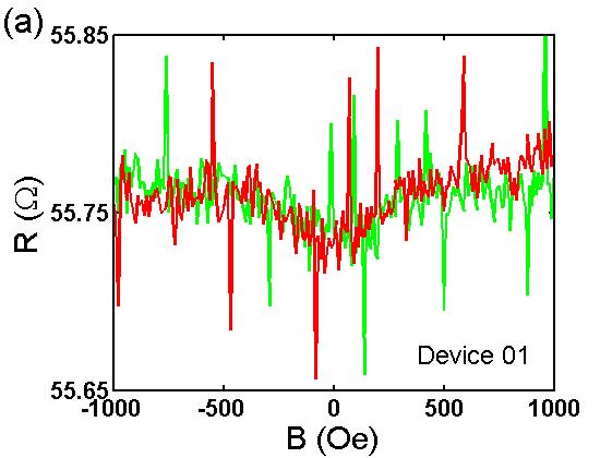
Figure S1: Two-point magnetoresistance between a ferromagnetic MgO/Fe and a nonmagnetic Ti/Au contact deposited on the surface of a 10 nm thick Au film shows no hysteresis. Data for two separate devices are given in (a) and (b).
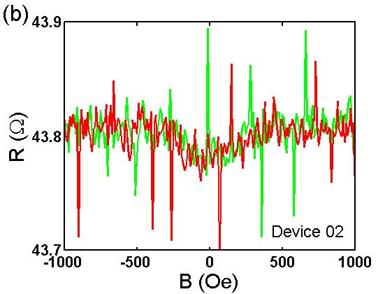
As a supporting evidence to show that the observed spin signal is indeed arising from the Bi2Te3 thin film, and not due to other spurious effects such as anisotropic magnetoresistance or anisotropic tunnel magnetoresistance or the anomalous Hall effect or the anomalous Nernst effect in the ferromagnetic Fe contact, we repeat the experiments on Au film of 10 nm thickness. We fabricated identical two probe device with ferromagnetic MgO/Fe and nonmagnetic Ti/Au contacts of the same dimensions and thicknesses of the ones we used for measurement on Bi2Te3. As shown in Figure S1, the measured resistance in an applied magnetic field is parabolic, which is a characteristic of the Au film, and no hysteresis with field sweep is observed. This results confirms none of the spurious effects in Fe is responsible for the observed hysteresis in the resistance with magnetic field sweep in our Bi2Te3 sample. So, we conclude that the hysteresis observed in the measurement on the TI thin film is due to the spin polarized surface state of Bi2Te3.
References
Zhang et al. (2009)H. Zhang, C.-X. Liu,
X.-L. Qi, X. Dai, Z. Fang, and S.-C. Zhang, Nature
Physics 5, 438 (2009).
Xia et al. (2009)Y. Xia, D. Qian, D. Hsieh, L. Wray, A. Pal, H. Lin, A. Bansil,
D. Grauer, Y. S. Hor, R. J. Cava, and M. Z. Hasan, Nature
Physics 5, 398 (2009).
Chen et al. (2009)Y.-L. Chen, J.-G. Analytis,
J.-H. Chu, Z.-K. Liu, S.-K. Mo, X.-L. Qi, H.-J. Zhang, D.-H. Lu, X. Dai, Z. Fang, S.-C. Zhang, I.-R. Fisher, Z. Hussain, and Z.-X. Shen, Science 325, 178
(2009).
Mellnik et al. (2014)A. Mellnik, J. Lee,
A. Richardella, J. Grab, P. Mintun, M. Fischer, A. Vaezi, A. Manchon, E.-A. Kim, N. Samarth, et al., Nature 511, 449 (2014).
Li, CH and van‘t Erve, OMJ and Robinson, JT and
Liu, Y and Li, L and Jonker, BT (2014)Li, CH and van‘t
Erve, OMJ and Robinson, JT and Liu, Y and Li, L and Jonker, BT, Nature
nanotechnology 9, 218
(2014).
Tang et al. (2014)J. Tang, L.-T. Chang,
X. Kou, K. Murata, E. S. Choi, M. Lang, Y. Fan, Y. Jiang, M. Montazeri, W. Jiang, Y. Wang, L. He, and K. L. Wang, Nano Letters 14, 5423 (2014).
Ando et al. (2014)Y. Ando, T. Hamasaki,
T. Kurokawa, K. Ichiba, F. Yang, M. Novak, S. Sasaki, K. Segawa, Y. Ando, and M. Shiraishi, Nano Letters 14, 6226 (2014).
Dankert et al. (2015)A. Dankert, J. Geurs,
M. V. Kamalakar, S. Charpentier, and S. P. Dash, Nano Letters 15, 7976
(2015).
Lee et al. (2015)J. S. Lee, A. Richardella,
D. R. Hickey, K. A. Mkhoyan, and N. Samarth, Phys.
Rev. B 92, 155312
(2015).
de Vries et al. (2015)E. K. de Vries, A. M. Kamerbeek, N. Koirala,
M. Brahlek, M. Salehi, S. Oh, B. J. van Wees, and T. Banerjee, Phys. Rev. B 92, 201102 (2015).
Yang et al. (2016)F. Yang, S. Ghatak,
A. A. Taskin, K. Segawa, Y. Ando, M. Shiraishi, Y. Kanai, K. Matsumoto, A. Rosch, and Y. Ando, Phys. Rev. B 94, 075304 (2016).
Roy et al. (2013)A. Roy, S. Guchhait,
S. Sonde, R. Dey, T. Pramanik, A. Rai, H. C. P. Movva, L. Colombo, and S. K. Banerjee, Applied Physics Letters 102, 163118 (2013).
Dey et al. (2014)R. Dey, T. Pramanik,
A. Roy, A. Rai, S. Guchhait, S. Sonde, H. C. P. Movva, L. Colombo, L. F. Register, and S. K. Banerjee, Applied Physics Letters 104, 223111 (2014).