Graphene Phase Modulator
Abstract
We demonstrate a 10Gb/s Graphene Phase Modulator (GPM) integrated in a Mach-Zehnder interferometer configuration. This is a compact device, with a phase-shifter length of only 300m, and 35dB extinction ratio. The GPM has modulation efficiency of 0.28Vcm, one order of magnitude higher compared to state-of-the-art depletion p-n junction Si phase modulators. Our GPM operates with 2V peak-to-peak driving voltage in a push-pull configuration, and it has been tested in a binary transmission of a non-return-to-zero data stream over 50km single mode fibre. This device is the key building block for graphene-based integrated photonics, enabling compact and energy efficient hybrid Si-graphene modulators for telecom, datacom and other applications.
Optical communication systems for telecom and datacom implement high-order digital modulation schemes, such as amplitude or phase-shift keying, in order to enhance spectral efficiency and increase the data transmission capacity of telecommunication networksSeimetz2009 . This is possible by encoding several bits of information in fewer symbols, leading to the same amount of data, but transmitted at lower speed, resulting in reduced spectral bandwidth. Spectral narrowing is a key technique for optimizing data capacity in modern wavelength-division multiplexing (WDM)Nakazawa2010 allowing higher data rates, improved spectral efficiency and robust tolerances to transmission impairments, such as chromatic dispersionSeimetz2009 .
The modulator is a key component in optical communicationsAgrawal2010 . To encode the information in complex modulation formats, phase modulation (PM) is neededSeimetz2009 . In integrated Si photonics, this is achieved by exploiting the free-carriers plasma dispersion effectSoref1987 , whereby changes in electron and hole densities result in changes in the Si refractive index and absorption. In state-of-the-art Si modulatorsXiao2013 ; Streshinsky2013 ; Denoyer2015 ; Reed2013 ; Dong2012 ; Fresi2016 ; Milivojevic2013 the complex index change can be driven by p-n junctionsXiao2013 ; Streshinsky2013 ; Denoyer2015 ; Reed2013 ; Dong2012 ; Fresi2016 or capacitorsMilivojevic2013 built in Si waveguides, and applying a voltage to deplete or accumulate free-carriers interacting with the propagating light. High-speed for simple and complex modulation formats has been demonstratedXiao2013 ; Streshinsky2013 ; Denoyer2015 ; Reed2013 ; Dong2012 ; Fresi2016 ; Milivojevic2013 either with a depleted p-n junction under reverse biasXiao2013 ; Streshinsky2013 ; Denoyer2015 ; Reed2013 ; Dong2012 ; Fresi2016 , or with a Si-insulator-Si (SIS) capacitorMilivojevic2013 operating in the accumulation regime. However, the Si free-carrier effect in the depleted p-n junctionSoref1987 typically requires mm-size devices for accumulating a -phase shiftReed2013 with a 1-3V driving voltage. This limits the modulation efficiency, defined as the product of the -phase-shift voltage and length (VπL)Reed2008 , and increase energy consumption (energy per bit)Miller2012 . Another challenge is that plasma dispersion is always accompanied by absorptionSoref1987 . As a result, there is a tradeoff between optical loss, VπL and footprint, since higher free carriers densities with stronger plasma dispersion come at the expense of increased optical absorptionReed2008 or limited dynamic range, i.e. the maximum intensity or phase change for a given driving voltageReed2008 . Therefore, novel solutions with increased VπL, reduced optical loss, and miniaturized footprints are needed.
Graphene is appealing for photonics and optoelectronics because it offers a wide range of advantages compared to other materials, such as Si and other semiconductorsBonaccorso2010 ; Kim2011 ; Ferrari2015 ; CastroNeto . In particular, it is ideally suited for integration into Si photonicsBonaccorso2010 ; Hanson2008 ; Mak2008 due to its large optical modulationLiu2011 ; Liu2012 ; Hu2016 ; Phare2015 ; Sorianello2015 , broadband photodetectionKoppens2014 ; Goykhman2016 , high-speed operationPhare2015 ; Koppens2014 , and CMOS (complementary metal oxide semiconductor) compatibilityLiu2011 ; Liu2012 ; Hu2016 ; Phare2015 ; Sorianello2015 ; Koppens2014 ; Goykhman2016 . To date, several graphene based amplitude modulators have been reported based on electro-absorptionLiu2011 ; Liu2012 ; Hu2016 ; Phare2015 . However, graphene phase modulators (GPMs) are necessary for all functionalities requiring phase change, such as binary and complex modulation formats, switching, phased arrays, etc. GPMs are also expected to have an improved efficiency-loss figure of merit compared to Si based modulatorsSorianello2015 . Graphene integration with Si photonics opens a new paradigm for developing compact, efficient and low-loss integrated PMs outperforming state-of-the-art Si devicesXiao2013 ; Streshinsky2013 ; Denoyer2015 ; Reed2013 ; Dong2012 ; Fresi2016 ; Milivojevic2013 . Due to its unique opto-electronic properties, optical losses in single layer graphene (SLG) can be electrically suppressed due to Pauli blockingWang2008 ; Falkovski2008 ; Stauber2008 . This modulates the absorption, with a refractive index change much larger than that the free carriers effect in SiSorianello2015 . SLG on Si waveguides with effective refractive index (i.e. the ratio between the light phase velocity in the waveguide and in vacuum) changes larger than 10-3 have been demonstratedSorianello2016 , about ten-times larger than state-of-the-art Si p-n junction waveguides in depletion modeReed2008 . Consequently, SLG can provide a unique combination of strong electro-refractive effect and optical transparency when operated in the Pauli blocking regime.
Here we demonstrate a GPM included in a Mach-Zehnder interferometer (MZI),Fig.1a, in which PM is realized in the form of a Si-insulator-SLG (SISLG) capacitor and the Si waveguide is used as a gating electrode to the SLG, Fig.1b). By applying a bias to the capacitor, charge is accumulated on the SLG electrode, shifting its Fermi level, EF, and modifying its complex conductivityWang2008 ; Falkovski2008 ; Stauber2008 ; Sorianello2016 . In this way, both the effective index and the optical loss of a SLG-functionalized Si waveguide can be tunedSorianello2016 . If the SLG is doped beyond the Pauli blocking condition (E0.4eV at 1.55m), the device operates in the low-loss ”transparency” region, where the only loss contribution is given by the Si waveguide propagation loss without SLG. In this regime, PM is dominant with respect to amplitude changesSorianello2015 , with an enhanced modulation efficiency (VπL0.26Vcm)Sorianello2015 compared to typical Si photonics modulators operating in depletion mode (VπL2Vcm)Reed2008 .
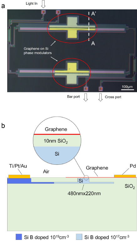
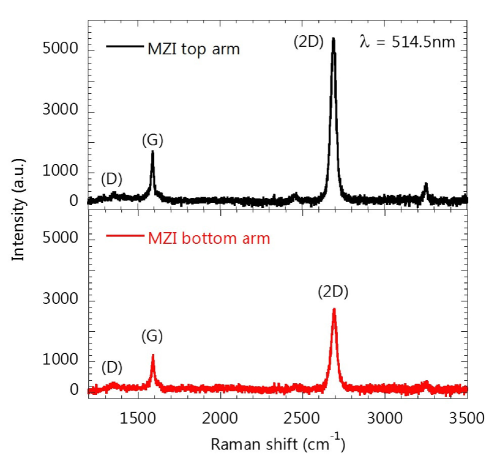
Our device is fabricated in a standard Si photonics platform using a Si-on-insulator (SOI) substrate (see Methods). The photonic structure consists of a balanced MZI with 3dB multimode interference (MMI) couplersSoldano1995 to split and combine the optical beam, and grating couplersRoelkens2006 to couple light in and out of the device, Fig.1a). The Si waveguide is designed to support a single transverse electric (TE) in-plane polarized optical mode. The waveguide is B doped to reduce the Si resistance and achieve high-speed operationReed2008 . SLG is grown by chemical vapor deposition (CVD) and then wet transferred (see Methods) onto 10nm planarized Si dioxide (SiO2) top cladding, Fig.1b). We use different SLG lengths onto the two MZI arms (300 and 400m) to intentionally introduce a bias phase difference in the balanced interferometer structure for characterization purposes. The quality and uniformity of SLG after device fabrication are characterized by Raman spectroscopy (see Methods). The spectra show negligible D to G intensity ratio (Fig.2), indicating that no significant degradation and/or defects are introduced during the fabrication processCancado2011 ; Bruna2014 . From the Raman G peak position, Pos(G), full width at half maximum, FWHM(G), and intensity and area ratios of D and G peaks we estimateBasko2009 ; Das2008 E100meV (200meV) at the longer top (shorter bottom) arms of the MZI.
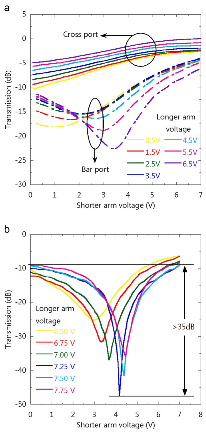
To test the electro-refractive effect, we first perform static characterizations by measuring the MZI output power as a function of bias applied to the GPMs on both MZI arms, Fig.3. A 1550nm laser source is coupled to the MZI input using a SMF, while the optical power at the MZI outputs, i.e the bar and cross ports, is collected with a similar fibre and monitored by a power meter (see Methods). In our balanced MZI the cross port is expected to be at maximum when the phase difference between the two arms is zero, while the bar port tends to be at zero powerBorn1970 . We measure an output power difference5dB between the two ports when no voltage is applied. We assign this imbalance to the difference in absorption and phase accumulation between the two MZI arms caused by the different SLG lengths, doping and defects, Fig.2. By applying a bias to the SISLG capacitors, we decrease the bar port power to zero, with an extinction ratio (ER, ratio between maximum and minimum of the transmission)35dB, Fig.3b). This is due to the phase change introduced in the two arms by electrical gating the SLGs. The 35dB ER is due to a phase difference between the two arms approaching , and this is evidence of interferometric behaviorBorn1970 , with a considerable electro-refractive effect. In particular, we measure V7.25V on the 400m SISLG capacitor, corresponding to VπL0.28, very close to the theoretical predictionSorianello2015 . This is at least a 8-fold improvement compared to state-of-the-art p-n junction based Si MZI modulatorsDenoyer2015 . The VπL efficiency can be doubled by using a SLG-insulator-SLG phase modulator taking advantage of the effect of two SLGs on the effective index of the waveguideSorianello2015 .
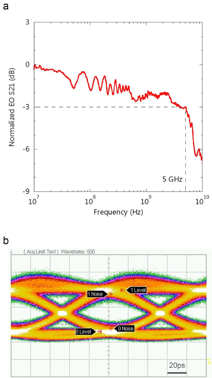
To test the modulator electro-optical (EO) bandwidth and operation speed, we first characterize the frequency response by using an electrical vector network analyzer (VNA) (see Methods). We measure a 3dB roll-off frequency of 5GHz at 4V, Fig.4a). The bandwidth is limited by the RC time constant primarily due to the SISLG capacitor and the series resistances. The overall capacitance C is the sum the capacitor on top of the waveguide core (CfF/m, where is the vacuum dielectric constant, is the SiO2 dielectric constant, wwg is the waveguide core width and tox the oxide thickness) and the parasitic capacitor Cp due to the SLG overlap on the Si slab (CfFm, where wm is the overlap and tp the oxide thickness between SLG and Si slab). Cp depends on the alignment between transferred SLG and waveguide core, and it can contribute up to 20% of the overall C. The series resistance, R, stems from different contributions: the Si resistance (Rsi, estimated5km, see Methods), the SLG lead from the waveguide core to the metal contact, Rg (estimated1km, see Methods), the metal to SLG contact resistance, Rc. The latter is estimated as10km by using a transfer length measurement (TLM) on test samples (see Methods). In our device, the metal/SLG contact resistance is the main factor limiting the radio-frequency (RF) bandwidth. This can be improved by reducing Cp and Rc. Contact resistances down to 100m have been reportedLeong2014 , such values would increase the RF bandwidth up to 30GHz and beyond, leading to high frequency operations comparable with state-of-the-art modulatorsXiao2013 ; Streshinsky2013 ; Denoyer2015 ; Reed2013 ; Dong2012 ; Fresi2016 ; Milivojevic2013 .
We now discuss the optical response when the MZI modulator is driven by a non-return-to-zero (NRZ) signalSeimetz2009 . We measure the MZI NRZ eye diagram with the two GPMs biased at 3.5V and operating in push-pull configuration, with 2V peak-to-peak and 231-1 pseudorandom binary sequence (PRBS)Agrawal2010 signals. Fig.3b plots an open eye diagram at 10Gb/s with4dB ER and6dB signal-to-noise ratio (SNR). With a random bit stream, the individual GPM average energy consumption is given byMiller2012 C(V)2/4, where V is the voltage variation driven to the contacts in order to charge/discharge the GPM capacitance. In our device, we get1pJ/bit. The energy consumption could be reduced with the SLG-insulator-SLG configuration, potentially allowing us to halve the driving voltageSorianello2015 .
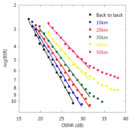
We then carry out bit error rate (BER) measurements when the NRZ signal is transmitted in a standard single mode fiber (SMF) over different distances, Fig.5. We measure the BER as a function of optical signal-to-noise ratio (OSNR) in back-to-back configuration, and after propagation in SMF spools of different lengths from 10 to 50km. We have error free operation (BER10-10) up to 30km, while at longer propagation distances a BER floor appears. However, considering the state-of-the-art systems currently employing a soft-decision forward error correction (SD-FEC)Infinera2015 , with overhead in the 7-25% range, and enabling a pre-FEC BER threshold up to 3.4x10⁻² or even higherRahman2015 , our modulator exhibits error free operation up to 50km.
In summary, we demonstrated a graphene-silicon phase modulator operating in the GHz regime. We included the GPM in a MZI device demonstrating a static modulation depth of 35dB and modulation efficiency of 0.28Vcm, outperforming state-of-the-art Si-based p-n junctions and comparable to the SIS-capacitor based Si modulators. The modulator operates at 10Gbit/s, showing an open eye diagram and error free transmission over 50km single mode fibre. These results pave the way to the realization of graphene modulators for a wide range of telecom applications where the phase modulation is crucial.
We acknowledge funding from the Graphene Flagship Project ID: 696656, ERC Grant Hetero2D and EPSRC Grants EP/ 509 K01711X/1, EP/K017144/1, EP/N010345/1, EP/M507799/ 5101 and EP/L016087/1. We acknowledge Graphenea for the provision of CVD samples.
I Methods
The Si photonic device is prepared on the IMEC iSiPP25G Si on insulator (SOI) platformAbsyl2015 . The MZI interferometer is based on Si ridge waveguides with 60nm slab and a core cross-section 480nm220nm. SLG is placed on the Si waveguide separated by a 10nm spacer of high quality thermal SiO2. Graphene is grown by CVD on Cu foils, as described in Ref.Li2009 , and then transferred onto our Si samples following the procedure described in Ref.Zurutuza2015 . Graphene patterning is done by using a bilayer stack of PMMA/IX845, while etching is done using conventional O2-plasmas. The metal contacts on SLG and Si are processed separately in two consecutive steps. SLG is contacted with a single 50nm thick Palladium (Pd) layer, while the metal contact on Si consists of a Titanium (Ti)/Platinum (Pt)/Gold (Au) stack with thickness 20nm/20nm/30nm deposited on the Si surface after HF cleaning to remove the native SiO2. Contact resistance and mobility are evaluated on different samples with equivalent processing. Typically values of 10km are extracted at the charge neutrality point using the TLM methodPolitou2016 ; Politou2017 , with mobility1500cm2V-1s-1.
After device fabrication, the quality and uniformity of SLG at both arms of the MZI is monitored by Raman spectroscopy using a Horiba LabRam Evolution Raman spectrometer with 514.5nm laser and optical power below 0.1mW. The Raman spectra from the top and bottom arms (GPMs) of the MZI are normalized to the Si Raman peak at 521cm-1. The 2D peak is a single sharp Lorentzian with full width at half maximum FWHM(2D)36cm-1 (39cm-1) at the top (bottom) arm of the MZI, a signature of SLGFerrari2013 . The spectra show negligible I(D)/I(G)0.12 (0.16), indicating that no significant degradation and/or defects are introduced during the fabrication processCancado2011 . We estimate a defects density2.31010cm-2 and6.51010cm-2 at top and bottom GPMs respectivelyCancado2011 ; Bruna2014 . Pos(G) is1592 cm-1 (1593cm-1), with FWHM(G)17cm-1 (19cm-1). The 2D peak position, Pos(2D) is2691cm-1 (2693cm-1), while the 2D to G peak intensity and area ratios I(2D)/I(G) and A(2D)/A(G), are3.7 (2.6) and 8.2 (5.3), indicating a p-doping100meV (200meV)Basko2009 ; Das2008 at the top (bottom) arm of the MZI. These correspond to carriers concentrations11012cm-2 (2.3 cm-2)Das2008 .
Rsi is evaluated by numerical electrical simulations of the GPMs cross section with a commercial-grade device simulator that self-consistently solves the Poisson and drift-diffusion equationslumerical . We use Si doping and resistivity as obtained from the IMEC iSiPP25G technologyAbsyl2015 . For SLG, we estimate a sheet resistance 400 when the SLG is gated beyond the Pauli blocking condition (E0.4eV). For E0.4eV the carrier concentration exceeds 1.31013cm-2 (, where ns is the carrier concentration, the bar Planck constant and vF is the Fermi velocityWang2008 ), the mobility degradation from the ungated value is negligibleHirai2014 . As the SLG lead from the waveguide core to the metal contact is 2.5m, Rg can be estimated400m=1km.
The input/output optical coupling is obtained through cut single mode fibres with cleaved output surfaces. The input fibre is connected to the laser source with a fibre polarization controller to maximize the input coupled light. We use a tunable external cavity laser fixed at 1550nm. The output fibre is connected to a high sensitivity power meter to measure the static characteristics in Fig.3. Two ground signal (GS) high frequency probes apply DC and RF signals to the two MZI GPMs. For small-signal RF bandwidth measurements we use an electrical VNA. Its output is connected through a 50 matched high frequency cable to the GS probe contacting the GPM. We use a bias-tee to combine RF power and DC bias. We set a DC bias of 4V and an RF power of -17dBm. The light at the output of the MZI is modulated by the RF signal from the VNA and collected by a low noise, high frequency photodetector connected to the VNA input. The signals for the eye diagram and BER measurements are generated by a pattern generator (PG) and collected with a digital sampling oscilloscope (eye diagram) and a BER tester. The PG provides the 231-1 pseudorandom binary sequence (PRBS) at 10Gb/s. The signal and inverted signal are sent to the two GPMs through the RF cable and bias-tee. We use the optical input of the oscilloscope to collect the light out of the MZI GPM and visualize the eye diagram of Fig.4b. For BER evaluation, we used a high frequency photo-receiver collecting the light at the output of the modulator and connected to the BER tester electrical input.
References
- (1) Seimetz, M. High-Order Modulation for Optical Fiber Transmission (Springer, 2009).
- (2) Nakazawa, M., Kikuchi, K., and Miyazaki, T. High spectral density optical communication technologies (Springer, 2010).
- (3) Agrawal, G. P. Fiber-Optic Communication Systems, (Wiley, 2010).
- (4) Soref, R. & Bennet, B. Electro-optical effects in Silicon. IEEE J. Quantum Electron. 23, 123 (1987).
- (5) Xiao, X. et al. High-speed, low-loss Silicon Mach-Zehnder modulators with doping optimization. Opt. Express 21, 4116 (2013).
- (6) Streshinsky, M. et al. Low power 50 Gb/s Silicon traveling wave Mach-Zehnder modulator near 1300 nm. Opt. Express 21, 30350 (2013).
- (7) Denoyer, G. et al. Hybrid Silicon Photonic Circuits and Transceiver for 50 Gb/s NRZ Transmission Over Single-Mode Fiber. IEEE J. Lightwave Techn. 33, 15 (2015).
- (8) Reed, G. T. et al. Recent breakthroughs in carrier depletion based silicon optical modulators. Nanophotonics 3, 229 (2013).
- (9) Dong, P. et al. 50-Gb/s silicon quadrature phase-shift keying modulator. Opt. Express 19, 21181 (2012).
- (10) Fresi, F. et al. Reconfigurable Silicon Photonics Integrated 16-QAM Modulator Driven by Binary Electronics. IEEE J. Sel. T. Quant. 22, 1 (2016).
- (11) Milivojevic, B. et al. 112Gb/s DP-QPSK transmission over 2427km SSMF using small size silicon photonics IQ modulator and low power CMOS driver. Optical Fiber Communication Conference/National Fiber Optic Engineers Conference 2013, OSA Technical Digest (online), paper OTh1D.1 (2013).
- (12) Reed, G. T. Silicon photonics; the state of the art. (Wiley, 2008).
- (13) Miller, D. A. B. Energy consumption in optical modulators for interconnects, Opt. Express 20, A293 (2012).
- (14) Bonaccorso, F., Sun, Z., Hasan, T., and Ferrari, A. C. Graphene photonics and optoelectronics. Nature Photon. 4, 611 (2010).
- (15) Kim, K. et al., A role for Graphene in Silicon-based semiconductor devices. Nature 479, 338 (2011).
- (16) Ferrari, A. C et. al., Science and technology roadmap for graphene, related two-dimensional crystals, and hybrid systems. Nanoscale 7, 4598 (2015).
- (17) Castro Neto, A. H., Guinea, F., Peres, N. M. R., Novoselov, K. S., and Geim, A. K. The electronic properties of graphene. Rev. Mod. Phys. 81, 109 (2009).
- (18) Hanson, G. W. Dyadic Green’s function and guided surface waves for a surface conductivity model of Graphene. J. Appl. Phys. 103, 064302 (2008).
- (19) Mak, K. F. et al. Measurement of the optical conductivity of graphene. Phys. Rev. Lett. 101, 196405 (2008).
- (20) Liu, M. et al. A graphene-based broadband optical modulator. Nature 474, 64 (2011).
- (21) Liu, M. et al. Double-layer graphene optical modulator. Nano Lett. 12, 1482 (2012).
- (22) Hu, Y. et al. Broadband 10 Gb/s operation of graphene electro-absorption modulator on silicon. Laser & Photonics Reviews 10, 307 (2016).
- (23) Phare, C. T. et al. Graphene electro-optic modulator with 30 GHz bandwidth. Nature Photon. 9, 511 (2015).
- (24) Sorianello, V. et al. Design optimization of single and double layer Graphene phase modulators in SOI. Opt. Express 23, 6478 (2015).
- (25) Koppens, F. H. L. et al. Photodetectors based on graphene, other two-dimensional materials and hybrid hystems. Nat. Nanotechnol. 9, 780 (2014).
- (26) Goykhman, I. et al. On-chip integrated, silicon-graphene plasmonic Schottky photodetector, with high responsivity and avalanche photogain. Nano Lett. 16, 3005 (2016).
- (27) Wang, F. et al. Gate-variable optical transitions in graphene. Science 320, 206 (2008).
- (28) Falkovski, L. A. Optical properties of Graphene. J. Phys. Conf. Ser. 129, 012004 (2008).
- (29) Stauber, T. et al. Optical conductivity of Graphene in the visible region of the spectrum. Phys. Rev. B 78, 085432 (2008).
- (30) Sorianello, V. et al. Complex effective index in Graphene-Silicon waveguides. Opt. Express 24, 29984 (2016).
- (31) Soldano, L. B. & Pennings, E. C. M. Optical multimode interference devices based on self-imaging: principles and applications. J. Lightwave Technol. 13, 615 (1995).
- (32) Roelkens, G., et al. High efficiency Silicon-on-Insulator grating coupler based on a poly-Silicon overlay. Opt. Express 14, 11622 (2006).
- (33) Cancado, L. G. et al. Quantifying Defects in Graphene via Raman Spectroscopy at Different Excitation Energies, Nano Lett. 11, 3190 (2011).
- (34) Bruna, M. et al. Doping Dependence of the Raman Spectrum of Defected Graphene, ACS Nano 8, 7432 (2014).
- (35) Basko, D. M., Piscanec, S., and Ferrari, A. C. Electron-electron interactions and doping dependence of the two-phonon Raman intensity in graphene. Phys. Rev. B 80, 165413 (2009).
- (36) Das A., et al. Monitoring dopants by Raman scattering in an electrochemically top-gated graphene transistor. Nature Nano. 3, 210 (2008).
- (37) Born, M. & Wolf, E. Principle of optics (Pergamon press, 1970).
- (38) Leong, W. S. et al. Low-contact resistance graphene devices with nickel-etched-graphene contacts. ACS Nano 8, 994 (2014).
- (39) Infinera, Soft-decision forward error correction for coherent super-channels, White Paper (2015).
- (40) Rahman, T. et al. Ultralong haul 1.28-Tb/s PM-16QAM WDM transmission employing hybrid amplification. J. Lightw. Technol. 33, 1794 (2015).
- (41) Absil, P. et al. Imec iSiPP25G silicon photonics: a robust CMOS-based photonics technology platform. Proc. of SPIE 9367, Silicon Photonic X, 93670V (2015).
- (42) Li, B. X. et al. Large-area synthesis of high-quality and uniform Graphene films on Copper foils. Science 324, 1312 (2009).
- (43) Zurutuza, A., Centeno, A., Alonso, B., Pesquera, A., Method of manufacturing a graphene monolayer on insulating substrates. US Patent, US9023220 B2 (June 5, 2015).
- (44) Politou, M. et. al. Multi-layer graphene interconnect - a feasibility study. IEEE International Interconnect Technology Conference /Advanced Metallization Conference - IITC/AMC 2016
- (45) Politou, M. et al. Evaluation of multilayer graphene for advanced interconnects. Microelectron Eng. 167, 1 (2017).
- (46) Ferrari, A. C. and Basko, D. M. Raman spectroscopy as a versatile tool for studying the properties of graphene. Nature Nano. 8, 235 (2013).
- (47) Lumerical Solutions, Inc. http://www.lumerical.com/tcad-products/device/
- (48) Hirai, H., et al. Electron mobility calculation for graphene on substrates. J. Appl. Phys. 116, 083703 (2014)