High operating temperature in V-based superconducting quantum interference proximity transistors.
Abstract
Here we report the fabrication and characterization of fully superconducting quantum interference proximity transistors (SQUIPTs) based on the implementation of vanadium (V) in the superconducting loop. At low temperature, the devices show high flux-to-voltage (up to 0.52) and flux-to-current (above 12) transfer functions, with the best estimated flux sensitivity 2.6 reached under fixed voltage bias, where is the flux quantum. The interferometers operate up to 2 K, with an improvement of 70 of the maximal operating temperature with respect to early SQUIPTs design. The main features of the V-based SQUIPT are described within a simplified theoretical model. Our results open the way to the realization of SQUIPTs that take advantage of the use of higher-gap superconductors for ultra-sensitive nanoscale applications that operate at temperatures well above 1 K.
Introduction
Currently, the possibility to control electrical[1, 2] and thermal transport[4, 3] in hybrid superconducting systems has generated strong interest for nanoscale applications, including metrology[5, 6], quantum information[7], quantum optics[8], scanning microscopy[9], thermal logic[10, 11] and radiation detection[12].
In this scenario, the superconducting quantum interference proximity transistor (SQUIPT)[13, 14] represents a concept of interferometer which shows suppressed power dissipation and extremely low flux noise comparable to conventional superconducting quantum interference device (SQUID)[2, 15]. A SQUIPT consists of a short metal wire (i.e., a weak-link) placed in good electric contact with two superconducting leads defining a loop and a metal probe tunnel-coupled to the nanowire. As a consequence of the wire/superconductor contacts, superconducting correlations are induced locally into the weak-link through the proximity effect[16, 17, 18]. This results in a strong modification of the density of states (DOS) in the wire, where a minigap is opened[1]. The key factor of the device is the possibility to control the wire DOS and thus the electron transport through the tunnel junction, by changing the superconducting phase difference across the wire-superconductor boundaries through an applied magnetic field which gives rise to a flux piercing the loop area.
The transparency of the nanowire/superconductor contacts plays a key role in the device sensitivity, because the induced minigap in the wire DOS is highly sensitive to the interface transmissivity, and decreases as the contacts become more opaque[20]. In this sense, it is convenient to realize SQUIPTs where the nanowire and the loop are made of the same superconducting material due to the higher quality of the contacts interface as well as the simpler fabrication process. Recently, the features of fully superconducting Al-based SQUIPTs have been theoretically and experimentally investigated[21, 22].
So far, SQUIPT configurations show a wide use of Al as the superconducting material[13, 23, 24]. Its popularity is mainly due to the simple and extensive know-how of Al film deposition, and due to its high-quality native oxide which allows the realization of excellent tunnel barriers through room-temperature oxidation. However, the low value of the Al critical temperature ( 1.2 K) is synonymous with low operation temperatures, and the use of superconducting metals with higher is greatly desired for technological applications. The use of elemental metals such as vanadium (V) and niobium (Nb) is technologically demanding but would enable the possibility to significantly extend the SQUIPT working temperature. Nb has a high 9.2 K, but also high melting point that requires more complex nanofabrication processes[25, 26]. Vanadium is a group- transition metal, such as Nb, with a bulk 5.4 K, but its lower melting point allows easier evaporation[27, 28, 19, 30].
An essential requirement for an optimal phase bias of the SQUIPT device is that the kinetic inductance of the superconducting ring, , be negligible compared to that of the nanowire, , i.e. [31]. This condition makes using refractory metals as the ring material less favorable, due to the typically higher values of their resistivity (see Supplementary Information) [32, 33, 34].
Here we report the fabrication and characterization of V-based SQUIPTs realized with a V-Al bilayer ring. On the one hand the V implementation on top of an Al-SQUIPT ring allows us to extend the maximal operating temperature up to K, granting a significant improvement of the operating temperature range with respect to early Al-based SQUIPTs. On the other hand the Al layer acts as a ”shunt inductor” to ensure a low value of the for an optimal phase bias of the device. At low temperature our interferometers show good magnetic sensing performance, with a maximum flux-to-voltage transfer function of and a maximum flux-to-current transfer function of , where is the flux quantum. The maximum flux sensitivity is obtained under optimal voltage bias.
The Section Results is organized as follows. In the Subsection Interferometers design we briefly discuss the design and the fabrication of the device. The electric characterization at low temperature is presented in the Subsection Transport spectroscopy. The Subsection Magnetic sensing performance is devoted to the magnetometric behaviour at low temperature, with an evaluation of the transfer functions and the flus sensitivity. In the Subsection Impact of the bath temperature the temperature evolution of the interferometers features is discussed.
Results
Interferometers design
| Sample | (nm) | (nm) | (nm) | (k) | (nA) | (mV) |
|---|---|---|---|---|---|---|
| A | 150 | 60 | 30 | 56 | 12.0 | 0.52 |
| B | 140 | 65 | 30 | 61 | 10.5 | 0.49 |
| C | 155 | 50 | 40 | 65 | 8.3 | 0.48 |
| D | 150 | 45 | 35 | 36 | 5.1 | 0.19 |
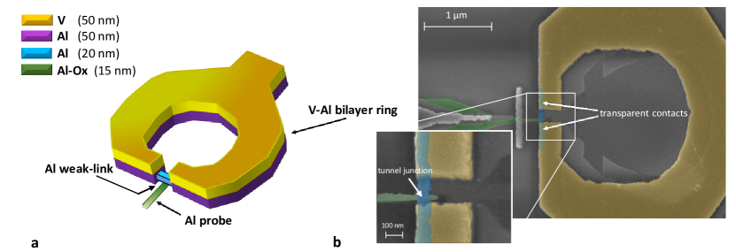
The SQUIPT concept design [see Figure 1(a)] is based on an Al nanowire embedded in a thick V-Al bilayer ring. Furthermore, an Al probe electrode is tunnel-coupled to the Al wire. The V layer deposited on top of the Al ring allows to increase the size of the minigap induced in the nanowire DOS, without compromising the junction quality. The Al layer was first deposited to insure the quality of the interface between the wire and the ring. The loop geometry of the superconducting electrode makes it possible to change the phase difference across the superconducting wire by applying an external magnetic field, due to the flux quantization. The choice of a thick layer for the superconducting ring is a necessary condition: i) to reduce the inverse proximity effect of the Al wire on the bilayer ring and ii) to decrease its normal-state resistance, and thus its kinetic inductance, thereby allowing a good phase biasing of the weak-link.
Interferometers are realized by electron-beam lithography (EBL) combined with three-angle shadow-mask evaporation (see Methods). Figure 1(b) shows a false-color scanning electron micrograph (SEM) of a typical V-based SQUIPT with a magnification of the weak-link zone. A crucial step in the processing is the vanadium deposition. Electron-beam evaporation of a refractory superconductor material such as V requires some special considerations. If no precautions are taken, the heating of the substrate damages the resist layer with the consequent metal-pattern deterioration. In this regard, Table I lists the characteristic parameters for all samples and demonstrates the excellent reproducibility achieved as a consequence of the fabrication process optimization.
Transport spectroscopy
The SQUIPT operation relies on the magnetic-flux control of the weak-link DOS. For ideal wire/ring interfaces, the minigap in the middle of the wire in the short junction limit, i.e., when the interelectrode spacing is shorter than the diffusive coherence length , is . Here, is the reduced Planck constant, is the diffusion coefficient of the nanowire, and is the energy gap of the ring. In the limit of negligible geometric and kinetic inductance of the ring compared to the weak-link kinetic inductance, the fluxoid quantization imposes where is the external magnetic flux piercing the loop.
As a result, the electric transport through the leads is -periodic with the flux of the applied magnetic field. Thus the SQUIPT acts as an interferometer. All the measurements are performed in a 3He/4He dilution refrigerator. The evolution of the electrical transport through the devices with the magnetic field is periodic with a period of G. The corresponding area for magnetic field penetration is , consistent with the size of the devices.
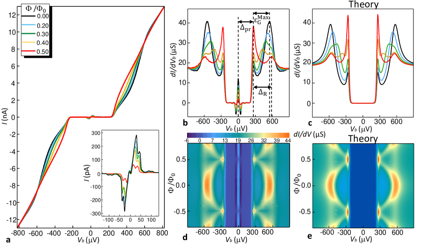
The characterization of the device (sample-A) at base temperature 25 mK is displayed in Fig.2. Figure 2(a) shows the characteristics of the device measured for different values of the applied magnetic flux. Here we can identify four regions: i) : the current is strongly suppressed and the phase modulation is negligible. ii) : the current increases significantly and a modulation with respect to the applied magnetic field is clearly visible. iii) : a crossing point of the current-voltage characteristics and a small modulation is still visible. iv) at higher voltage the curves approach the ohmic behaviour. Moreover, since the probe is superconducting, the tunnel junction supports a supercurrent, due to the Josephson effect. This is shown in the inset of Figure 2(a), where a magnification at low voltage is displayed. The supercurrent is pA at where the minigap is maximum, while its value is reduced down to pA at , showing a suppression with respect to the zero-flux value of the supercurrent. This behaviour gives an additional demonstration of the weak-link strong modulation of the minigap[23].
The magnetic field modulation of the nanowire DOS it is better visualized by considering the evolution of the differential conductance in the flux, as displayed in Figure 2(b). The curves are obtained through numerical differentiation of the current-voltage characteristic shown in panel (a). Following to the I-V characteristics, the conductance is strongly suppressed for , except for the structures related to the Josephson effect. At an abrupt increase in the current [see Figure 2a] results in a conductance peak, whose intensity is enhanced by the applied magnetic flux. At higher absolute voltage values the peak evolution is more complex. At zero flux additional conductance peaks are visible at . By increasing the magnetic flux, these peaks move toward smaller absolute voltages and their intensities become smaller, revealing the presence of additional structures at .
We explain this behaviour as follows. For simplicity, we consider only the quasiparticle contribution to the electrical current. The current through the probe/weak-link tunnel junction is given by[35]
| (1) |
where is the electron charge, is the normal-state resistance of the junction, is the quasiparticle energy with respect to the chemical potential and is the voltage across the junction. Here and are the normalized DOS functions of the probe and the nanowire, respectively. Since , we approximate , in order to simplify the calculation (see Supplementary Information). The system is assumed to be at thermal equilibrium at temperature , thus the states population is expressed by the Fermi-Dirac distribution . The superconducting probe DOS is , where is the BCS DOS, smeared by a finite Dynes parameter [36]. The nanowire DOS is affected by the proximity effect, which is properly described by the quasiclassical Usadel equations for diffusive systems[13, 38]. In the short junction limit the solution for the DOS can be obtained analytically [39]
| (2) |
where the ring is modeled as an effective BCS superconductor with pairing potential and Dynes parameter . This expression simplifies in the limit of a perfectly centered probe (), namely , where is the flux-dependent minigap induced in the nanowire DOS. Similar applies at , where the wire DOS is independent on the probing position . Notably, even for , the DOS retains a non-trivial dependence on the energy if .
Despite its simplicity, the model captures the main features observed in the differential conductance curves, including the evolution of the various peaks. The parameters of the model can be separately estimated thanks to the rich structure expressed by the experimental curves. The normal state resistance of the tunnel junction is easily extracted from the characteristic in the ohmic limit (where ) as . In the region the conductance is strongly suppressed due to the superconducting energy gap in the probe DOS, whereas at higher voltages the conductance is large. This feature allows us to estimate both the Al probe pairing potential and the ring Dynes parameter . Consequently, the Al probe Dynes parameter is determined from the small subgap conductance . The peaks at voltage which are visible at allows for an estimation of the bilayer effective pairing potential . Furthermore, it reveals a decentering in the probe position, which is set to , and is consistent with the scanning electron micrograph displayed in the enlarged view of the weak-link of Fig. 1 b). Summarizing, the three peaks structure at increasing voltage reside approximately at , where is the flux-dependent minigap induced in the nanowire DOS.
The theoretical curves for the differential conductance obtained using the above parameters are shown in Figure 2(c). An extended comparison is presented in Figures 2 (d)-(e), where the color plots of the experimental and theoretical differential conductance are displayed, respectively. Note that the maximum minigap value is slightly smaller than the ring pairing potential , namely . This can be related to nonidealities in the interface between the ring/weak-link contacts.
Two facts deserve discussion. First, it is difficult to give a precise estimate of the suppression of the minigap in the nanowire DOS at due to the presence of the probe pairing potential, which masks any possible small contribution around . Anyway, the strong flux-modulation of the tunnel probe supercurrent and the good agreement with the short-limit junction model confirm an almost full closure of the minigap. We also note that the incomplete suppression of the Josephson current at could stem from the decentering of probe junction. Despite this inconvenience, the choice of a superconducting probe is beneficial for improved magnetic sensor performance, as already shown in Al-based SQUIPTs [24, 23]. Second, the large broadening parameter for the ring DOS must be regarded as an effective parameter in this simplified description. In particular the origin of such large conductance is likely related to the presence of vanadium. Similar high subgap conductances have been observed in several occasions in V-based tunnel junctions[40, 18, 42, 11, 44], as well as in Nb-based tunnel junctions[45].
Magnetic sensing performance
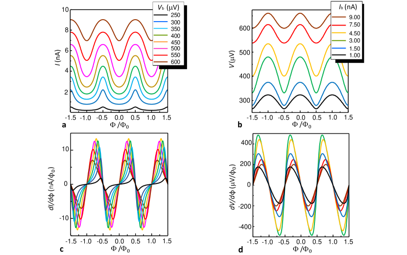
Here we investigate the interferometric behaviour of the sample-A SQUIPT at base temperature . For this purpose, we consider either the current modulation at fixed bias voltage and the voltage modulation at given input current . The results are reported in Figure 3.
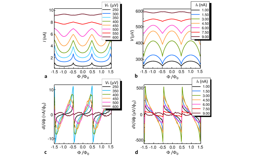
Panel 3(a) shows the current for several values of in the range from 250 V to 600 V, where the modulation is stronger. In accordance with the curves displayed in Figure 2(a), the shape of and the size of the modulation strongly depend on the bias voltage . The maximum current modulation in a period is approximately equal to around V. Note the change of concavity, i.e. the current decreases for increasing magnetic field in the range ] ( is an integer number), when exceeds the crossing point of the current-voltage characteristic [see Figure 2(a)].
In this configuration, the SQUIPT acts as a flux-to-current transducer. An important figure of merit for magnetic field sensing applications is the flux-to-current transfer function, namely . The curves obtained by numerical differentiation of the experimental data shown in Figure 3(a) for six different values of bias voltage around the optimum working point are shown in 3(c). The transfer function exhibits the maximum value of nA/ at . A similar analysis is repeated for the current bias configuration. Figures 3(b) and 3(d) show the voltage modulation and the flux-to-voltage transfer function for some values of the bias current in the range [1 nA,9 nA], respectively. In the half period [0,0.5] the voltage diminishes with the magnetic field due to the shrinking of the energy gap in the nanowire DOS, except for currents bigger than 8 nA, where the opposite occurs. The maximum voltage modulation and the maximum flux-to-voltage transfer function is obtained at 3.0 nA and reaches values as high as and , respectively.
Another relevant figure of merit for a magnetometer is the noise-equivalent flux (NEF) or flux sensitivity (), which gives the amount of noise per output bandwidth, and it is commonly expressed in units . Thanks to the intermediate value of the tunnel junction resistance, the devices can efficiently operate either with voltage amplification under DC current bias or with current amplification under DC voltage bias.
In the bias current configuration the flux sensitivity is expressed by where is the voltage noise spectral density. The intrinsic noise in the device is mainly given by the shot noise in the probe junction and it is expressed in the zero temperature limit by where is the differential resistance at the operating point. The extrinsic noise is the input-referred noise power spectral density of the preamplifier used in this setup (NF Corporation model LI-75A, with ). At the optimal bias point , and the intrinsic and extrinsic noises give approximately the same contributions, reading and , respectively.
Improved performances are obtained in the voltage bias configuration, where the intrinsic noise is reduced to , where . In this configuration, the extrinsic contribution of the current preamplifier (DL Instruments model 1211, with current spectral density noise ) can be disregarded. In both configurations, the quantum limited noise is negligible for typical ring geometric inductances .
.
Impact of the bath temperature
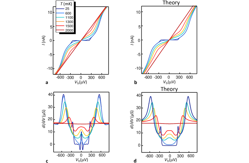
The role of the temperature is summarized in Figure 4. Panel 4(a) shows the current-voltage characteristics at several bath temperatures for (i.e., when the induced minigap is maximum). The corresponding theoretical curves are displayed in Figure 4(b) for the parameters extracted from the base temperature characterization, and assuming a pure BCS dependence both for and . As expected, the current increases with the temperature due to the broadening of the Fermi distributions and the shrinking of the probe and the ring superconducting pairing potentials (hence the reduction of the minigap in the nanowire DOS ). Furthermore, the nonlinear behaviour of the curves progressively decreases with the increase of the temperature, showing an almost linear characteristic around , when the superconducting features disappear. This value is consistent with the critical temperature extracted from the ring pairing potential , namely .
A deeper insight comes from the analysis of the differential conductances. Figure 4(c) shows the curves obtained by numerical differentiation of the experimental data, while the corresponding theoretical curves are plotted in Figure 4(d). Compared to the previously discussed features [see Figures 2(b) and 2(c)], the peak structures have an easier identification, since the probe position has no effect on the nanowire density of states at , i.e., . At low temperature, i.e. for the Josephson supercurrent contribution appears as a low voltage peak. By increasing the temperature, this contribution becomes small due to the reduction of the probe and ring pairing potentials. In addition, it is masked by the quasiparticle contribution at low voltage, which becomes significant due to Fermi distribution broadening, thence it is spotted already at .
The peaks at are smoothed out by the thermal broadening already at mK, where only the peaks at higher absolute voltage are detectable. As discussed before, the size of the minigap is related to the position of these peaks, which reside at . As expected, their intensity decreases by increasing the temperature and they shift toward smaller absolute voltages, confirming the shrinking of the minigap, especially above , according to the usual BCS dependence of the superconducting pairing potential. When the temperature reaches the K, the differential conductance becomes almost flat.
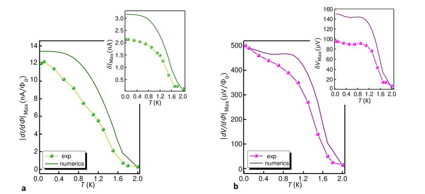
The temperature evolution of the interferometric performance of the device is shown in Figure 5. We already discussed how temperature increases the quasiparticle current, due to the thermal broadening and the shrinking of the probe and the ring gap. This smearing unavoidably influences the magnetic flux dependence of the current at fixed voltage and reduces the SQUIPT performance. This aspect is shown in Figure 5(a), where the maximum amplitude of the flux-to-current transfer function is displayed (points with line). This quantity decreases quite linearly with the temperature. Notably, the V-SQUIPT still exhibits a large sensitivity at 1.5 K. This represents a relevant improvement with respect to the previous SQUIPT devices, where similar values were only possible below K. In the inset, the maximum current modulation at fixed voltage is plotted against temperature, showing a swing pA at 1.5 K. Similar considerations apply for the maximum flux-to-voltage and maximum voltage modulation at fixed current bias. The results are reported in Fig. 5(b). These curves decrease slowly for temperatures K and then drop when the temperature approaches the bilayer critical temperature. As discussed before, the performances at 1.5 K are still remarkable, with a maximum transfer function and a maximum swing . In the plot the theoretical prediction, according to the simplified model used throughout the paper, are also reported (solid lines). The temperature evolution of the maximum flux-to-current (flux-to-voltage) transfer functions are similar to the experimental result, whereas significant deviations are observed in the current (voltage) swing. Our simplified model gives a somewhat less satisfactory fit for the current and voltage magnetic flux dependence than for the differential conductance (see Supplementary Information).
Discussion
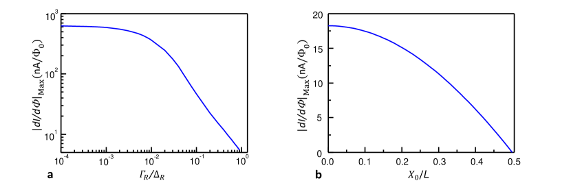
In summary, we have presented the fabrication and characterization of V-based SQUIPTs realized with a V-Al bilayer ring. Our quantum interference proximity transistors show good magnetometric performance with low noise-flux sensitivity down to at base temperature . Previously, higher interferometric performances have been reported for Al-based SQUIPTs (magnetic flux resolution as low as )[23]. From the theoretical side, the V-based SQUIPT should guarantee better performance compared to the Al-based technology, since the predicted flux-to-voltage transfer function scales as [21]. This is not observed due to the high subgap conductance of the superconducting vanadium, which limits the device performance. This is displayed in the first panel of Fig.6, where the theoretical maximum flux-to-current transfer function is plotted as a function of the ring Dynes parameter. A smaller role is played also by the decentering of the probe respect to the middle of the nanowire, as shown in Fig. 6(b). The origin of the large subgap conductance of vanadium is still not understood and may be related to the evaporation process. Despite this, the use of vanadium allows us to obtain unprecedented performances in terms of maximum operating temperature (), since the Al-based SQUIPTs typically work only up to 1 K. Furthermore, our interferometers still exhibit high sensitivity ( and ) at K. The main features in our devices are well reproduced within a simplified theoretical model. The V-based SQUIPT configuration is a proof-of-concept showing the V-Al material combination is an suitable candidate for the realization of high-performance magnetometers operating above K.
Finally, furthermore improvements will be possible with the adoption of superconducting materials with wider energy-gap, such as lead, niobium and niobium nitride. This will extend the magnetometer working operation at higher temperatures, allowing SQUIPT applications at temperatures accessible with the technology of 4He cryostats, in order to try to compete with the state of the art nanoSQUID[46, 47] (flux resolution ).
Methods
Device fabrication details
The devices were fabricated through single electron-beam lithography process followed by a three-angle shadow-mask evaporation of metals through a suspended resist mask. At first, an oxidized silicon wafer was covered with a suspended bilayer resist mask (1200-nm copolymer, 250-nm polymethyl methecrylate (PMMA)) by spin-coated process. Then the device structures have been patterned onto the substrate via electron-beam lithography. The EBL step is followed by development in 1:3 mixture of MIBK:IPA (methyl isobutyl ketone:isopropanol) for typically 1 min and 30 sec, followed by a rinse in pure IPA and drying with nitrogen. Then, the sample was processed in a ultra-high vacuum (UHV) evaporator (base pressure of ) for the metalization process. 15 nm of Al was deposited at 1.5Å/s at an angle of =40° to form the superconducting electrode of the probe tunnel junction. Subsequently, the sample was exposed to 100 mTorr for 5 min to realize the tunnel barrier. Next, the sample was tilted to an angle of =20° for the evaporation of 20 nm of Al to form the superconducting nanowire. Subsequently, 50 nm of Al was deposited at =0° to realize the first layer of the bilayer ring. Finally, at the same angle 50 nm of V was evaporated at 3Å/s in order to realize the upper layer of V/Al superconducting ring. The magneto-electric measurements were performed in a 3He/4He dilution refrigerator in a range temperature from 25 mK to 2 K using room-temperature preamplifiers.
References
- [1] Sohn, L., Kouwenhoven, L. & Schön, G. Mesoscopic Electron Transport. Nato Science Series E: (Springer Netherlands, 1997).
- [2] Clarke, J. & Braginski, A. The SQUID Handbook: Fundamentals and Technology of SQUIDs and SQUID Systems (Wiley, 2004).
- [3] Giazotto, F. et al. Opportunities for mesoscopics in thermometry and refrigeration: Physics and applications. Rev. Mod. Phys. 78, 217–274 (2006).
- [4] Giazotto, F. & Martinez-Perez, M. J. The Josephson heat interferometer. Nature 492, 401–405 (2012).
- [5] Solinas, P., Gasparinetti, S., Golubev, D. & Giazotto, F. A Josephson radiation comb generator. Scientific Reports 5, 12260 (2015).
- [6] Pekola, J. P. et al. Hybrid single-electron transistor as a source of quantized electric current. Nat. Phys. 4, 120–124 (2008).
- [7] Clarke, J. & Wilhelm, F. K. Superconducting quantum bits. Nature 453, 1031 (2008).
- [8] You, J. Q. & Nori, F. Atomic physics and quantum optics using superconducting circuits. Nature 474, 589–597 (2011).
- [9] Vasyukov, D. et al. A scanning superconducting quantum interference device with single electron spin sensitivity. Nat. Nanotech. 8, 639 (2013).
- [10] Fornieri, A., Timossi, G., Bosisio, R., Solinas, P. & Giazotto, F. Negative differential thermal conductance and heat amplification in superconducting hybrid devices. Phys. Rev. B 93, 134508 (2016).
- [11] Paolucci, F., Marchegiani, G., Strambini, E. & Giazotto, F. Phase-Coherent temperature amplifier. ArXiv e-prints(2016) arxiv:1612.00170.
- [12] Govenius, J., Lake, R. E., Tan, K. Y. & Möttönen, M. Detection of zeptojoule microwave pulses using electrothermal feedback in proximity-induced Josephson junctions. Phys. Rev. Lett. 117, 030802 (2016).
- [13] Giazotto, F., Peltonen, J. T., Meschke, M. & Pekola, J. P. Superconducting quantum interference proximity transistor. Nat. Phys. 6, 254 (2010).
- [14] Jabdaraghi, R. N., Meschke, M. & Pekola, J. P. Non-hysteretic superconducting quantum interference proximity transistor with enhanced responsivity. Applied Physics Letters 104, 082601 (2014).
- [15] Tinkham, M. Introduction to Superconductivity: Second Edition (Wiley-VCH, 2004).
- [16] De Gennes, P. G. Superconductivity Of Metals And Alloys (Addison-Wesley Publishing Company, 1966).
- [17] Buzdin, A. I. Proximity effects in superconductor-ferromagnet heterostructures. Rev. Mod. Phys. 77, 935–976 (2005).
- [18] Kim, J. et al. Visualization of geometric influences on proximity effects in heterogeneous superconductor thin films. Nat. Phys. 8, 464–469 (2012).
- [19] le Sueur, H., Joyez, P., Pothier, H., Urbina, C. & Esteve, D. Phase controlled superconducting proximity effect probed by tunneling spectroscopy. Phys. Rev. Lett. 100, 197002 (2008).
- [20] Hammer, J. C., Cuevas, J. C., Bergeret, F. S. & Belzig, W. Density of states and supercurrent in diffusive SNS junctions: Roles of nonideal interfaces and spin-flip scattering. Phys. Rev. B 76, 064514 (2007).
- [21] Virtanen, P., Ronzani, A. & Giazotto, F. Spectral characteristics of a fully-superconducting Squipt. Phys. Rev. Applied 6, 054002 (2016).
- [22] Ronzani, A., D’Ambrosio, S., Virtanen, P., Giazotto, F. & Altimiras, C. Phase-driven collapse of the Cooper condensate in a nanosized superconductor. ArXiv e-prints(2016) arxiv:1611.06263.
- [23] Ronzani, A., Altimiras, C. & Giazotto, F. Highly sensitive superconducting quantum-interference proximity transistor. Phys. Rev. Applied 2, 024005 (2014).
- [24] D’Ambrosio, S., Meissner, M., Blanc, C., Ronzani, A. & Giazotto, F. Normal metal tunnel junction-based superconducting quantum interference proximity transistor. Applied Physics Letters 107, 113110 (2015).
- [25] Samaddar, S. et al. Niobium-based superconducting nano-device fabrication using all-metal suspended masks. Nanotechnology 24, 375304 (2013).
- [26] Jabdaraghi, R. N., Peltonen, J. T., Saira, O.-P. & Pekola, J. P. Low-temperature characterization of Nb-Cu-Nb weak links with Ar ion-cleaned interfaces. Applied Physics Letters 108, 042604 (2016).
- [27] García, C. P. & Giazotto, F. Josephson current in nanofabricated V/Cu/V mesoscopic junctions. Appl. Phys. Lett. 94, 132508 (2009).
- [28] Ronzani, A., Baillergeau, M., Altimiras, C. & Giazotto, F. Micro-superconducting quantum interference devices based on V/Cu/V Josephson nanojunctions. Applied Physics Letters 103, 052603 (2013).
- [29] Quaranta, O., Spathis, P., Beltram, F. & Giazotto, F. Cooling electrons from 1 to 0.4 k with redV-based nanorefrigerators. Applied Physics Letters 98, 032501 (2011).
- [30] Spathis, P. et al. Hybrid redInAs nanowire–vanadium proximity SQUID. Nanotechnology 22, 105201 (2011).
- [31] Giazotto, F. & Taddei, F. Hybrid superconducting quantum magnetometer. Phys. Rev. B 84, 214502 (2011).
- [32] Annunziata, A. J. et al. Tunable superconducting nanoinductors. Nanotechnology 21, 445202 (2010).
- [33] Luomahaara, J., Vesterinen, V., Grönberg, L. & Hassel, J. Kinetic inductance magnetometer. Nature Communications 4872 (2014).
- [34] McCaughan, A. N., Zhao, Q. & Berggren, K. K. NanoSQUID operation using kinetic rather than magnetic induction. Scientific Reports 28095 (2016).
- [35] Barone, A. & Paternò, G. Physics and applications of the Josephson effect (Wiley, 1982).
- [36] Dynes, R. C., Garno, J. P., Hertel, G. B. & Orlando, T. P. Tunneling study of superconductivity near the metal-insulator transition. Phys. Rev. Lett. 53, 2437–2440 (1984).
- [37] Usadel, K. D. Generalized diffusion equation for superconducting alloys. Phys. Rev. Lett. 25, 507–509 (1970).
- [38] Belzig, W., Wilhelm, F. K., Bruder, C., Schön, G. & Zaikin, A. D. Quasiclassical Green’s function approach to mesoscopic superconductivity. Superlattices and Microstructures 25, 1251 – 1288 (1999).
- [39] Heikkilä, T. T., Särkkä, J. & Wilhelm, F. K. Supercurrent-carrying density of states in diffusive mesoscopic josephson weak links. Phys. Rev. B 66, 184513 (2002).
- [40] Seifarth, H. & Rentsch, W. V–VxOy–Pb Josephson tunnel junctions of high stability. Physica status solidi (a) 18, 135–146 (1973).
- [41] Noer, R. J. Superconductive tunneling in vanadium with gaseous impurities. Phys. Rev. B 12, 4882–4885 (1975).
- [42] Dettmann, F., Blüthner, K., Pertsch, P., Weber, P. & Albrecht, G. A study of V-VOx-Pb Josephson tunnel junctions. physica status solidi (a) 44, 577–584 (1977).
- [43] Gibson, G. A. & Meservey, R. Evidence for spin fluctuations in vanadium from a tunneling study of Fermi-liquid effects. Phys. Rev. B 40, 8705–8713 (1989).
- [44] Shimada, H., Miyawaki, K., Hagiwara, A., Takeda, K. & Mizugaki, Y. Characterization of superconducting single-electron transistors with small Al/AlOx /V Josephson junctions. Superconductor Science and Technology 27, 115015 (2014).
- [45] Julin, J. K. & Maasilta, I. J. Applications and non-idealities of submicron Al–AlOx–Nb tunnel junctions. Superconductor Science and Technology 29, 105003 (2016).
- [46] Granata, C. & Vettoliere, A. Nano superconducting quantum interference device: A powerful tool for nanoscale investigations. Physics Report 614, 1 – 69 (2016).
- [47] Schmelz, M. et al. Nearly quantum limited nanoSQUIDs based on cross-type Nb/AlOx/Nb junctions. Superconductor Science and Technology 30, 014001 (2017).
Acknowledgments
The authors thank F. Paolucci, E. Enrico, and A. Fornieri for fruitful discussions. The MIUR-FIRB2013 – Project Coca (Grant No. RBFR1379UX) and the European Research Council under the European Union’s Seventh Framework Program (FP7/2007-2013)/ERC Grant agreement No. 615187- COMANCHE are acknowledged for partial financial support. The work of E.S. is funded by a Marie Curie Individual Fellowship (MSCA-IFEF-ST No. 660532-SuperMag).
Author contribution statement
F.G. conceived the experiment. N.L. fabricated the samples. N.L., G.M. and E.S. performed the measurements. G.M. and P.V. developed the theoretical model. N.L and G.M analyzed the data. N.L. and G.M. wrote the manuscript. All authors reviewed the manuscript.
Additional Information
The authors declare no competing financial interests.
Supplementary Information: High operating temperature in V-based superconducting quantum interference proximity transistors.
Nadia Ligato, Giampiero Marchegiani, Pauli Virtanen, Elia Strambini, Francesco Giazotto
Kinetic Inductance for the ring and the wire of the SQUIPT
Within the Mattis-Bardeen theory[2], the kinetic inductance of a superconducting strip with length , width and thickness is given by , where is the superconducting order parameter and is the normal state resistance of the superconducting strip (here is the normal state resistivity). This expression can be used to estimate the kinetic inductance of the superconducting loop of the SQUIPT when the ring consist of a single superconductor.
For a comparison, we consider a sinusoidal current-phase relation for the superconducting weak-link, which in the short junction limit is valid when the temperature is not too small compared to the critical temperature[3]. Under this assumption, the minimal kinetic inductance at zero phase bias reads , where is the normal state resistance of the weak link.
The ratio between the kinetic inductance of the wire and the ring is
| (S1) |
where the superscripts NW, R refer to the nanowire and ring, respectively.
The dimensions of the Al nanowire (device A) are nm, nm and nm. We assume , which is the typical resistivity for 25 nm Al layer at 4.2 K evaporated in past experiments, consistently with the values reported in the literature[4, 5, 6, 7]. If we consider a ring made of Al with dimensions m, nm and m and same resistivity (although in general the resistivity drops by increasing the thickness of the layer) we obtain .

The resistivity of the vanadium may vary quite strongly depending on evaporation conditions. Considering literature values [8, 9, 10, 11, 12], we estimate the V layer resistivity to range approximately from the same resistivity of the Al to a value 5 times larger . As a consequence, this would produce a potentially large deviation from the ideal condition .
When the superconducting ring is made of a bilayer, the situation is more involved (as we detail in the next subsection): In first approximation it is possible to model the total kinetic inductance of the bilayer as the parallel of the kinetic inductance of the two layers. This simple calculation shows how the inclusion of the Al underlayer provides a suitable geometry for the good phase biasing of the device, independently of the specific properties of the vanadium layer.
Bilayer modeling
The spectral properties of the V-Al bilayer in the dirty limit can be modeled within the Usadel formalism[13]. The problem formulation is similar to the one given by Fominov and Feigel’man for the properties of a thin NS bilayer[14]. In the numerical computation we model the bilayer as a superconducting strip with total thickness nm and we assume a ratio 1:1 ( nm) between the two layers, accordingly to the experimental realization (Fig. 1). We assume a clean interface between the two layers.
A parameter relevant for the properties for the bilayer is
| (S2) |
where and are the normal state resistances and the diffusion constants of the materials Al,V (Einstein relation is assumed and is the density of states at the Fermi level). The coupling constants in the two superconducting layers depend in the weak coupling limit on the cutoff energy where is the Debye temperature.
The density of states at the Fermi level are taken from the literature. Here is the density of states at the Fermi level for atom ( , )[15], is the mass density ( , ) [16] and is the atomic mass ( , ) [17]. The Debye temperature is assumed to be the same for both materials K.
For the Al layer we choose a critical temperature equal to the bulk value K, corresponding to a zero temperature order parameter eV, and typical resistivity and Dynes parameter obtained through electron beam evaporation.
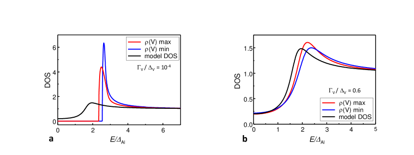
As already stated before, the properties of the vanadium deposited through electron beam evaporation are extremely sensitive to the evaporation conditions. In accordance with the discussion in the previous section, we consider and as minimal and maximal resistivity in the numerical computation. Similarly apply to the critical temperature of the vanadium, which can be significantly smaller than the bulk value[18], depending on the evaporation rate. In our numerical computation we set K, which is reasonable due to the low evaporation rate and previous realizations [19]. Finally we consider two cases for the Dynes parameter of vanadium: a very ideal situation and an extremely leaking layer . The latter seems to describe better the results of our experiment as we show in Fig.2, where the DOS at the bottom of the Al layer is compared to the effective BCS DOS used in the main text. In particular the resistivity of the Vanadium plays a role in the determination of the energy gap of the bilayer, but does not affect significantly the subgap density of states. In particular, the large subgap conductance observe in the experiment must be associated to an high effective Dynes parameter in the V layer even in this model. Notably, the results compare quite well with the effective BCS model used in the main text.
In this model, the kinetic inductance of the bilayer is evaluated as , where the supercurrent dispersion is computed starting from the solution of the Usadel equation. An approximate expression for ultrathin layers[14] can be obtained in the Cooper limit[20], where the superconducting energy gap is homogeneous along the bilayerṪhe kinetic inductance of the ring is therefore given by the parallel of the kinetic inductances of the two layers:
| (S3) |
In Tab. 1, we see how the approximate expressions for the kinetic inductance compare to the values obtained through the rigorous calculation. Generally, the approximation underestimates the kinetic inductance somewhat, and does not take nonzero Dynes parameters into account.
| cm) | (pH) | (pH) | |
|---|---|---|---|
| 10-4 | 5 | 1.36 | 1.31 |
| 10-4 | 25 | 2.54 | 2.19 |
| 0.6 | 5 | 2.06 | 1.31 |
| 0.6 | 25 | 3.67 | 2.19 |
Impact of the finite width of the probe
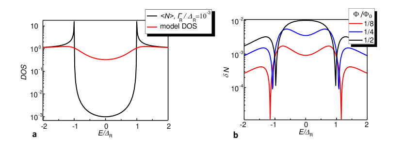
In the main text is stated that, in order to simplify the calculation, we disregard the finite width of the probe. First, we show that the high subgap conductance observed in the differential conductance curves is not originated by the finite extension of the probe. In Fig. S3, panel a) we compare the effective DOS used in the main text with the DOS obtained after averaging over the probe width , where we set an ideal Dynes parameter . The subgap conductance in the latter case is too small to explain the experimental results. Then we quantify the relative deviation between the simplified expression and the integrated expression through the figure of merit
| (S4) |
In Fig.S3 panel b) we plot this function for different values of (there is no deviation at ). We see that the maximum relative deviation is always smaller or equal than 1.
Theoretical flux dependence
For completeness, in this section we discuss the theoretical flux dependence obtained from the theoretical model adopted throughout the main text. The plots corresponding to the panel of the Fig. 3 of the main text are displayed in Fig. S4 We note that the comparison with the experimental data is certainly less satisfactory compared to the differential conductance curves. In particular the predicted oscillation is larger than the observed (especially at larger voltages/currents) and the curves are quite smoother around . Notably, despite these deviations, the maximum current-to-flux and voltage-to-flux transfer functions are close to the one observed in the experiment. This plot explain why a large deviation in the temperature evolution of the swing is observed in the theoretical curves in Fig. 5 of the main text, whereas the temperature evolution of the maximum transfer function works better.
References
- [1] le Sueur, H., Joyez, P., Pothier, H., Urbina, C. & Esteve, D. Phase controlled superconducting proximity effect probed by tunneling spectroscopy. \JournalTitlePhys. Rev. Lett. 100, 197002 (2008).
- [2] Tinkham, M. Introduction to Superconductivity: Second Edition. Dover Books on Physics (Dover Publications, 2004).
- [3] Likharev, K. K. Superconducting weak links. \JournalTitleRev. Mod. Phys. 51, 101–159 (1979).
- [4] Ullom, J. N., Fisher, P. A. & Nahum, M. Measurements of quasiparticle thermalization in a normal metal. \JournalTitlePhys. Rev. B 61, 14839–14843 (2000).
- [5] Courtois, H., Meschke, M., Peltonen, J. T. & Pekola, J. P. Origin of hysteresis in a proximity josephson junction. \JournalTitlePhys. Rev. Lett. 101, 067002 (2008).
- [6] Hübler, F., Lemyre, J. C., Beckmann, D. & v. Löhneysen, H. Charge imbalance in superconductors in the low-temperature limit. \JournalTitlePhys. Rev. B 81, 184524 (2010).
- [7] Peltonen, J. T., Muhonen, J. T., Meschke, M., Kopnin, N. B. & Pekola, J. P. Magnetic-field-induced stabilization of nonequilibrium superconductivity in a normal-metal/insulator/superconductor junction. \JournalTitlePhys. Rev. B 84, 220502 (2011).
- [8] Teplov, A. A., Mikheeva, M. N., Golyanov, V. M. & Gusev, A. N. Superconducting transition temperature, critical magnetic fields, and the structure of vanadium films. \JournalTitleSov. Phys. Jetp. 44, 587 (1976).
- [9] Nicolet, M.-A. Diffusion barriers in thin films. \JournalTitleThin Solid Films 52, 415–443 (1978).
- [10] Kanoda, K., Mazaki, H., Hosoito, N. & Shinjo, T. Upper critical field of v-ag multilayered superconductors. \JournalTitlePhys. Rev. B 35, 6736–6748 (1987).
- [11] Gibson, G. A. & Meservey, R. Evidence for spin fluctuations in vanadium from a tunneling study of fermi-liquid effects. \JournalTitlePhys. Rev. B 40, 8705–8713 (1989).
- [12] Aarts, J., Geers, J. M. E., Brück, E., Golubov, A. A. & Coehoorn, R. Interface transparency of superconductor/ferromagnetic multilayers. \JournalTitlePhys. Rev. B 56, 2779–2787 (1997).
- [13] Usadel, K. D. Generalized diffusion equation for superconducting alloys. \JournalTitlePhys. Rev. Lett. 25, 507–509 (1970).
- [14] Fominov, Y. V. & Feigel’man, M. V. Superconductive properties of thin dirty superconductor-normal-metal bilayers. \JournalTitlePhys. Rev. B 63, 094518 (2001).
- [15] McMillan, W. L. Transition temperature of strong-coupled superconductors. \JournalTitlePhys. Rev. 167, 331–344 (1968).
- [16] Haynes, W. CRC Handbook of Chemistry and Physics, 97th Edition (CRC Press, 2016).
- [17] Meija, J. et al. Atomic weights of the elements 2013 (IUPAC technical report). \JournalTitlePure and Applied Chemistry 88 (2016).
- [18] Noer, R. J. Superconductive tunneling in vanadium with gaseous impurities. \JournalTitlePhys. Rev. B 12, 4882–4885 (1975).
- [19] Quaranta, O., Spathis, P., Beltram, F. & Giazotto, F. Cooling electrons from 1 to 0.4 k with v-based nanorefrigerators. \JournalTitleApplied Physics Letters 98, 032501 (2011).
- [20] Cooper, L. N. Superconductivity in the neighborhood of metallic contacts. \JournalTitlePhys. Rev. Lett. 6, 689–690 (1961).