Local optical control of ferromagnetism and chemical potential in a topological insulator
Abstract
Many proposed experiments involving topological insulators (TIs) require spatial control over time-reversal symmetry and chemical potential. We demonstrate reconfigurable micron-scale optical control of both magnetization (which breaks time-reversal symmetry) and chemical potential in ferromagnetic thin films of Cr-(Bi,Sb)2Te3 grown on SrTiO3. By optically modulating the coercivity of the films, we write and erase arbitrary patterns in their remanent magnetization, which we then image with Kerr microscopy. Additionally, by optically manipulating a space charge layer in the underlying SrTiO3 substrates, we control the local chemical potential of the films. This optical gating effect allows us to write and erase p-n junctions in the films, which we study with photocurrent microscopy. Both effects are persistent and may be patterned and imaged independently on a few-micron scale. Dynamic optical control over both magnetization and chemical potential of a TI may be useful in efforts to understand and control the edge states predicted at magnetic domain walls in quantum anomalous Hall insulators.
I Introduction
The unusual topology of electronic bands in some materials can produce quantum states that are stabilized by symmetry. Topological insulators (TIs) have attracted particular attention for their symmetry-protected surface and edge states, which may hold promise for applications in spintronics and quantum computing Hasan and Kane (2010); Qi and Zhang (2011). Ferromagnetic TIs combine a topologically-nontrivial band structure with ferromagnetism, which intrinsically breaks time-reversal symmetry (TRS), and therefore may produce unusual electromagnetic phenomena such as the topological magnetoelectric effect Qi et al. (2008); Essin et al. (2009), quantized Kerr and Faraday rotation Tse and MacDonald (2010); Wu et al. (2016), and quantization of the anomalous Hall effect (QAHE) Yu et al. (2010); Chang et al. (2013). However, while the quantum states in an ideal TI are protected by symmetry, most topologically-nontrivial materials have proven difficult to grow and engineer. In particular, residual bulk conductivity, and the tendency of TI materials to degrade during semiconductor processing, have impeded many experimental efforts Kong et al. (2011); Benia et al. (2011); Wang et al. (2012). Harnessing the unique physics of these materials will require better understanding and control of their magnetism and disorder, as well as methods to engineer TI devices without degrading the properties that make these materials unique.
A major challenge in TI research is to identify systems in which the energies and symmetries of TI physics can be reliably controlled in the laboratory. For instance, a criterion for the QAH insulator state is for the chemical potential of electrons to lie within an energy gap in the surface state dispersion, where , is the local magnetization, and is the surface normal Hasan and Kane (2010); Qi and Zhang (2011). At the edges of a uniformly magnetized film, the top and bottom surfaces meet and therefore changes sign, causing to vanish. In sufficiently thin films, the vanishing gap produces 1D conductive states that propagate along the edges of the film, and their quantized conductance is observed as the QAHE Yu et al. (2010); Chang et al. (2013). Similar edge states are predicted to occur along magnetic domain walls, where the direction of magnetization inverts. These domain wall-bound states are of considerable present interest Wickles and Belzig (2012); Feng et al. (2015); Wang et al. (2015a, b); Liu et al. (2016), but they have not yet been observed directly. Methods to intentionally pattern the magnetization and chemical potential of TI materials in situ during experiments may be particularly useful in efforts to detect, and eventually to harness, these unique phenomena.
Much research has focused on understanding and minimizing the sources of both magnetic Okada et al. (2011); Wang et al. (2015c); Lachman et al. (2015); Wang et al. (2016) and chemical potential Roushan et al. (2009); Beidenkopf et al. (2011); Kastl et al. (2015) disorder in TI materials. However, relatively few techniques have been explored to systematically control these parameters. Magnetic control of TI materials has focused largely on introducing TRS-breaking in different layers along the growth axis of thin films by modulation doping of magnetic ions Mogi et al. (2015), or in magnetic-nonmagnetic bilayer devices Kou et al. (2013a). Individual magnetic dopants have also been arranged on TI surfaces with STM techniques Schlenk et al. (2013).
Spatial control of chemical potential in TI materials is difficult due to material degradation during top gate fabrication and other cleanroom processes Kong et al. (2011); Benia et al. (2011); Wang et al. (2012). Previously, we reported an all-optical technique to tune the chemical potential of a variety of ultra-thin materials grown on SrTiO3 Yeats et al. (2015). By optically manipulating space-charge in the underlying substrate, we created an effective local back-gate that was strong enough to create p-n junctions in non-magnetic thin films of (Bi,Sb)2Te3. These features were persistent and optically erasable, allowing arbitrary spatial control of the chemical potential without additional materials or fabrication.
In this article, we demonstrate persistent, reconfigurable optical control over both the electron chemical potential and local magnetization of ferromagnetic thin films of Cr-(Bi,Sb)2Te3 grown on SrTiO3. First, we use simultaneous magneto-optical Kerr effect (MOKE) and anomalous Hall effect (AHE) measurements to establish a correspondence between optical and electrical measures of TI magnetism. We image the dynamics of magnetic coercion in the films using scanning Kerr microscopy, which suggest the presence of a nano-scale domain structure. We also employ both optical and electrostatic gating techniques to characterize both carrier-mediated and van Vleck-mediated ferromagnetism in the films. Finally, we demonstrate the ability to optically pattern and reconfigure the local chemical potential and local magnetization of the films using a two-color optical and magneto-optical recording protocol. We characterize these coexisting patterns with simultaneous scanning Kerr and photocurrent microscopies, showing that independent spatial control of both chemical potential and magnetization can be achieved at the same time in a ferromagnetic TI on a few-micron scale.
II Methods
Samples consisted of 5-10 quintuple-layer (QL) films of Crx(BiySb1-y)2-xTe3 grown by molecular beam epitaxy (MBE) on (111)-oriented SrTiO3. Growth parameters and detailed material characterization data are presented in a separate manuscript Richardella et al. (2015a). The composition of the films is comparable to previous materials grown in the same MBE chamber that showed QAHE at very low temperatures ( K) Liu et al. (2016); Lachman et al. (2015); Kandala et al. (2015). For consistency, we present data in the main text from one representative sample, a 9 QL film of Cr0.15(Bi0.5,Sb0.5)1.85Te3 capped with a 4.5 nm layer of Al. Other films are discussed in the supplementary materials. Hall bars were patterned in all films by mechanically scratching away the growth layer with a needle, thereby avoiding sample contamination from lithographic processes. The samples were mounted in an optical cryostat and an electromagnet was used to apply an out-of-plane magnetic field at the sample.
The local magnetization of the film was imaged with scanning Kerr microscopy in the polar MOKE geometry. A beam of linearly polarized light was directed at normal incidence onto the sample and the rotation in polarization of the reflected beam was measured using lock-in techniques as described in the supplementary materials. A reflective microscope objective was used to avoid unwanted Faraday rotation from glass optics Kondo et al. (2012). Illumination was provided by a HeNe laser, with a photon energy ( 1.96 eV) in the vicinity of a known resonance in the MOKE spectrum of similar materials Patankar et al. (2015). For simultaneous resistance, AHE, and MOKE hysteresis measurements, the laser spot was positioned on an unconnected leg of the Hall bar to avoid optical effects on the transport measurements.
Resistance measurements were performed using standard AC lock-in techniques with an excitation current of 100 nA and a reference frequency of 17 Hz. Electrical contacts to all samples were made with indium and were ohmic. The chemical potential of the films was tuned by applying a voltage to the back-side of the substrate, or through a persistent, substrate-based optical gating effect Yeats et al. (2015). A fiber-coupled ultraviolet (UV, 370 nm) light emitting diode (LED) was used to provide illumination for optical gating. For simultaneous Kerr and photocurrent imaging, a virtual null current preamplifier was used to measure the photocurrent induced by the MOKE laser spot as it was rastered across the sample.
III Results and Discussion
We used simultaneous magneto-optical and magneto-transport measurements to characterize the ferromagnetism of thin films of Cr-(Bi,Sb)2Te3 at 2.9 K. Fig. 1(a) shows the evolution of polar Kerr angle and anomalous Hall resistance in a representative 9 QL film of Cr-(Bi,Sb)2Te3 as a function of increasing and decreasing magnetic field. Clear, roughly square-shaped hysteresis is visible in both MOKE and AHE traces, indicative of ferromagnetic ordering with an easy axis out of the sample plane. We estimate the film has a Curie temperature K (see supplementary materials). Fig. 1(b) shows the measurement geometry. Fig. 1(c) shows the longitudinal resistance as a function of applied field at 2.9 K. The peaks at have been observed in similar materials and are attributed to increased scattering from magnetic disorder during coercion Checkelsky et al. (2012). Although similarly-composed materials grown in the same MBE chamber have shown quantized conductance at K Kandala et al. (2015); Lachman et al. (2015); Liu et al. (2016), the absolute resistance values we observe indicate that conductivity is dominated by surface- and bulk-conductive channels (as opposed to quantized edge states) at the temperatures achievable in our optical cryostat ( K).
Optical illumination during MOKE experiments could affect the magnetism of the films. Fig. 1(d) shows the coercive field extracted from MOKE hysteresis measurements as a function of laser power at 3.2 K and with a spot size of 1 µ m . The coercivity of the film decreases with illumination, fitting well to a power law relation (dashed line) from 20 µ W to 2 mW, where local heating is likely to dominate. The trend plateaus at low powers, showing good agreement with the coercivity extracted from AHE hysteresis in the absence of illumination (red arrow). This suggests that illumination from MOKE measurements conducted below 2 µ W are unlikely to significantly affect the magnetic properties of the film.

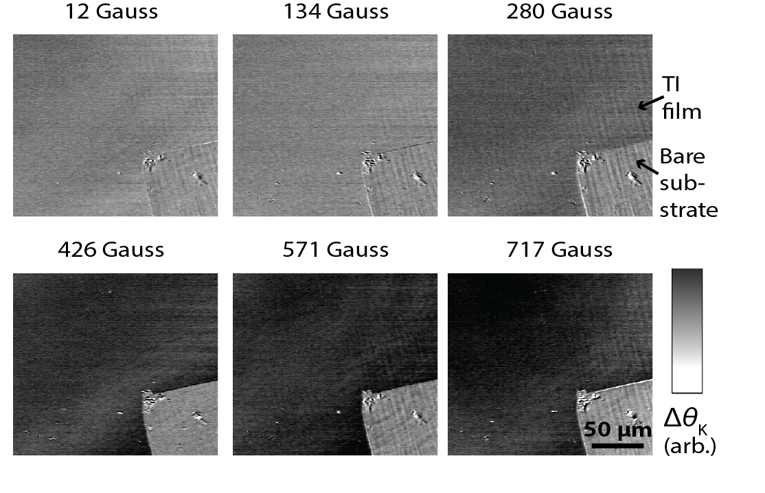
By rastering the MOKE laser spot across the sample at low power, it is straightforward to produce spatial images of the magnetization of the films. Fig. 2 shows scanning Kerr micrographs of the reversal of remanent magnetization in a thin film of Cr-(Bi,Sb)2Te3 after 5-s exposures to successively larger fields. The images show a continuous and spatially-uniform change in remanent magnetization. This is most likely an indication that magnetic inversion occurs on length scales smaller than the resolving power of our apparatus ( 1 µ m ). This is consistent with the sub-micron size domains observed by Lachman et al. by scanning nano-SQUID microscopy in similar materials Lachman et al. (2015). We see similar behavior in all of the films grown on SrTiO3. By contrast, we observe inversion by domain-wall motion on longer length scales in one very heavily Cr-doped film grown on InP (see supplementary materials). However, this heavily-doped sample is unlikely to exhibit QAHE.
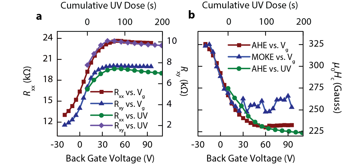
Field-effect gating is generally needed to position the chemical potential within the surface state gap in QAHE studies Chang et al. (2013). We used electrostatic back-gating, as well as a substrate-based persistent optical gating effect, to characterize the response of the film to the field effect. UV illumination produces a persistent field effect in thin films grown on SrTiO3 via electrical polarization of the underlying substrate, and this effect is functionally equivalent to a an electrostatic back-gate Yeats et al. (2015). Fig. 3(a) shows the evolution of and as a function of either (bottom axis), or previous exposure to UV illumination (top axis). The resistances evolve similarly with either type of gating. The response is consistent with expectations for an initially p-type film that is gated just past its Dirac point to a weakly n-type regime at V or 60 s of cumulative UV exposure. Because the optical gating effect is persistent, all measurements were performed in the dark 60 s after each exposure in order to avoid any transient effects from illumination of the sample.
Carrier-independent magnetism is important for magnetic TIs to achieve the QAHE because magnetization must remain after tuning the chemical potential to the surface-state energy gap Yu et al. (2010). While carrier-mediated magnetism dominates in the more lightly Cr-doped films we have studied (see supplementary information), in the present film we observe magnetism that is largely independent of gate-tuning by either optical or electrostatic effects. Fig. 3(b) shows the evolution of (extracted from simultaneous AHE and MOKE measurements) as a function of electrostatic back-gating (bottom axis) or previous exposure to UV light (top axis). decreases by with increasing (or previous exposure to UV light), consistent with only partially hole-mediated ferromagnetism. This is consistent with other reports of coexisting hole-mediated and van Vleck-mediated ferromagnetism in moderately Cr-doped (Bi,Sb)2Te3 Kou et al. (2013b); Richardella et al. (2015b). Notably, the values of extracted from AHE and MOKE measurements correspond well in the absence of a gate effect, but at higher voltages (or UV exposures), MOKE hysteresis measurements indicate a larger than AHE hysteresis measurements. This may imply that optically-excited carriers from MOKE measurements can play a role in the carrier-mediated ferromagnetism of these materials, and this contribution is relatively more important when free holes are otherwise depleted by a back-gate.
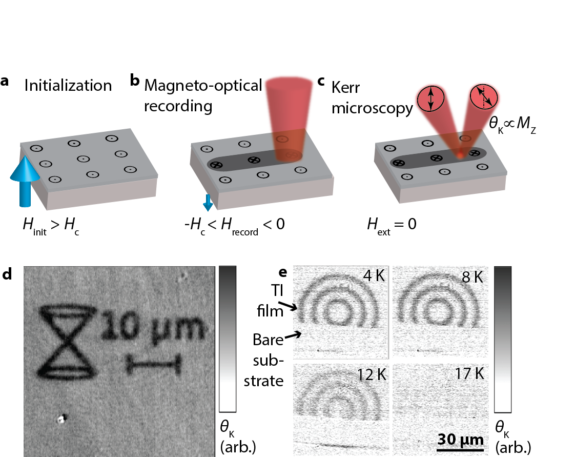
Many proposed applications of magnetic TI materials require spatial control of TRS-breaking. Fig. 4(a-c) shows a protocol for magneto-optical recording Chen et al. (1968) in Cr-(Bi,Sb)2Te3. After initialization with a field , a high-intensity laser spot is used to locally reduce the coercivity of the film, such that a weak external field will invert the magnetization of the film only in the illuminated area. When the laser and field are shut off, the magnetic pattern remains, and can be imaged with low-power scanning Kerr microscopy. Figure 4(d) shows a Kerr micrograph of intentionally-patterned magnetization in Cr-(Bi,Sb)2Te3. The minimum feature size is µ m . We find that magnetic patterns remain persistent 24 h unless they are erased with a coercive magnetic field or by raising the temperature above . After erasure, no signs of the old pattern appear in subsequent Kerr images, and new patterns may be recorded. Fig. 4(e) shows magneto-optical recording as a function of temperature, indicating that the effect vanishes above . Moreover, patterns were written across the edge of the film, and no patterning effect was observed on the bare substrate area. The lack of response in these areas rules out other explanations due to effects in the substrate, such as optical polarization of magnetic impurities Rice et al. (2014).
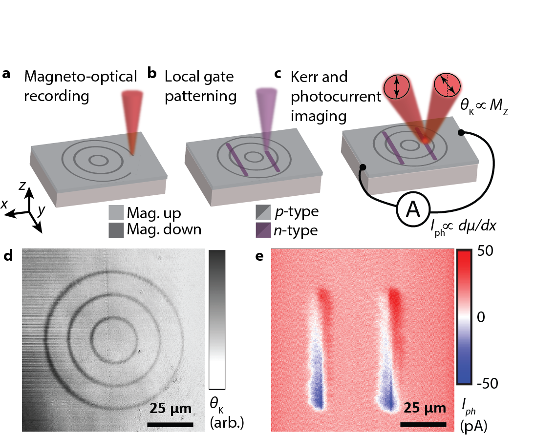
In addition to controlling the local magnetization through magneto-optical recording, simultaneous patterning of the local chemical potential can be achieved by confining the substrate-based optical gating effect to a focused spot. Fig. 5(a-c) shows a schematic of the patterning technique. First, magneto-optical recording is performed as described above to write three concentric circles in the local magnetization of the film. Then, two rectangular regions are exposed to UV light, which creates an effective local back-gate, raising the chemical potential of the film in those areas, and causing them to become n-type. Scanning Kerr (Fig. 5(d)) and photocurrent (Fig. 5(e)) microscopies are then performed simultaneously using the same focused laser spot, as described in the methods. These images provide a map of the local magnetization and chemical potential gradient of the film, respectively. The photocurrent micrograph is consistent with the presence of local n-type regions in the otherwise p-type film. The image axes and pattern are tilted slightly with respect to the path between electrodes. The Kerr micrograph indicates that the magnetic pattern has survived the optical gating process, highlighting the presence of carrier-independent ferromagnetism in these films, and the ability of the films to support persistent, micron-scale magnetic features regardless of carrier density.
Once written, both magnetic and chemical potential patterns persist indefinitely on accessible laboratory timescales. However, a relatively high laser power (30 µ W ) is needed to produce clear photocurrent images, and so the imaging process relaxes the UV gating effect Yeats et al. (2015). Repeated imaging can therefore be used to erase the field of view. The elevated laser power during magneto-optical recording may also relax the optical gating effect, and so magnetic recording must be performed as the first step in the process. Despite the elevated power during photocurrent imaging, the magnetic patterns do not appear to degrade so long as the external field is held at zero. Within these constraints, we find that magneto-optical recording and UV gate patterning combine well without noticeable cross-talk in the Kerr and photocurrent images. The combination of these two effects therefore allows independent, reconfigurable optical control of both the local magnetization (TRS-breaking) and chemical potential of a magnetic TI material on a few-micron scale.
IV Summary and Outlook
We have reported a set of optical measurement and control protocols, which we use to study and manipulate the local magnetization and chemical potential of thin films of Cr-(Bi,Sb)2Te3 grown on SrTiO3. In the low-power measurement regime, we show a close correspondence between MOKE and AHE measurements of magnetic hysteresis in the films, suggesting that polarization-resolved optical techniques complement electrical measurements in understanding the magnetic properties of TI films. We use scanning Kerr microscopy to image magnetic inversion in the films, suggesting the presence of a nano-scale domain structure. Furthermore, we use both MOKE and AHE measurements to investigate the partially carrier-mediated ferromagnetism of the films, which we then control either with an electrostatic back-gate or a persistent optical gating effect. Finally by employing various scanning optical microscopy techniques, we demonstrate simultaneous local control of both the local chemical potential and local magnetization of the films. We show that both properties can be arbitrarily patterned, reconfigured, and imaged independently on a few-micron scale.
Because the magnetization direction determines the sign of the surface state energy gap , the ability to control the magnetization of a Cr-(Bi,Sb)2Te3 film at the micron scale may have immediate applications in efforts to detect the 1D edge states predicted to occur in TIs at magnetic domain wall boundaries Hasan and Kane (2010); Qi and Zhang (2011); Wickles and Belzig (2012). Although the films we measure do not reach the QAH regime at 3 K, our approach is equally applicable in lower-temperature environments. Improvements in growth protocols, such as modulation doping of magnetic impurities Mogi et al. (2015), may also bring QAH physics to the K regime. Freedom to write and modify arbitrarily complicated magnetization patterns in situ may be especially useful for prototyping devices based on TI physics, such as spin filters Hammer and Pötz (2013) and spin-based transistors Hammer et al. (2013). The magnetic patterning and microscopy techniques we present may also be useful in testing theoretical predictions about the mutual interactions between magnetic domain wall motion and spin-torque from TI surface states Tserkovnyak and Loss (2012); Ferreiros and Cortijo (2014). Since both optical effects are persistent and bidirectional, a series of incremental recording steps may allow regions of a particular magnetization or chemical potential to be moved in two dimensions without changing topology. This might have relevance for studying solid state analogies to particle physics and related proposals for quantum information processing Das Sarma et al. (2005); Nayak et al. (2008); Ferreira and Loss (2013).
V Acknowledgments
We thank J. van Bree for useful discussions. We acknowledge use of the NSF National Nanofabrication Users Network Facility at Penn State. This work is supported by the Office of Naval Research (grants N00014-15-1-2369 and N00014-15-1-2370), the Air Force Office of Scientific Research Multidisciplinary University Research Initiative (grant FA9550-14-1-0231), the NSF Materials Research Science and Engineering Centers (grant NSF-DMR-1420709), and the National Science Foundation (grants NSF-DMR-1306300 and NSF-DMR-1306510). This study is based in part upon research conducted at The Pennsylvania State University Two-Dimensional Crystal Consortium – Materials Innovation Platform (2DCC-MIP) which is supported by NSF cooperative agreement DMR-1539916. This material is based upon work supported by Laboratory Directed Research and Development (LDRD) funding from Argonne National Laboratory, provided by the Director, Office of Science, of the U.S. Department of Energy under Contract No. DE-AC02-06CH11357.
References
- Hasan and Kane (2010) M. Z. Hasan and C. L. Kane, Colloquium: Topological insulators, Rev. Mod. Phys. 82, 3045 (2010).
- Qi and Zhang (2011) X.-L. Qi and S.-C. Zhang, Topological insulators and superconductors, Rev. Mod. Phys. 83, 1057 (2011).
- Qi et al. (2008) X.-L. Qi, T. L. Hughes, and S.-C. Zhang, Topological field theory of time-reversal invariant insulators, Phys. Rev. B 78, 195424 (2008).
- Essin et al. (2009) A. M. Essin, J. E. Moore, and D. Vanderbilt, Magnetoelectric polarizability and axion electrodynamics in crystalline insulators, Phys. Rev. Lett. 102, 146805 (2009).
- Tse and MacDonald (2010) W. K. Tse and A. H. MacDonald, Giant magneto-optical kerr effect and universal faraday effect in thin-film topological insulators, Phys. Rev. Lett. 105, 1 (2010).
- Wu et al. (2016) L. Wu, M. Salehi, N. Koirala, J. Moon, S. Oh, and N. P. Armitage, Quantized Faraday and Kerr rotation and axion electrodynamics of a 3D topological insulator, Science 354, 1124 (2016).
- Yu et al. (2010) R. Yu, W. Zhang, H.-J. Zhang, S.-C. Zhang, X. Dai, and Z. Fang, Quantized anomalous Hall effect in magnetic topological insulators. Science 329, 61 (2010).
- Chang et al. (2013) C.-Z. Chang, J. Zhang, X. Feng, J. Shen, Z. Zhang, M. Guo, K. Li, Y. Ou, P. Wei, L.-L. Wang, Z.-Q. Ji, Y. Feng, S. Ji, X. Chen, J. Jia, X. Dai, Z. Fang, S.-C. Zhang, K. He, Y. Wang, L. Lu, X.-C. Ma, and Q.-K. Xue, Experimental observation of the quantum anomalous Hall effect in a magnetic topological insulator. Science 340, 167 (2013).
- Kong et al. (2011) D. Kong, J. J. Cha, K. Lai, H. Peng, J. G. Analytis, S. Meister, Y. Chen, H. J. Zhang, I. R. Fisher, Z. X. Shen, and Y. Cui, Rapid surface oxidation as a source of surface degradation factor for Bi2Se3, ACS Nano 5, 4698 (2011).
- Benia et al. (2011) H. M. Benia, C. Lin, K. Kern, and C. R. Ast, Reactive chemical doping of the Bi2Se3 topological insulator, Phys. Rev. Lett. 107, 177602 (2011).
- Wang et al. (2012) X. Wang, G. Bian, T. Miller, and T. C. Chiang, Fragility of surface states and robustness of topological order in Bi 2Se 3 against oxidation, Phys. Rev. Lett. 108, 1 (2012).
- Wickles and Belzig (2012) C. Wickles and W. Belzig, Reflectionless transport of surface Dirac fermions on topological insulators with induced ferromagnetic domain walls, Phys. Rev. B 86, 035151 (2012).
- Feng et al. (2015) Y. Feng, X. Feng, Y. Ou, J. Wang, C. Liu, L. Zhang, D. Zhao, G. Jiang, S.-C. Zhang, K. He, X. Ma, Q.-K. Xue, and Y. Wang, Observation of the Zero Hall Plateau in a Quantum Anomalous Hall Insulator, Phys. Rev. Lett. 115, 126801 (2015).
- Wang et al. (2015a) Y. H. Wang, J. R. Kirtley, F. Katmis, P. Jarillo-Herrero, J. S. Moodera, and K. A. Moler, Observation of chiral currents at the magnetic domain boundary of a topological insulator, Science 349, 948 (2015a).
- Wang et al. (2015b) Y. H. Wang, J. R. Kirtley, F. Katmis, P. Jarillo-Herrero, J. S. Moodera, and K. A. Moler, Retraction, Science 350, 1482 (2015b).
- Liu et al. (2016) M. Liu, W. Wang, A. R. Richardella, A. Kandala, J. Li, A. Yazdani, N. Samarth, and N. P. Ong, Large discrete jumps observed in the transition between Chern states in a ferromagnetic Topological Insulator, Sci. Adv. 2, e1600167 (2016).
- Okada et al. (2011) Y. Okada, C. Dhital, W. Zhou, E. D. Huemiller, H. Lin, S. Basak, A. Bansil, Y.-B. Huang, H. Ding, Z. Wang, S. D. Wilson, and V. Madhavan, Direct Observation of Broken Time-Reversal Symmetry on the Surface of a Magnetically Doped Topological Insulator, Phys. Rev. Lett. 106, 206805 (2011).
- Wang et al. (2015c) W. Wang, F. Yang, C. Gao, J. Jia, G. D. Gu, and W. Wu, Visualizing ferromagnetic domains in magnetic topological insulators, APL Mater. 3, 083301 (2015c).
- Lachman et al. (2015) E. O. Lachman, A. F. Young, A. Richardella, J. Cuppens, H. R. Naren, Y. Anahory, A. Y. Meltzer, A. Kandala, S. Kempinger, Y. Myasoedov, M. E. Huber, N. Samarth, and E. Zeldov, Visualization of superparamagnetic dynamics in magnetic topological insulators, Sci. Adv. 1, e1500740 (2015).
- Wang et al. (2016) W. Wang, C.-Z. Chang, J. S. Moodera, and W. Wu, Visualizing ferromagnetic domain behavior of magnetic topological insulator thin films, npj Quantum Mater. 1, 16023 (2016).
- Roushan et al. (2009) P. Roushan, J. Seo, C. V. Parker, Y. S. Hor, D. Hsieh, D. Qian, A. Richardella, M. Z. Hasan, R. J. Cava, and A. Yazdani, Topological surface states protected from backscattering by chiral spin texture. Nature 460, 1106 (2009).
- Beidenkopf et al. (2011) H. Beidenkopf, P. Roushan, J. Seo, L. Gorman, I. Drozdov, Y. S. Hor, R. J. Cava, and A. Yazdani, Spatial fluctuations of helical Dirac fermions on the surface of topological insulators, Nat. Phys. 7, 939 (2011).
- Kastl et al. (2015) C. Kastl, P. Seifert, X. He, K. Wu, Y. Li, and A. Holleitner, Chemical potential fluctuations in topological insulator (Bi 0.5 Sb 0.5 ) 2 Te 3 -films visualized by photocurrent spectroscopy, 2D Mater. 2, 024012 (2015).
- Mogi et al. (2015) M. Mogi, R. Yoshimi, A. Tsukazaki, K. Yasuda, Y. Kozuka, K. S. Takahashi, M. Kawasaki, and Y. Tokura, Magnetic modulation doping in topological insulators toward higher-temperature quantum anomalous Hall effect, Appl. Phys. Lett. 107, 182401 (2015).
- Kou et al. (2013a) X. Kou, L. He, M. Lang, Y. Fan, K. Wong, Y. Jiang, T. Nie, W. Jiang, P. Upadhyaya, Z. Xing, Y. Wang, F. Xiu, R. N. Schwartz, and K. L. Wang, Manipulating surface-related ferromagnetism in modulation-doped topological insulators. Nano Lett. 13, 4587 (2013a).
- Schlenk et al. (2013) T. Schlenk, M. Bianchi, M. Koleini, A. Eich, O. Pietzsch, T. O. Wehling, T. Frauenheim, A. Balatsky, J.-L. Mi, B. B. Iversen, J. Wiebe, A. A. Khajetoorians, P. Hofmann, and R. Wiesendanger, Controllable magnetic doping of the surface state of a topological insulator, Phys. Rev. Lett. 110, 126804 (2013).
- Yeats et al. (2015) A. L. Yeats, Y. Pan, A. Richardella, P. J. Mintun, N. Samarth, and D. D. Awschalom, Persistent optical gating of a topological insulator, Sci. Adv. 1, e1500640 (2015).
- Richardella et al. (2015a) A. Richardella, A. Kandala, J. S. Lee, and N. Samarth, Characterizing the structure of topological insulator thin films, APL Mater. 3, 083303 (2015a).
- Kandala et al. (2015) A. Kandala, A. Richardella, S. Kempinger, C.-X. Liu, and N. Samarth, Giant anisotropic magnetoresistance in a quantum anomalous Hall insulator, Nat. Commun. 6, 7434 (2015).
- Kondo et al. (2012) Y. Kondo, Y. Nakamura, K. Yamakawa, S. Ishio, and J. Ariake, Development of microscopic magnetometer with reflective objective using magneto-optical Kerr effect, J. Appl. Phys. 111, 1 (2012).
- Patankar et al. (2015) S. Patankar, J. P. Hinton, J. Griesmar, J. Orenstein, J. S. Dodge, X. Kou, L. Pan, K. L. Wang, A. J. Bestwick, E. J. Fox, D. Goldhaber-Gordon, J. Wang, and S.-C. Zhang, Resonant magneto-optic Kerr effect in the magnetic topological insulator Cr(SbxBi1-x)2Te3, Phys. Rev. B 92, 214440 (2015).
- Checkelsky et al. (2012) J. G. Checkelsky, J. Ye, Y. Onose, Y. Iwasa, and Y. Tokura, Dirac-fermion-mediated ferromagnetism in a topological insulator, Nat. Phys. 8, 729 (2012).
- Kou et al. (2013b) X. Kou, M. Lang, Y. Fan, Y. Jiang, T. Nie, J. Zhang, W. Jiang, Y. Wang, Y. Yao, L. He, and K. L. Wang, Interplay between Different Magnetisms in Cr-Doped Topological Insulators. ACS Nano 7, 9205 (2013b).
- Richardella et al. (2015b) A. Richardella, A. Kandala, and N. Samarth, Topological Insulator Thin Films and Heterostructures: Epitaxial Growth, Transport, and Magnetism, in Topological Insulators: Fundamentals and Perspectives, edited by F. Ortmann, S. Roche, and S. O. Valenzuela (Wiley-VCH Verlag GmbH & Co. KGaA, Weinheim, Germany, 2015) pp. 295–329.
- Chen et al. (1968) D. Chen, J. F. Ready, and E. Bernal G., MnBi Thin Films: Physical Properties and Memory Applications, J. Appl. Phys. 39, 3916 (1968).
- Rice et al. (2014) W. D. Rice, P. Ambwani, M. Bombeck, J. D. Thompson, G. Haugstad, C. Leighton, and S. A. Crooker, Persistent optically induced magnetism in oxygen-deficient strontium titanate. Nat. Mater. 13, 481 (2014).
- Hammer and Pötz (2013) R. Hammer and W. Pötz, Dynamics of domain-wall Dirac fermions on a topological insulator: A chiral fermion beam splitter, Phys. Rev. B 88, 235119 (2013).
- Hammer et al. (2013) R. Hammer, C. Ertler, and W. Pötz, Solitonic Dirac fermion wave guide networks on topological insulator surfaces, Appl. Phys. Lett. 102, 193514 (2013).
- Tserkovnyak and Loss (2012) Y. Tserkovnyak and D. Loss, Thin-film magnetization dynamics on the surface of a topological insulator, Phys. Rev. Lett. 108 (2012).
- Ferreiros and Cortijo (2014) Y. Ferreiros and A. Cortijo, Domain wall motion in junctions of thin-film magnets and topological insulators, Phys. Rev. B 89, 024413 (2014).
- Das Sarma et al. (2005) S. Das Sarma, M. Freedman, and C. Nayak, Topologically Protected Qubits from a Possible Non-Abelian Fractional Quantum Hall State, Phys. Rev. Lett. 94, 166802 (2005).
- Nayak et al. (2008) C. Nayak, S. H. Simon, A. Stern, M. Freedman, and S. Das Sarma, Non-Abelian anyons and topological quantum computation, Rev. Mod. Phys. 80, 1083 (2008).
- Ferreira and Loss (2013) G. J. Ferreira and D. Loss, Magnetically Defined Qubits on 3D Topological Insulators, Phys. Rev. Lett. 111, 106802 (2013).