Thickness dependence and dimensionality effects of charge and magnetic orderings in \ceLa1/3Sr2/3FeO3 thin films
Abstract
We investigate the thickness effects on charge and magnetic orderings in Fe perovskite oxide \ceLa_1/3Sr_2/3FeO3/\ceSrTiO3 thin films by hard x-ray and resonant soft x-ray scattering (RSXS) with changing thin film thickness systematically. We found that the correlation lengths of the magnetic ordering along the in-plane and out-of-plane directions are comparable and proportional to the thickness, and shows stronger thickness dependence than those of charge orderg. The magnetic ordered states disappear when the correlation length of magnetic ordering decreases to that of charge ordering through the intrinsic thickness effects. Surface sensitive grazing-incident RSXS revealed that the orderings exist even in the surface region, which indicates that the observed orderings is not affected by surface effect like oxygen vacancies. Critical thickness is in 5-15 nm, which corresponds to 4-11 antiferromagnetic ordering period. This critical value seems to be common to other ferromagnetic oxide thin films.
Charge, spin, and orbital orderings in 3d transition metal perovskite oxides closely relate to the origin of remarkable physics phenomena such as metal-insulator transition, superconductivity and giant magnetoresistance.Imada, Fujimori, and Tokura (1998); Tokura and Nagaosa (2000) For instance, stripe structures of spin and charge ordering in superconducting cuprates were reported Tranquada et al. (1995); Tranquada (1998) and the charge density wave was found to compete with superconducting state.Ghiringhelli et al. (2012); Blanco-Canosa et al. (2013); He et al. (2016)
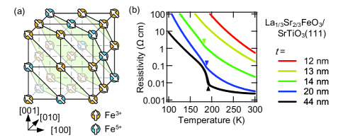
One of such 3d transition-metal oxides, \ceLa1/3Sr2/3FeO3 attracts much attention due to its unusual high valence state and charge disproportionation. Mössbauer spectroscopy showed charge disproportionation of 3\ceFe^3.67+2\ceFe^3++\ceFe^5+ accompanied by an antiferromagnetic ordering at critical temperature .Takano and Takeda (1983); Battle, Gibb, and Nixon (1988) Electronic conductivity shows a transition associated with the charge disproportionation transition at .Takano and Takeda (1983) Neutron scattering study revealed that charge and magnetic orderings exist along the [111] direction and Fe layers stack in the sequence of \ceFe^3+ ^-Fe^5+ ^-Fe^3+ ^-Fe^3+ v -Fe^5+ v -Fe^3+ v as shown in Fig. 1(a).Battle, Gibb, and Lightfoot (1990) Electron diffraction demonstrated structural distortion along the direction.Li et al. (1997) This stacking layer structure is also supported by the exchange interaction determined by inelastic neutron scattering McQueeney et al. (2007) and Hartree-Fock calculation.Mizokawa and Fujimori (1998) As for the electronic structure, x-ray absorption spectroscopy of Fe 2p 3d and O 1s 2p suggests that holes induced by Sr doping exhibits O 2p hole character.Abbate et al. (1992) The unusually high valence states \ceFe^4+ and \ceFe^5+ are expressed rather as \ce3d^5L and \ce3d^5L^2, where \ceL represents an O 2p hole.Abbate et al. (1992); Bocquet et al. (1992); Imada, Fujimori, and Tokura (1998)
The charge ordering exists even in thin films.Wadati et al. (2005); Okamoto et al. (2010); Ueno et al. (2006); Sichel-Tissot et al. (2013); Xie et al. (2014) This is considered to be due to the small lattice distortion accompanied by the charge disproportionation in contrast to the case of \ceFe^4+ oxide \ceCaFeO3 Matsuno et al. (2004) or Mn perovskite oxides such as and .Tokura (2006) For this reason, \ceLa1/3Sr2/3FeO3 thin film is a suitable material for extracting intrinsic effects of thickness and dimensionality on electronic states without the influence of lattice distortion. However, there have been no studies of thickness effect except for resistivity measurements.Minohara et al. (2016); Devlin et al. (2014) Minohara et al. studied the precise thickness dependence of resistivity in \ceLa1/3Sr2/3FeO3/\ceSrTiO3 thin films and found that the ordered states were suppressed with thickness below 14 nm as shown by curves in Fig. 1(b).Minohara et al. (2016) Resistivity becomes too high to determine the resistivity jump with decreasing thickness due to the insulating \ceSrTiO3 substrates and resistivity is not a direct evidence for the orderings. Therefore, x-ray is a suitable technique for obtaining a detailed view of and determining the existence of the orderings in \ceLa1/3Sr2/3FeO3thin films.
Okamoto et al. performed hard x-ray scattering for charge ordering and resonant soft x-ray scattering (RSXS) for magnetic ordering at the Fe absorption.Okamoto et al. (2010) One cannot observe the magnetic ordering peak by hard x-ray Okamoto et al. (2010) due to the small cross section of magnetic scattering.Blume (1985) RSXS is a suitable technique to study magnetic orderings in thin films and small crystals.Blume (1985); Okamoto et al. (2010); Fink et al. (2013); Matsuda et al. (2015); Wadati et al. (2012); Huang et al. (2006); Wadati et al. (2014); Ghiringhelli et al. (2012); Blanco-Canosa et al. (2013); He et al. (2016); Yamasaki et al. (2016) We obtained a strong sensitivity of magnetic scattering at the Fe absorption edge due to strong spin-orbit coupling of Fe core levels. In addition to reflection geometry RSXS, we performed grazing-incident RSXS (GI-RSXS). When the incident angle is below the total reflection angle, the probing depth of x-ray becomes small and one can access surface-sensitive information. This technique was used to study surface states of ordering and revealed that surface melting in \ceLa_0.5Sr_1.5MnO_4 Wakabayashi et al. (2007); Wilkins et al. (2011) and surface orbital ordering in \ceLaCoO3 thin film.Yamasaki et al. (2016)
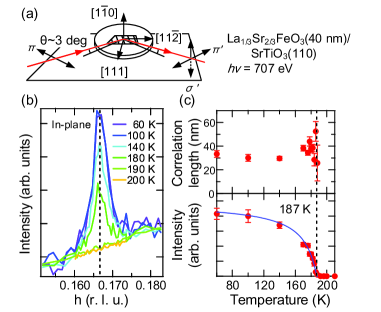
The \ceLa1/3Sr2/3FeO3 thin films were grown on \ceSrTiO3(111) and (110) substrates by pulsed laser deposition method. The details of the sample fabrication were described elsewhere.Minohara et al. (2016) The thickness of the thin films was determined from the Laue fringes around the (111) Bragg peaks (not shown). We performed hard x-ray scattering experiments for \ceLa_1/3Sr_2/3FeO3(t = 5, 15, 17 and 78 nm)/SrTiO3(111) thin films at BL-4C of Photon Factory, KEK. We measured the charge ordering peak with hard x-ray. The experimental geometry is shown in Fig. 2(a). The incident photon energy of x-ray was 12.4 keV. Incident x-ray was -polarized and scattered x-ray was detected without polarization analysis and hence includes - and -polarized photons. We performed RSXS experiments for \ceLa_1/3Sr_2/3FeO3(t = 5, 17, 37 and 78 nm)/SrTiO3(111) thin films at the BL-19B of Photon Factory. We observed the magnetic ordering scattering peak by RSXS. The incident photon energy was 707 eV at the Fe absorption edge. Incident x-ray was -polarized and scattered photon was detected by an energy-resolved silicon drift detector without polarization analysis. We removed O fluorscence emission by tuning energy windows to the Fe L edge. The geometry is shown in Fig. 3(a). The sample was \ceLa_1/3Sr_2/3FeO3(40 nm)/SrTiO3(110), which has in-plane modulation vectors. In order to investigate the surface states, we performed GI-RSXS in the geometry shown in Fig. 4(a) using the sample \ceLa_1/3Sr_2/3FeO3(40 nm)/SrTiO3(110), which has in-plane modulation vectors.
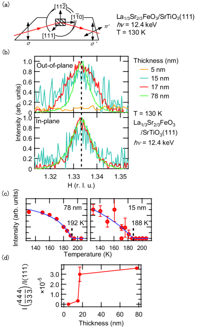
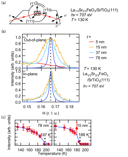
Figure 2(b) shows the charge ordering peak along the out-of-plane direction and along the in-plane direction. The charge orderings exist in , and disappears in . The peak width shows little dependence on thickness. Figure 2(c) shows the temperature dependence of the peak intensity. The critical temperature was determined from this dependence. Figure 2(d) shows that the charge ordering peak intensity drops sharply when the thickness is reduced to 15 nm. This drop suggests that critical thickness exists and the value is , which is in good agreement with the previous electric resistivity study.Minohara et al. (2016) Figure 3(b) shows the magnetic ordering peak along both directions. The peak width increases when thickness becomes thinner and the peak disappears at . This disappearance is also consistent with the charge ordering behavior shown in Fig. 2(b, d). The correlation length is given as the inverse of the half width of half maximum, namely, . This peak width tendency of the magnetic ordering indicates that correlation length decreases when thickness becomes thinner. The critical temperature was also determined by the temperature dependence of the peak intensity as shown in Fig. 3(c). The correlation length and the critical temperature of the charge and magnetic ordered states are summarized in Fig. 5 and will be discussed later.
It may be the case that surface states differ from bulk states by possible oxygen vacancies due to the high valence state of \ceFe^3.67+. Effects of oxygen vacancy affects the orderings Sichel-Tissot et al. (2013); Xie et al. (2014) and probing surface state is important for studying the thickness dependence. We performed GI-RSXS study in order to investigate the surface states. We studied \ceLa_1/3Sr_2/3FeO3(40 nm)/\ceSrTiO3(110) thin film with the in-plane modulation vector and measured the magnetic orderings peak . Its probing depth was determined to be approximately 2 nm by calculation from x-ray absorption spectroscopy and the incident angle. Figure 4(b) shows the result of GI-RSXS and Fig. 4(c) shows the correlation length and the transition temperature. and the peak position of surface states are the same as those of bulk states shown in Fig. 5 and correlation length is in the same order of the results of the bulk state. These results indicate that the surface states of \ceLa1/3Sr2/3FeO3 thin films are the same as the bulk state and the measured thickness dependence is not due to the surface effects but due to intrinsic dimensionality effects.
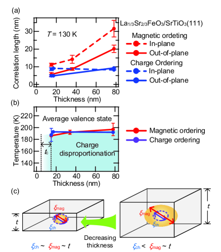
The obtained correlation length is plotted as a function of thickness in Fig. 5(a) at 130 K. Out-of-plane correlation length of magnetic orderings is proportional to the thickness. Geometrical limitation of thickness explains this behavior of the out-of-plane correlation length. However, the in-plane correlation length also decreases when the thickness of the thin film becomes thinner. This behavior suggests that magnetic orderings have an isotropic correlation. Comparing with correlation length of magnetic ordering , the thickness dependence of the correlation length of charge orderings is much weaker than that of magnetic orderings. When the thickness is sufficiently large (), the correlation length of magnetic ordering is in the same order of thickness (). When the thickness and reach at the thickness of approximately 15 nm (), the orderings disappear. This indicates that a minimal value of domain size of exists and thickness limitation makes the correlation length of magnetic ordering below the minimal value and suppresses the orderings. This behavior is schematically shown in Fig. 5(c). The obtained critical thickness of 5-15 nm corresponds to 4-11 units with the antiferromagnetic ordering period of 6 u. c. as a unit. This critical number of units seems to be common to other ferromagnetic perovskite oxide (3-8 units Huijben et al. (2008); Yoshimatsu et al. (2009)). We obtained the critical temperature from temperature dependence of scattering peak area intensity and it is plotted as a function of thickness as shown in Fig. 5(b). slightly decreased when thin film became thinner and of charge and magnetic orderings were almost the same. This slight decrease is consistent with other magnetic ordered compounds and matches the result of resistivity study.Minohara et al. (2016)
In summary, we performed hard x-ray scattering and RSXS experimets for the charge and magnetic orderings in \ceLa1/3Sr2/3FeO3/\ceSrTiO3 thin films with changing the thickness systematically. We also performed GI-RSXS experiment in order to investigate surface states of \ceLa1/3Sr2/3FeO3 thin films with the unusually high valence state. Magnetic ordering is stable even in the surface region in spite of its high valence states and this suggests that the thickness dependence comes from the intrinsic geometrical effects.The correlation length of the magnetic ordering is comparable and proportional to the thickness. Reduced thickness suppresses the ordered states at the critical temperature through this relationship between and . It will be interesting to study systematically thickness dependences of charge, magnetic or orbital orderings with x-ray scattering for various thin films and elucidate behaviors especially around critical thicknesses.
Acknowledgements.
X-ray scattering measurements were performed under the approval of the Photon Factory Program Advisory Committee (Proposals No. 2015G556, 2016PF-BL-19B, 2015S2-007) at the Institute of Material Structure Science, KEK. This work was partially supported by the Ministry of Education, Culture, Sports, Science and Technology of Japan (X-ray Free Electron Laser Priority Strategy Program). K. Y. acknowledges the support from ALPS program of the University of Tokyo.References
- Imada, Fujimori, and Tokura (1998) M. Imada, A. Fujimori, and Y. Tokura, Rev. Mod. Phys. 70, 1039 (1998).
- Tokura and Nagaosa (2000) Y. Tokura and N. Nagaosa, Science 288, 462 (2000).
- Tranquada et al. (1995) J. M. Tranquada, B. J. Sternlieb, J. D. Axe, Y. Nakamura, and S. Uchida, Nature 375, 561 (1995).
- Tranquada (1998) J. M. Tranquada, J. Phys. Chem. Solids 59, 2150 (1998).
- Ghiringhelli et al. (2012) G. Ghiringhelli, M. Le Tacon, M. Minola, S. Blanco-Canosa, C. Mazzoli, N. B. Brookes, G. M. De Luca, A. Frano, D. G. Hawthorn, F. He, T. Loew, M. M. Sala, D. C. Peets, M. Salluzzo, E. Schierle, R. Sutarto, G. A. Sawatzky, E. Weschke, B. Keimer, and L. Braicovich, Science 337, 821 (2012).
- Blanco-Canosa et al. (2013) S. Blanco-Canosa, A. Frano, T. Loew, Y. Lu, J. Porras, G. Ghiringhelli, M. Minola, C. Mazzoli, L. Braicovich, E. Schierle, E. Weschke, M. Le Tacon, and B. Keimer, Phys. Rev. Lett. 110, 187001 (2013).
- He et al. (2016) J. He, P. Shafer, T. R. Mion, V. T. Tra, Q. He, J. Kong, Y.-D. Chuang, W. L. Yang, M. J. Graf, J.-Y. Lin, Y.-H. Chu, E. Arenholz, and R.-H. He, Nat. Commun. 7, 10852 (2016).
- Takano and Takeda (1983) M. Takano and Y. Takeda, Bull. Inst. Chem. Res., Kyoto Univ. 61, 406 (1983).
- Battle, Gibb, and Nixon (1988) P. Battle, T. Gibb, and S. Nixon, J. Solid State Chem. 77, 124 (1988).
- Battle, Gibb, and Lightfoot (1990) P. Battle, T. Gibb, and P. Lightfoot, J. Solid State Chem. 84, 271 (1990).
- Li et al. (1997) J. Q. Li, Y. Matsui, S. K. Park, and Y. Tokura, Phys. Rev. Lett. 79, 297 (1997).
- McQueeney et al. (2007) R. J. McQueeney, J. Ma, S. Chang, J.-Q. Yan, M. Hehlen, and F. Trouw, Phys. Rev. Lett. 98, 126402 (2007).
- Mizokawa and Fujimori (1998) T. Mizokawa and A. Fujimori, Phys. Rev. Lett. 80, 1320 (1998).
- Abbate et al. (1992) M. Abbate, F. M. F. de Groot, J. C. Fuggle, A. Fujimori, O. Strebel, F. Lopez, M. Domke, G. Kaindl, G. A. Sawatzky, M. Takano, Y. Takeda, H. Eisaki, and S. Uchida, Phys. Rev. B 46, 4511 (1992).
- Bocquet et al. (1992) A. E. Bocquet, T. Mizokawa, T. Saitoh, H. Namatame, and A. Fujimori, Phys. Rev. B 46, 3771 (1992).
- Wadati et al. (2005) H. Wadati, D. Kobayashi, H. Kumigashira, K. Okazaki, T. Mizokawa, A. Fujimori, K. Horiba, M. Oshima, N. Hamada, M. Lippmaa, M. Kawasaki, and H. Koinuma, Phys. Rev. B 71, 035108 (2005).
- Okamoto et al. (2010) J. Okamoto, D. J. Huang, K. S. Chao, S. W. Huang, C.-H. Hsu, A. Fujimori, A. Masuno, T. Terashima, M. Takano, and C. T. Chen, Phys. Rev. B 82, 132402 (2010).
- Ueno et al. (2006) K. Ueno, A. Ohtomo, F. Sato, and M. Kawasaki, Phys. Rev. B 73, 165103 (2006).
- Sichel-Tissot et al. (2013) R. J. Sichel-Tissot, R. C. Devlin, P. J. Ryan, J.-w. Kim, and S. J. May, Appl. Phys. Lett. 103, 212905 (2013).
- Xie et al. (2014) Y. Xie, M. D. Scafetta, R. J. Sichel-Tissot, E. J. Moon, R. C. Devlin, H. Wu, A. L. Krick, and S. J. May, Adv. Mater. 26, 1434 (2014).
- Matsuno et al. (2004) J. Matsuno, M. Seto, S. Kitao, Y. Kobayashi, R. Haruki, T. Mitsui, A. Fujimori, Y. Takeda, S. Kawasaki, and M. Takano, J. Phys. Soc. Jpn. 73, 2768 (2004).
- Tokura (2006) Y. Tokura, Rep. Prog. Phys. 69, 797 (2006).
- Minohara et al. (2016) M. Minohara, M. Kitamura, H. Wadati, H. Nakao, R. Kumai, Y. Murakami, and H. Kumigashira, J. Appl. Phys. 120, 025303 (2016).
- Devlin et al. (2014) R. C. Devlin, A. L. Krick, R. J. Sichel-Tissot, Y. J. Xie, and S. J. May, J. Appl. Phys. 115, 233704 (2014).
- Blume (1985) M. Blume, J. Appl. Phys. 57, 3615 (1985).
- Fink et al. (2013) J. Fink, E. Schierle, E. Weschke, and J. Geck, Rep. Prog. Phys. 76, 056502 (2013).
- Matsuda et al. (2015) T. Matsuda, S. Partzsch, T. Tsuyama, E. Schierle, E. Weschke, J. Geck, T. Saito, S. Ishiwata, Y. Tokura, and H. Wadati, Phys. Rev. Lett. 114, 236403 (2015).
- Wadati et al. (2012) H. Wadati, J. Okamoto, M. Garganourakis, V. Scagnoli, U. Staub, Y. Yamasaki, H. Nakao, Y. Murakami, M. Mochizuki, M. Nakamura, M. Kawasaki, and Y. Tokura, Phys. Rev. Lett. 108, 047203 (2012).
- Huang et al. (2006) D. J. Huang, H.-J. Lin, J. Okamoto, K. S. Chao, H.-T. Jeng, G. Y. Guo, C.-H. Hsu, C.-M. Huang, D. C. Ling, W. B. Wu, C. S. Yang, and C. T. Chen, Phys. Rev. Lett. 96, 096401 (2006).
- Wadati et al. (2014) H. Wadati, J. Geck, E. Schierle, R. Sutarto, F. He, D. G. Hawthorn, M. Nakamura, M. Kawasaki, Y. Tokura, and G. A. Sawatzky, New J. Phys. 16, 033006 (2014).
- Yamasaki et al. (2016) Y. Yamasaki, J. Fujioka, H. Nakao, J. Okamoto, T. Sudayama, Y. Murakami, M. Nakamura, M. Kawasaki, T. Arima, and Y. Tokura, J. Phys. Soc. Jpn. 85, 023704 (2016).
- Wakabayashi et al. (2007) Y. Wakabayashi, M. H. Upton, S. Grenier, J. P. Hill, C. S. Nelson, J.-W. Kim, P. J. Ryan, A. I. Goldman, H. Zheng, and J. F. Mitchell, Nat. Mater. 6, 972 (2007).
- Wilkins et al. (2011) S. B. Wilkins, X. Liu, Y. Wakabayashi, J.-W. Kim, P. J. Ryan, H. Zheng, J. F. Mitchell, and J. P. Hill, Phys. Rev. B 84, 165103 (2011).
- Huijben et al. (2008) M. Huijben, L. W. Martin, Y.-H. Chu, M. B. Holcomb, P. Yu, G. Rijnders, D. H. A. Blank, and R. Ramesh, Phys. Rev. B 78, 094413 (2008).
- Yoshimatsu et al. (2009) K. Yoshimatsu, K. Horiba, H. Kumigashira, E. Ikenaga, and M. Oshima, Appl. Phys. Lett. 94, 071901 (2009).