High-energy exciton transitions in quasi-two-dimensional cadmium chalcogenide nanoplatelets
Abstract
Semiconductor nanoparticles of cadmium chalcogenides are known to exhibit pronounced thickness-dependent series of exciton transitions at the point of the Brillouin zone (BZ). In this work, we report an experimental evidence for high-energy series of exciton transitions, which originates from BZ points different from the point, in the family of cadmium chalcogenide quasi-2D nanoplatelets (NPLs). Intensive UV absorption bands demonstrating a pronounced size effect are observed for CdTe, CdSe, and CdS NPLs in addition to the exciton bands in the visible region. These new bands are attributed to transitions analogous to the , , and series observed in bulk crystals. First-principles DFT calculations of the electronic structure and absorption spectra support this explanation and show that the main contribution to these optical transitions comes from and points of the 2D BZ, which originate from and points of the 3D BZ. At the same time, the series of transitions at the point is well described by the multiband effective-mass model. The observation of the UV exciton bands reveals tunable optical properties of cadmium chalcogenide NPLs in UV spectral region, which may be interesting for practical applications.
pacs:
62.23.Kn, 73.22.-f, 78.67.-nI Introduction
Colloidal semiconductor nanoparticles have been intensively studied as materials with promising optical properties tunable with size effects. Talapin et al. (2010); Lan et al. (2014); Hetsch et al. (2013); Shirasaki et al. (2013); Vasiliev et al. (2011) In addition to the size, the shape of nanoparticles provides a way to vary their electronic and optical properties. Substantial progress in the synthesis of nanoparticles with different shape Peng et al. (2000); Kuno et al. (2006); Deka et al. (2010); Manna et al. (2003); Kanaras et al. (2005) has been achieved when growing them in the presence of specific stabilizers. Recently, a considerable interest has been attracted to cadmium chalcogenide colloidal quasi-2D nanoplatelets (NPLs) with a thickness of few monolayers. Ithurria and Dubertret (2008); Ithurria et al. (2011a) Record narrow absorption and emission bands resulting from the thickness-dependent exciton transitions make them promising for the development of new types of light-emitting devices, Chen et al. (2014); Fan et al. (2015); Vitukhnovsky et al. (2015) lasers, Grim et al. (2014); She et al. (2014) photodetectors, Lhuillier et al. (2015) photocatalytic systems, Sigle et al. (2015) and as materials with strong electroabsorption response. Achtstein et al. (2014) Atomically flat surface and very homogeneous thickness of NPLs result in very narrow luminescence bands with a typical width of 5–10 nm. The giant oscillator strength of the exciton transitions Feldmann et al. (1987) results in very short luminescence decay times (hundreds of picoseconds) Tessier et al. (2012, 2013) and high absorption coefficients for NPLs which are much higher than those for quantum dots (QDs). Achtstein et al. (2015)
The exciton transitions for cadmium chalcogenides nanoparticles lie in the visible part of the optical spectrum. However, the ultraviolet (UV) absorption is of interest too. It is known that cadmium chalcogenide QDs exhibit featureless absorption at photon energies above 3 eV (Ref. Klimov, 2000) where the absorption coefficient is independent of their size and proportional only to the molar fraction of semiconductor. This is why the UV absorption is often used as a reference for calculating the absorption coefficients for CdSe and CdTe QDs. de Mello Donegá and Koole (2009) In Refs. Dirin et al., 2011; Angeloni et al., 2016 this technique was extended to an analysis of the absorption of core/shell QDs. To the best of our knowledge, the absorption features of nanoplatelets in the UV spectral region (shorter than 380–400 nm) have not been studied yet.
In this work, we report an observation of new high-energy exciton transition series in the family of cadmium chalcogenide NPLs. We analyzed the absorption and photoluminescence excitation spectra of CdS, CdSe, and CdTe NPLs of different thickness capped with various ligands in the UV region and revealed pronounced and intensive thickness-dependent exciton bands in addition to exciton bands in the visible region. First-principles DFT calculations of the electronic structure and absorption spectra of NPLs shows that these high-energy bands result from transitions at the and points of the 2D Brillouin zone (BZ) of NPLs, which originate from and points of the BZ of bulk crystals. At the same time, the series of transitions at the point in the visible region is well described by the multiband effective-mass model.
II Experiment
II.1 Nanoplatelet synthesis
Colloidal technique with cadmium acetate as an agent promoting the formation of 2D nanoparticles was used to synthesize nanoplatelets. The CdTe NPLs (the populations with the main exciton emission bands at 430, 500, 556, 600, and 634 nm that are further referred to as CdTe430, CdTe500, etc.), CdSe NPLs (CdSe396, CdSe463, CdSe512, and CdSe550) and CdS NPLs (CdS380) were synthesized. The synthesis of CdTe NPLs (CdTe430, CdTe500, and CdTe556 populations) was performed according to the method proposed in Ref. Pedetti et al., 2013. A mixture of thicker CdTe600 and CdTe634 populations was obtained by slow heating of the reaction mixture to 270 ∘C. The synthesis of CdSe NPLs (CdSe512 and CdSe550 populations) was carried out following the protocols given in Ref. Ithurria et al., 2011b. The modified technique adapted from Refs. Ithurria et al., 2011b; Li et al., 2012 was used for the synthesis of CdSe NPLs (CdSe396 and CdSe463 populations) and CdS NPLs (the CdS380 population). Briefly, a mixture containing 0.13 g of cadmium acetate dihydrate, 0.08 ml of oleic acid, and 10 ml of octadecene was heated to 230 ∘C (CdSe463 and CdS380) or 130 ∘C (CdSe396) under argon flow. After that, 100 l of 1M solution of selenium or sulfur in trioctylphosphine was injected and the growth of the NPLs was continued for 30 min (CdSe463 and CdS380) or 6 hours (CdSe396). Then the reaction mixture was cooled down to the room temperature. During the cooling process, 1 ml of oleic acid was injected and nanoplatelets were precipitated by acetone. After 2–3 cycles of precipitation and redispersion, the solutions of the NPLs in hexane with minimum impurity content were obtained. Ligand exchange with the thioglycolic acid (TGA) was applied to synthesize a CdSe463TGA sample using phase-transfer method similar to Ref. Ithurria and Talapin, 2012.
II.2 Measurement and calculations
Micrographs of nanoplatelet ensembles were recorded on LEO912 AB OMEGA transmission electron microscope. The accelerating voltage was 15 kV.
Absorption spectra were recorded using the Varian Cary 50 spectrophotometer on nanoplatelets dispersed in spectroscopic grade solvents (hexane or methanol) in the spectral range of 200–800 nm. The spectra were analyzed with the PeakFit software and were fitted with Lorentz profile bands. In some cases, the background caused by light scattering was subtracted. The photoluminescence excitation spectra were collected using the Perkin-Elmer LS 55 fluorescence spectrometer by monitoring the intensity of the lowest-energy exciton luminescence band.
First-principles calculations of the band structure and absorption spectra of CdSe NPLs were carried out within the density-functional theory using the ABINIT software. In order to correctly account for spin-obit coupling, the LDA PAW pseudopotentials taken from Ref. Garrity et al., 2014 were used. The cut-off energy was 30 Ha, the integration over the Brillouin zone was performed on a 882 Monkhorst-Pach mesh.
The absorption spectra were calculated using the OPTIC program of the ABINIT package by summing the contributions of all band-to-band optical transitions into the imaginary part of the dielectric function on a dense -point mesh in the Brillouin zone. In order to correctly take into account all possible electronic transitions, up to 30 empty conduction bands were used in these calculations. The 262626 -point mesh was used for bulk CdSe and 26261 or denser -point meshes were used for NLPs. During the analysis, small changes in the OPTIC code were made in order to isolate the contributions from given points of the BZ to the absorption spectrum.
To calculate the thickness dependence of the exciton transition energies resulting from the optical transitions at the point, we used the multiband effective-mass calculation method which was previously used by Ithurria et al. for the study of CdSe, CdS, and CdTe NPLs. Ithurria et al. (2011a)
III Results
III.1 TEM studies

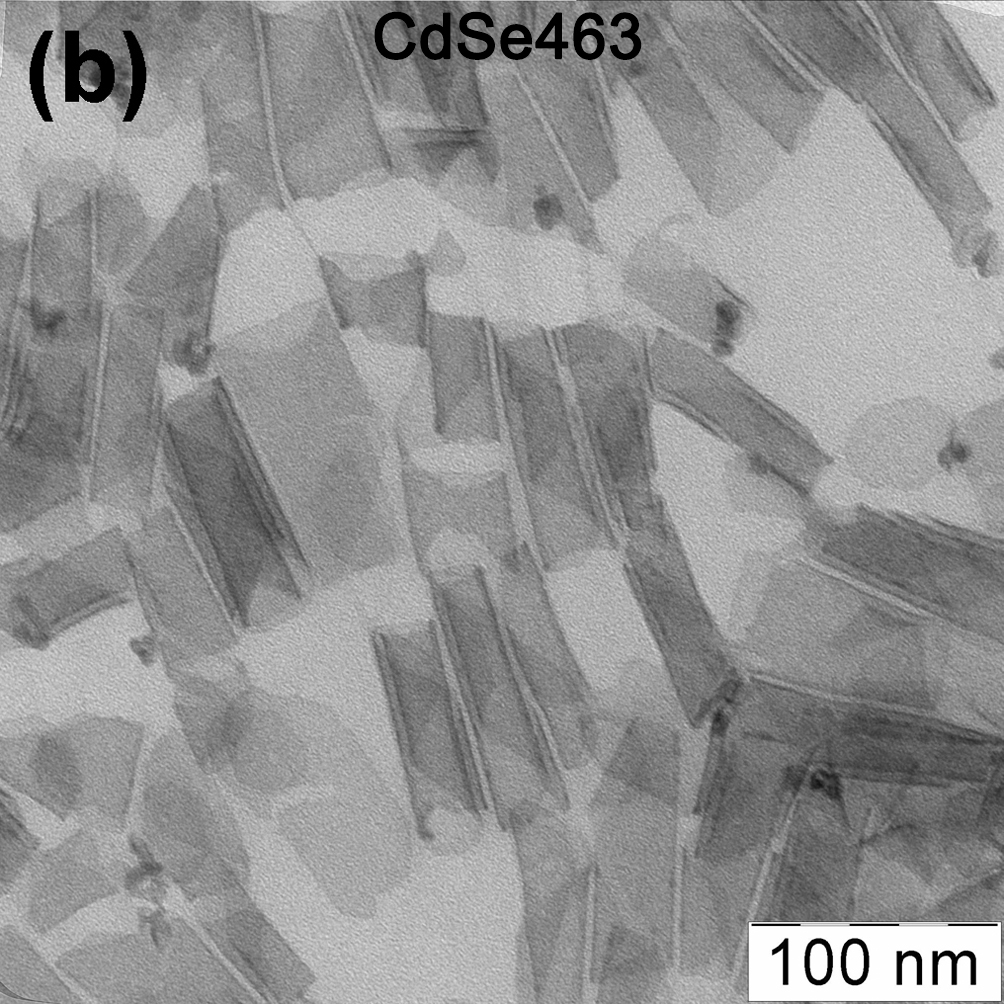
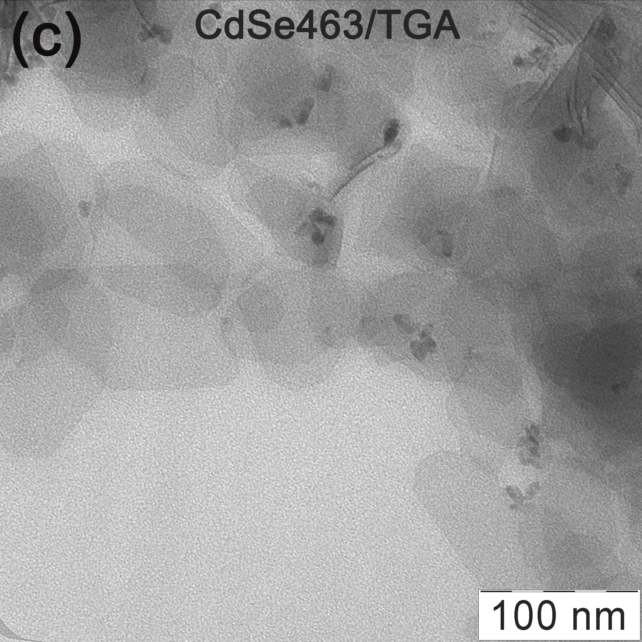

TEM studies of obtained NPLs showed that their lateral size was 100–200 nm except for CdSe512 and CdSe550 populations whose size was about 10 nm [Fig. 1(a–d)]. CdSe NPLs with large lateral size were observed to roll-up into nanoscrolls, however, after TGA treatment they unfolded to flat nanoplatelets, in agreement with the literature data. Bouet et al. (2013) According to X-ray and electron diffraction measurements, all the NPLs had the zinc-blende crystal structure.
III.2 Optical absorption and photoluminescence studies
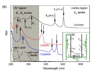
Typical absorption spectra of CdTe, CdSe, and CdS NPLs are shown in Fig. 1(e). Two well-defined narrow absorption bands for each sample appear in the visible region. These bands correspond to the transitions from the light-hole and heavy-hole valence sub-bands to the conduction band and are denoted as – and –, respectively. The spectral positions of these bands are consistent with the literature data. Ithurria and Dubertret (2008); Ithurria et al. (2011a); Pedetti et al. (2013); Li et al. (2012) In the UV region (200–400 nm), however, unexpectedly non-monotonic spectra with pronounced and intensive absorption bands was revealed, in contrast with the featureless absorption spectra typical of spherical QDs. The observed fine structure was different for various NPLs. For CdTe NPLs, three absorption bands with the width of 50–70 nm can be distinguished. These bands are wider than the – and – bands, whose widths are 6–8 and 15–20 nm, respectively. It should be noted that the shape of the UV bands is close to the Lorentz profile, which indicates the absence of inhomogeneous broadening. The UV absorption spectra of CdSe and CdS NPLs reveal a similar behavior. A single maximum was observed for CdSe463 and CdSe396 NPL populations, whereas two maxima were registered for CdS NPLs.
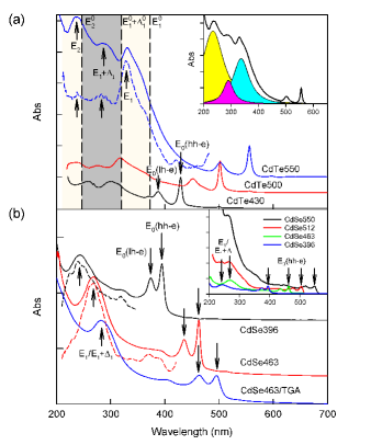
The absorption spectra of CdTe NPLs with different thickness are shown in Fig. 2(a). For all populations, three bands in UV region are observed. These bands shift to longer wavelengths with increasing thickness.
The presence of the absorption bands is supported by photoluminescence (PL) excitation spectroscopy. The PL excitation spectrum for CdTe550 NPL shown by dashed line in Fig. 2(a) clearly demonstrates the features coinciding well with those in the absorption spectrum. The PL excitation spectra and the thickness-dependent absorption spectra exclude a possible interpretation of the UV absorption bands as resulting from the traces of free oleic acid and cadmium oleate [Fig. 1(e)].
In the case of CdSe NPLs, a pronounced size effect is observed for CdSe396 and CdSe463 populations [Fig. 2(b)]. A single UV band shifts to higher energies with decreasing thickness. The PL excitation spectra also show a pronounced peak in the UV region which coincides with the absorption bands in both the samples. Additional bands at 370 and 392 nm (CdSe463) and at 319 nm (CdSe396) observed in PL excitation spectra can be attributed to the series transitions analogous to those observed in epitaxial quantum wells Winkler (1995) or an exciton formed by an electron and a hole from spin-orbit split band. Yang et al. (2013) However, this behavior does not apply to CdSe512 and CdSe550 populations whose high-energy peaks lie at higher energies as compared to their expected positions [Fig. 2(b)]. This could be a result of significantly smaller lateral size of these NPLs which is comparable to the Bohr radius of exciton in CdSe (7 nm) and so the expected 2D behavior is violated. To get additional information on the origin of the UV bands, we performed ligand exchange with thioglycolic acid to synthesize a CdSe463TGA sample covered with ligands other than the oleic acid. In this sample, the single UV band is retained but is shifted to longer wavelength [Fig. 2(b)] because of an increase in the NPL thickness resulted from the sulfide layer formation.
III.3 First-principles calculations of the band structure and absorption spectra
To calculate the band structure of NPLs, periodic structures consisting of slabs of (001)-oriented NPLs with the zinc-blende structure separated by vacuum layers were used. The nanoplatelets had a thickness n from one to six monolayers (ML) and were terminated by Cd atoms on both sides. The vacuum layer of 20 Å between the slabs was found to be sufficient to neglect the interaction between the NPL and its images. To make the nanoplatelets insulating, two terminating F atoms were added near the Cd atoms on both surfaces of the NPL to compensate the charge of electrons produced by an extra Cd plane. The energies of the on-top, hollow, and four different bridge configurations of F atoms on the surfaces of NPLs were compared; the bridge position with F atoms located near the expected Se sites of the zinc-blende structure was found to be the ground-state structure with the space group.
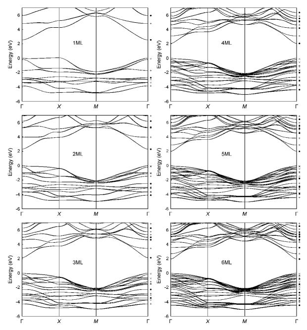
At first, the geometry of NPLs (the in-plane lattice parameter and atomic positions) was carefully optimized until the residual forces acting on the atoms decreased to below Ha/Bohr. The in-plane lattice parameter of NPLs was found to increase from 3.9513 Å for 1ML to 4.1731 Å for 6ML toward the calculated interatomic Cd–Cd distance of 4.2544 Å for bulk CdSe. The band structure of all NPLs was then calculated (Fig. 3). The scissors correction of 1.495 eV estimated from the band structure calculations for bulk zinc-blende CdSe was applied to the energies of all conduction bands of NPLs (the applicability of the scissors correction to CdSe was recently approved by calculations Zakharov et al. (1994)).
An analysis of the band structures shows that the valence band of Cdn+1SenF2 NPLs is composed of bands with the , , and symmetry at the point originating mainly from F and Se atomic states. Note a large spin-orbit splitting for bands originating from Se states (upper part of the valence band) and negligibly small splitting for bands originating from F states (lower part of the valence band).
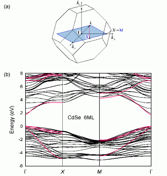
The structure of the conduction band of NPLs appeared to be different from that expected in simple theories that predict size-effect-induced shifts of dispersion curves for sub-bands. In our case, we see a number of the lower-lying bands with the and symmetry at the point originating mainly from, respectively, and empty atomic orbitals of Cd and Se. The higher-lying conduction bands have predominantly the symmetry and originate from Cd and Se states. An inspection of Fig. 3 and a comparison between the band structures of 6ML NPLs and bulk CdSe [Fig. 4(b)] shows that the number of bands below the bands can be as large as 10–14. It looks like one of three orbitals of Se, , is strongly split off and form these extra bands while the other and orbitals form the higher-lying bands with wave functions of the symmetry. As a result of a complex interaction between and atomic orbitals, a number of subbands have properties that are very different from those expected in simple theories. For example, these bands have very different effective masses (which is unusual for sub-bands). The comparison of the remaining parts of the band structures shows that there is a qualitative agreement between them: we can see the formation of dense “nodes” in the valence band along the dispersion curves of bulk CdSe when the number of monolayers is increased [see Fig. 3 and Fig. 4(b)].
IV Discussion
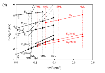
The – and – bands in the visible region can be attributed to the exciton series at the point of the BZ [Fig. 1(c), inset] and are related to the fundamental absorption edge. In the UV region, the behavior of the absorption bands is different. Although for different chalcogenides different fine structure of these bands was observed, in all cases the absorption fine structure in NPLs looks very similar to that in bulk crystals. Ninomiya and Adachi (1995a); Adachi et al. (1993); Kim et al. (1994); Ninomiya and Adachi (1995b) Three bands observed for CdTe NPLs in the UV region may be associated with , , and transitions found in bulk CdTe. Ninomiya and Adachi (1995a) The single UV band observed for CdSe NPLs can be explained by an overlapped and transitions resulting from weaker spin-orbital coupling. This agrees with the optical spectra for bulk zinc-blende CdSe in the UV region, in which a pronounced peak and a shoulder for transition were observed. Adachi et al. (1993); Kim et al. (1994) Two UV bands observed for CdS NPLs are in agreement with two maxima observed for CdSe Kim et al. (1994) (however, it should be noted that the data in Ref. Ninomiya and Adachi, 1995b are obtained for wurtzite CdS). In all cadmium chalcogenide NPLs, the UV bands are shifted towards shorter wavelengths as compared to the data for bulk compounds. In Fig. 2(c), we plotted their energies as a function of the reciprocal square of the thickness . The NPL thickness values were taken from the literature. Ithurria et al. (2011a); Pedetti et al. (2013) The linear dependence of on for all exciton series confirms the size effect. The asymptotic energies in the limit are close to the energies of the corresponding transitions in bulk compounds. Ninomiya and Adachi (1995a); Adachi et al. (1993) For UV bands, the thickness dependence of the shifts is weaker than that for the series; this may indicate a larger effective mass of charge carriers.
The hypothesis about the relation between the UV absorption bands and optical and transitions at the boundary of the BZ needs a detailed analysis. For bulk cadmium chalcogenides with zinc-blende structure, these high-energy transitions are known to occur at the point ( and transitions) and the point ( transition) of the 3D BZ. In the case of quasi-2D nanoplatelets, the 3D BZ transforms to its 2D projection [Fig. 4(a)]: the point becomes the point at corner of square, and the point (which does not exist in 2D BZ) is projected to the point at the middle of its side. The comparison of the band structures for a typical F-terminated CdSe NPL with a thickness of 6 ML and bulk CdSe [Fig. 4(b)] shows a good agreement between the dispersion curves at the band edges. This means that the energies of the band extrema at the boundary of the 2D BZ are close to those in the band structure of bulk CdSe. This fact supports our interpretation of the UV absorption bands as resulting from the optical transitions at the and points of the 2D BZ.
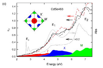
In order to give further evidences for our interpretation, we performed first-principles modeling of the absorption spectrum for CdSe463 NPL. The calculated absorption spectra for the in-plane and out-of-plane light polarizations (red and black dashed lines), the absorption spectrum averaged over polarizations (solid black line), and partial contributions into this spectrum from different points of 2D Brillouin zone (color shaded areas; the BZ regions used for integration are shown by shaded areas on the inset) are compared with the experimental spectrum (grey line) and the calculated absorption spectrum for bulk CdSe (dotted line) in Fig. 4(c). It is evident that the main contributions to the and bands originate from and points of the BZ, respectively, not from the point. This explains weaker thickness-dependent shifts observed for these transitions. The agreement between the modeled and experimental spectra in the region is good. The position of the band lies outside of our experimentally available wavelength range. The excitonic features in the low-energy part of the spectrum are not reproduced because our calculations did not take into account the excitonic effects. It should be noted that the appearance of distinct and exciton peaks in the absorption spectra of NPLs is due to the specific features of their electronic structure that results in step-like or divergent van Hove singularities. Winkler (1995)
| Parameter | CdTe | CdSe |
|---|---|---|
| Band gap (eV) | 1.49 | 1.66 |
| Kane energy (eV) | 21 | 16.5 |
| Spin-orbit splitting (eV) | 0.6 | 0.39 |
| 0.13 | 1.54 | |
| 0.99 | 0.18 | |
| 0.52 | 0.65 | |
| () | 0.11 | 0.183 |
| () | 0.69 | 0.89 |
| Dielectric constant | 10.4 | 9.6 |
| Lattice constant (nm) | 0.648 | 0.608 |
The contribution of the exciton transitions at the point was analyzed within the eight-band Pidgeon–Brown model. In this model, the bulk band dispersion is characterized in terms of the band parameters, which include the bulk band gap energy , the Kane energy , the valence band spin-orbit splitting , the remote band contribution to the electron effective mass , and the valence band Luttinger–Kohn parameters and . The parameters used for CdTe and CdSe NPLs were taken from Refs. Ithurria et al., 2011a; Adachi, 2009 and are summarized in Table 1. The effective-mass approximation was applied with an assumption of an infinite potential-barrier height and the energies of low-energy – and – transitions were calculated. We assumed that the in-plane wave vector and the out-of-plane wave vector component , where is the confinement quantum number and is the thickness of the NPL. The thickness dependence of exciton transition energies was found for . The calculated energies for CdTe NPLs are shown in Fig. 2(c) by dashed lines. Lowest-energy transitions are in good agreement with the experimental data. A similar behavior was observed for CdSe NPLs. However, the thickness dependence of the higher-order transitions deviates from the experimentally observed one, which possibly indicates that higher-order transitions are weaker than the transitions at the boundary of BZ.
V Conclusions
In summary, we have revealed that cadmium chalcogenide NPLs exhibit distinct and intensive exciton bands with a pronounced size effect not only in the visible region, but also in the UV region. We have shown that these high-energy bands are associated with the , , and exciton transitions occurring at the and points of the 2D BZ of NPL, which originates from and points of the BZ of bulk crystals. This behavior is general for all 2D NPLs and contrasts with the behavior of spherical QDs made of cadmium chalcogenides. Thickness-dependent shift of the absorption bands in the NPLs reveals tunable optical properties of them not only in the visible, but in the UV spectral region too. The specific features of the UV absorption spectra resulting from step-like or divergent van Hove singularities typical of quasi-2D NPLs may attract a fundamental interest to an analysis of the electronic transitions in other 2D semiconductor systems deep into the Brillouin zone. The UV features of the NPL absorption spectra may be interesting from a practical perspective for the development of UV photodetectors and other optoelectronic devices.
Acknowledgements.
This work was supported by the Russian Foundation for Basic Research (grants No. 16-03-00704, 16-29-11694, 15-02-05856, and 16-29-11805).References
- Talapin et al. (2010) D. V. Talapin, J.-S. Lee, M. V. Kovalenko, and E. V. Shevchenko, Chem. Rev. 110, 389 (2010).
- Lan et al. (2014) X. Lan, S. Masala, and E. H. Sargent, Nat. Mater. 13, 233 (2014).
- Hetsch et al. (2013) F. Hetsch, N. Zhao, S. V. Kershaw, and A. L. Rogach, Materials Today 16, 312 (2013).
- Shirasaki et al. (2013) Y. Shirasaki, G. J. Supran, M. G. Bawendi, and V. Bulović, Nat. Photon. 7, 13 (2013).
- Vasiliev et al. (2011) R. B. Vasiliev, D. N. Dirin, and A. M. Gaskov, Russ. Chem. Rev. 80, 1139 (2011).
- Peng et al. (2000) X. Peng, L. Manna, W. Yang, J. Wickham, E. Scher, A. Kadavanich, and A. P. Alivisatos, Nature 404, 59 (2000).
- Kuno et al. (2006) M. Kuno, O. Ahmad, V. Protasenko, D. Bacinello, and T. H. Kosel, Chem. Mater. 18, 5722 (2006).
- Deka et al. (2010) S. Deka, K. Miszta, D. Dorfs, A. Genovese, G. Bertoni, and L. Manna, Nano Lett. 10, 3770 (2010).
- Manna et al. (2003) L. Manna, D. J. Milliron, A. Meisel, E. C. Scher, and A. P. Alivisatos, Nat. Mater. 2, 382 (2003).
- Kanaras et al. (2005) A. G. Kanaras, C. Sōnnichsen, H. Liu, and A. P. Alivisatos, Nano Lett. 5, 2164 (2005).
- Ithurria and Dubertret (2008) S. Ithurria and B. Dubertret, J. Am. Chem. Soc. 130, 16504 (2008).
- Ithurria et al. (2011a) S. Ithurria, M. D. Tessier, B. Mahler, R. P. S. M. Lobo, B. Dubertret, and A. L. Efros, Nat. Mater. 10, 936 (2011a).
- Chen et al. (2014) Z. Chen, B. Nadal, B. Mahler, H. Aubin, and B. Dubertret, Adv. Funct. Mater. 24, 295 (2014).
- Fan et al. (2015) F. Fan, P. Kanjanaboos, M. Saravanapavanantham, E. Beauregard, G. Ingram, E. Yassitepe, M. M. Adachi, O. Voznyy, A. K. Johnston, G. Walters, G.-H. Kim, Z.-H. Lu, and E. H. Sargent, Nano Lett. 15, 4611 (2015).
- Vitukhnovsky et al. (2015) A. G. Vitukhnovsky, V. S. Lebedev, A. S. Selyukov, A. A. Vashchenko, R. B. Vasiliev, and M. S. Sokolikova, Chem. Phys. Lett. 619, 185 (2015).
- Grim et al. (2014) J. Q. Grim, S. Christodoulou, F. Di Stasio, R. Krahne, R. Cingolani, L. Manna, and I. Moreels, Nat. Nanotech. 9, 891 (2014).
- She et al. (2014) C. She, I. Fedin, D. S. Dolzhnikov, A. Demortière, R. D. Schaller, M. Pelton, and D. V. Talapin, Nano Lett. 14, 2772 (2014).
- Lhuillier et al. (2015) E. Lhuillier, J.-F. Dayen, D. O. Thomas, A. Robin, B. Doudin, and B. Dubertret, Nano Lett. 15, 1736 (2015).
- Sigle et al. (2015) D. O. Sigle, L. Zhang, S. Ithurria, B. Dubertret, and J. J. Baumberg, J. Phys. Chem. Lett. 6, 1099 (2015).
- Achtstein et al. (2014) A. W. Achtstein, A. V. Prudnikau, M. V. Ermolenko, L. I. Gurinovich, S. V. Gaponenko, U. Woggon, A. V. Baranov, M. Y. Leonov, I. D. Rukhlenko, A. V. Fedorov, and M. V. Artemyev, ACS Nano 8, 7678 (2014).
- Feldmann et al. (1987) J. Feldmann, G. Peter, E. O. Göbel, P. Dawson, K. Moore, C. Foxon, and R. J. Elliott, Phys. Rev. Lett. 59, 2337 (1987).
- Tessier et al. (2012) M. D. Tessier, C. Javaux, I. Maksimovic, V. Loriette, and B. Dubertret, ACS Nano 6, 6751 (2012).
- Tessier et al. (2013) M. D. Tessier, B. Mahler, B. Nadal, H. Heuclin, S. Pedetti, and B. Dubertret, Nano Lett. 13, 3321 (2013).
- Achtstein et al. (2015) A. W. Achtstein, A. Antanovich, A. Prudnikau, R. Scott, U. Woggon, and M. Artemyev, J. Phys. Chem. C 119, 20156 (2015).
- Klimov (2000) V. I. Klimov, J. Phys. Chem. B 104, 6112 (2000).
- de Mello Donegá and Koole (2009) C. de Mello Donegá and R. Koole, J. Phys. Chem. C 113, 6511 (2009).
- Dirin et al. (2011) D. N. Dirin, M. S. Sokolikova, A. M. Gaskov, and R. B. Vasilev, J. Opt. Technol. 78, 693 (2011).
- Angeloni et al. (2016) I. Angeloni, W. Raja, R. Brescia, A. Polovitsyn, F. De Donato, M. Canepa, G. Bertoni, R. Proietti Zaccaria, and I. Moreels, ACS Photonics 3, 58 (2016).
- Pedetti et al. (2013) S. Pedetti, B. Nadal, E. Lhuillier, B. Mahler, C. Bouet, B. Abécassis, X. Xu, and B. Dubertret, Chem. Mater. 25, 2455 (2013).
- Ithurria et al. (2011b) S. Ithurria, G. Bousquet, and B. Dubertret, J. Am. Chem. Soc. 133, 3070 (2011b).
- Li et al. (2012) Z. Li, H. Qin, D. Guzun, M. Benamara, G. Salamo, and X. Peng, Nano Res. 5, 337 (2012).
- Ithurria and Talapin (2012) S. Ithurria and D. V. Talapin, J. Am. Chem. Soc. 134, 18585 (2012).
- Garrity et al. (2014) K. F. Garrity, J. W. Bennett, K. M. Rabe, and D. Vanderbilt, Comput. Mater. Sci. 81, 446 (2014).
- Bouet et al. (2013) C. Bouet, B. Mahler, B. Nadal, B. Abecassis, M. D. Tessier, S. Ithurria, X. Xu, and B. Dubertret, Chem. Mater. 25, 639 (2013).
- Winkler (1995) R. Winkler, Phys. Rev. B 51, 14395 (1995).
- Yang et al. (2013) J. Yang, J. S. Son, J. H. Yu, J. Joo, and T. Hyeon, Chem. Mater. 25, 1190 (2013).
- Zakharov et al. (1994) O. Zakharov, A. Rubio, X. Blase, M. L. Cohen, and S. G. Louie, Phys. Rev. B 50, 10780 (1994).
- Ninomiya and Adachi (1995a) S. Ninomiya and S. Adachi, J. Appl. Phys. 78, 4681 (1995a).
- Adachi et al. (1993) S. Adachi, T. Kimura, and N. Suzuki, J. Appl. Phys. 74, 3435 (1993).
- Kim et al. (1994) Y. D. Kim, M. V. Klein, S. F. Ren, Y. C. Chang, H. Luo, N. Samarth, and J. K. Furdyna, Phys. Rev. B 49, 7262 (1994).
- Ninomiya and Adachi (1995b) S. Ninomiya and S. Adachi, J. Appl. Phys. 78, 1183 (1995b).
- Adachi (2009) S. Adachi, Properties of Semiconductor Alloys: Group-IV, III-V and II-VI Semiconductors (John Wiley & Sons Ltd., 2009).