First-principles study of spin texture and Fermi lines in Bi(111) multi-layer nanofilm
Abstract
We have performed a fully relativistic first-principles density functional calculation examining the surface state of bismuth (Bi) (111) multi-layer nanofilm, with up to 20 Bi bilayers, and investigated the Rashba effect and spin texture on the Bi surfaces. We have revealed a giant out-of-plane spin states on the Fermi lines, and the maximum value of the out-of-plane spin component being approximately 40 of the magnitude of the total spin. We have also evaluated the Rashba parameter Å using the surface state bands which is buried in the bulk state, at -0.32 eV below the Fermi energy.
pacs:
I Introduction
Understanding the transport properties of bismuth(Bi) has long been a major aim in the field of condensed matter physics. The anomalous transport properties occur in this material, originating from its semimetallic electronic structuresIssi (1979), in which electron and hole carriers coexist. In addition, the Bi atom has a strong spin-orbit interaction(SOI) originating from its high atomic number(83). Therefore, it is expected that various relativistic effects apply, such as the Rashba effectRashba (1960), the quantum spin Hall effectMurakami (2006), and conversion between the spin and charge currentsRojas Sánchez et al. (2013).
Bi films are expected to be suitable for device applicationNagao et al. (2004) as it has been shown that flat thin films can be grown on a Si (111) surface. In this case, the surface state differs strongly from the bulk state; that is the surface density of states is significantly larger than that of the bulk statesHirahara et al. (2006). As a result of the strong SOI within the electronic structures, spintronic applications are expected.
Recent angle-resolved photo-emission spectroscopy (ARPES) experiments Takayama et al. (2011) have revealed the novel spin textures of the surface states of Bi thin films. The conventional Rashba (in-plane) spin texture and a giant out-of-spin component are detected. The spin texture has been analyzed using the tight-binding modelSaito et al. (2016); quantitative analysis of the spin textures based on the first-principles calculations has not been conducted.
In this paper, we conduct a theoretical quantitative investigation of the surface states of Bi (111) multi-layer nanofilm based on the Fermi lines.
Using fully relativistic first-principles density functional calculations,
we perform quantitative analysis for the surface localized spin vortexes on the Fermi lines of the Bi thin film.
Our calculation supports the experimentally observed large out-of-plane spin component.
Further, we find that the Rashba parameter of these bands is large (approximately 1.9 0.1 eV).
II theoretical method
Using the OpenMX codeOpe , we perform fully relativistic first-principles calculations based on density functional theory (DFT) within the generalized gradient approximation (GGA)Perdew et al. (1996). In our study, wavefunctions are expressed as a linear combination of multiple pseudo atomic orbitals (LCPAO) generated by a confinement schemeOzaki and Kino (2005); Ozaki (2003); Ozaki and Kino (2004).
We deduce the spin polarization in the reciprocal lattice vector k from the spin density matrix. The spin density matrices are calculated using the spinor Bloch wavefunction, the component of which is given by , which is obtained from the OpenMX calculations, where is the spin index ( or ) and is the band index. Thus,
| (1) | |||||
| (2) |
where is the overlap integral of the -th and -th localized orbitals and is expansion coefficient.
is the -th lattice vector.
We evaluated spin vector component (, , ) from density matrices.
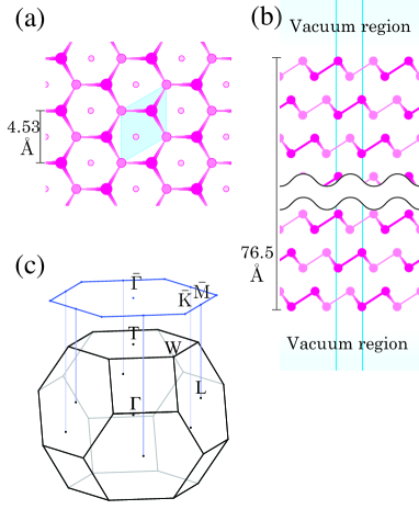
We perform first-principles calculations of 20-bilayer Bi (111) film (Fig. 1). The length of the in-plane unit vector is 4.53 Å, and the thickness of the film is 76.5 Å. Further, each bilayer forms a honeycomb lattice and has 1.6 Å-buckling.
We confirm that the Fermi lines are insensitive to the thickness when more than 13 bilayer films are used.
In the 20-bilayer slab calculation, the interaction between the two surfaces is expected to be very weak and can be neglected. As the slab has inversion symmetry, the Kramers degenerate bands appear. Because of the weak interaction between two surfaces, unitary transformation of the two bands generates to wavefunctions that are localized at each surface. By analyzing the wavefunctions, we can obtain information on the surface states.
III Band structure and surface states
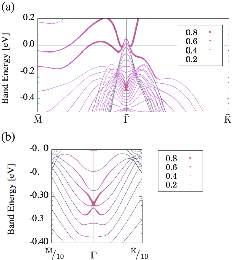
Figure 2(a) shows the band structure of the 20-bilayer Bi (111) thin film. The surface localization ratio is represented by the circle radius proportional to the number of electrons within the surface-1bilayer. Near the Fermi level along the - line, two surface-localized bands appear. The surface bands are connected to the bulk-like bands around the point near the , at which states the bands have small amplitude on the surface layer. The bulk-like bands originate from the hole pocket at the point in the bulk structure Bi
On the other hand, as shown in fig. 2(b), the surface localized states at the point are buried in the bulk-like state in the region of - = -0.32 eV, where is band energy. More than 50% of these states are localized in the surface 1-bilayer. These bands cross at the point, and the energy contours form circular shape. In addition, the spin texture indicated by these bands corresponds to a typical in-plane spin vortex. These features appear to conform to a typical Rashba band. We estimate the Rashba parameter from the gradient of these bands. The estimated is 1.9 0.1 eVÅ, which is very large and is of the same order as the value obtained for other bismuth compounds (e.g., BiTeI has = 3.8eVÅ Ishizaka et al. (2011)).
IV Fermi lines and surface localization
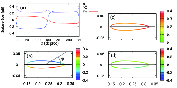
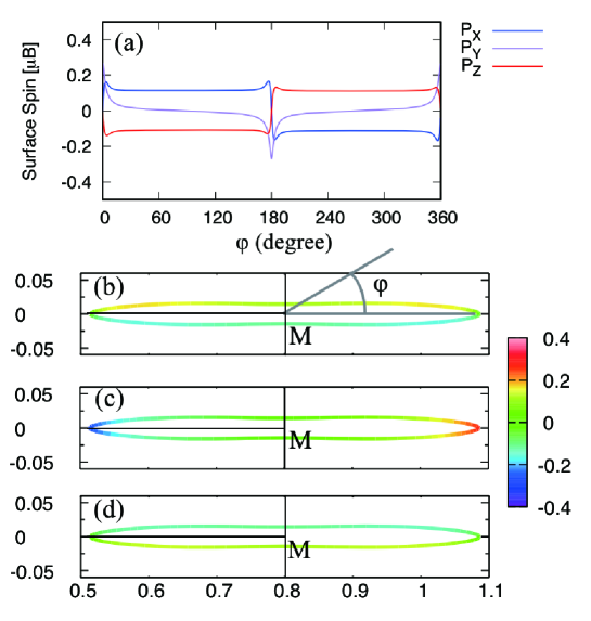
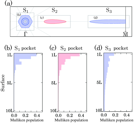
Figure 3(a) shows the Fermi lines of a freestanding 20-bilayer Bi (111) film. There are two electron pockets (S1 and S3) and one hole pocket (S2). S1, S2, and S3 have hexagonal, elliptical, and needle-like shapes, respectively. These features are consistent with those observed in previous studies based on ARPES experimentHirahara et al. (2006); Takayama et al. (2011).
To perform quantitative analysis of the Fermi lines, we estimate the area of each pocket and compare the results with the ARPES-derived experimental valuesTakayama et al. (2012). The calculated areas of the S1, S2 and S3 pockets are 8.7 10-3[Å-2], 4.4 10-3[Å-2] and 7.7 10-3[Å-2], respectively. The area of each pocket are close to those observed in the ARPES experimentsTakayama et al. (2012).
Next, in order to investigate the surface localization states, we calculate the Mulliken population from the LCPAO parameter. In the S1 and S2 pockets, more than 60% of the wave functions components are in the surface 1-bilayer and more than 90% of the components are in the surface 2-bilayer (Fig. 3(b)- (c)). The electron density derived from the S3 pocket is more delocalized than those for the S1 and S2 pockets, and only 30% of the wavefunction components are in the surface 1-bilayer(Fig. 3(d)). The surface localization of each pocket corresponds to the intensities obtained from the ARPES experiments; therefore S1 and S2 pockets are expected to have strong intensity, while the S3 pockets are expected to have weak intensity. This is consistent with the ARPES experimentsTakayama et al. (2012). The difference in localization for each of the Fermi lines originates from the direct band gap of bulk Bi. The direct energy gaps in the bulk Bi are 0.26 eV and 0.11eV at the and points (Fig.1 (c)), respectively, where the and the points of the bulk Bi correspond to the and points of the Bi film, respectively. The small direct energy gap may cause the surface delocalization at the point.
V Surface-projected spin texture in momentum space
Next, we discuss whether the spin textures on the Fermi lines are typical in-plane Rashba-type spin or non-Rashba-type spin vortices including a giant out-of-plane spin component.
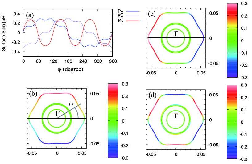
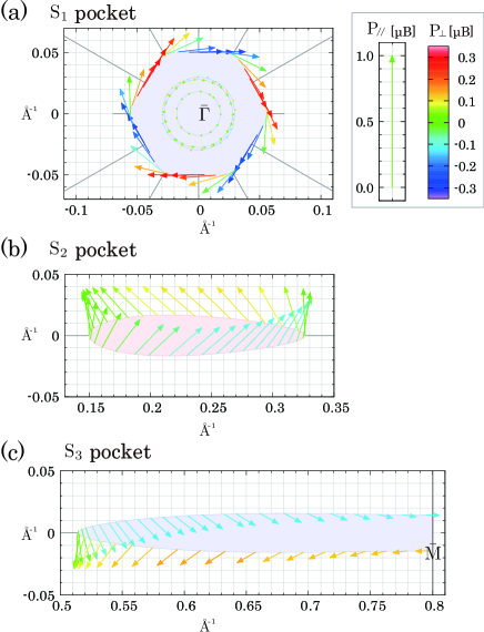
Figures 4(a) - (c) show the Fermi lines and surface-localized spin texture (in-plane spin component P, out-of-plane spin component ) projected onto surface 1-bilayer.
The vector length shows the magnitude of , whereas that of is expressed by the color bar.
In S1 pocket, has clockwise vortex and has rotational periodicity.
The magnitude of has the maximum value at line and minimum value 0 at the line.
The maximum magnitude of the is 40% of the spin vector.
These features are in reasonably good agreement with the result of ARPES experimentTakayama et al. (2011)
and can be explained via group theoretical analysis.
The obtained spin textures in momentum space depend on the symmetry group. The first-order spin Hamiltonian over the wave vector is expressed as , where is the -th component of the wave vector and is the Pauli-matrix. () runs over and (, , and ). The spin Hamiltonian satisfies the following expression via effective symmetric operation :. The point has symmetry. (if we consider the two surfaces, the symmetry is .) The in-plane spin texture in the Bi surface can be explained by the first-order term of the spin Hamiltonian, Oguchi and Shishidou (2009). On the other hand, the out-of-plane spin component is not explained by the first-order term, but is instead explained by the third-order term of Hamiltonian, expressed as Vajna et al. (2012). The out-of-plane spin components on the line are zero, because it is on the - plane(=0). In the Bi surface, third-order is very important, and this feature is similar to the result of a our previous study on the Bi 1-bilayerKotaka et al. (2012).
The first-order term of the spin Hamiltonian on the line is expressed as . Therefore, the S2 and S3 pockets are consistent with this spin Hamiltonian. The origin of out-of-plane spin component is different from S1 pocket.
More detail information of spin textures is provided in supplementarysuppl .
VI Summary
We performed fully-relativistic first-principles density functional calculations of the surface state of the Bi (111) multi-layer nanofilm.
We investigated the surface-localized spin texture of the 20-bilayer Bi nanofilm,
and we focused on the giant out-of-plane spin.The maximum magnitude of the P is 40% of the spin vector.
In addition, we revealed the surface-localized typical Rashba spin-split state,
which is buried in the bulk states.
The Rashba parameter Å was
evaluated using these surface state bands.
When this work was almost completed,
a recent paper Saito et al. (2016) regarding the tight-binding calculation of spin split states in Bi thin film come to our attention.
The out-of-plane spin and the differences in the localization of the Fermi lines reported in that study are qualitatively consistent with our first-principles results.
VII acknowledgments
The author would like to thank T. Oguchi, A. Takayama, T. Okuda and T. Aono for invaluable discussions.
Part of this research has been funded by the MEXT HPCI Strategic Program. This work was partly supported by Grants-in-Aid for Scientific Research (Nos. 25390008, 25790007, 26108708 and 15H01015) from the JSPS and by the RISS project in the IT program of MEXT. One of the authors (H.K.) thanks JSPS for the financial support (No. 22-2329). The computations in this research were performed using the supercomputers at the ISSP, University of Tokyo, the RCCS, Okazaki National Institute, and the IMR, Tohoku University.
References
- Issi (1979) J.-P. Issi, Australian Institute of Physics 32, 585 (1979).
- Rashba (1960) I. E. Rashba, Sov. Phys. Solid. State. 2, 1109 (1960).
- Murakami (2006) S. Murakami, Phys. Rev. Lett 97, 236805 (2006).
- Rojas Sánchez et al. (2013) J. C. Rojas Sánchez, L. Vila, G. Desfonds, S. Gambarelli, J. P. Attane, J. M. De Teresa, C. Magen, and A. Fert, Nat. Commun. 4 (2013).
- Nagao et al. (2004) T. Nagao, J. T. Sadowski, M. Saito, S. Yaginuma, Y. Fujikawa, T. Kogure, T. Ohno, Y. Hasegawa, S. Hasegawa, and T. Sakurai, Phys. Rev. Lett 93, 105501 (2004).
- Hirahara et al. (2006) T. Hirahara, T. Nagao, I. Matsuda, G. Bihlmayer, E. V. Chulkov, Y. M. Koroteev, P. M. Echenique, M. Saito, and S. Hasegawa, Phys. Rev. Lett. 97, 146803 (2006).
- Takayama et al. (2011) A. Takayama, T. Sato, S. Souma, and T. Takahashi, Phys. Rev. Lett. 106, 166401 (2011).
- Saito et al. (2016) K. Saito, H. Sawahata, T. Komine, and T. Aono, Phys. Rev. B 93, 041301 (2016).
- (9) OpenMX web site, http://www.openmx-square.org/.
- Perdew et al. (1996) J. P. Perdew, K. Burke, and M. Ernzerhof, Phys. Rev. Lett. 77, 3865 (1996).
- Ozaki and Kino (2005) T. Ozaki and H. Kino, Phys. Rev. B 72, 045121 (2005).
- Ozaki (2003) T. Ozaki, Phys. Rev. B 67, 155108 (2003).
- Ozaki and Kino (2004) T. Ozaki and H. Kino, Phys. Rev. B 69, 195113 (2004).
- Ishizaka et al. (2011) K. Ishizaka, M. S. Bahramy, H. Murakawa, M. Sakano, T. Shimojima, T. Sonobe, K. Koizumi, S. Shin, H. Miyahara, A. Kimura, et al., Nat. Mater. 10, 521 (2011).
- Takayama et al. (2012) A. Takayama, T. Sato, S. Souma, T. Oguchi, and T. Takahashi, Nano Lett. 12, 1776 (2012).
- Oguchi and Shishidou (2009) T. Oguchi and T. Shishidou, J. Phys. Condens. Matter 21, 092001 (2009).
- Vajna et al. (2012) S. Vajna, E. Simon, A. Szilva, K. Palotas, B. Ujfalussy, and L. Szunyogh, Phys. Rev. B 85, 075404 (2012).
- Kotaka et al. (2012) H. Kotaka, F. Ishii, M. Saito, T. Nagao, and S. Yaginuma, Jpn. J. Appl. Phys. 51, 025201 (2012).
- (19) See Supplemental Material at [URL] for details of the spin textures on the each pockets S1, S2, S3.
Supplemental Materials