Antireflective photonic structure for coherent nonlinear spectroscopy
of single magnetic quantum dots
Abstract
This work presents epitaxial growth and optical spectroscopy of CdTe quantum dots (QDs) in (Cd,Zn,Mg)Te barriers placed on the top of (Cd,Zn,Mg)Te distributed Bragg reflector. The formed photonic mode in our half-cavity structure permits to enhance the local excitation intensity and extraction efficiency of the QD photoluminescence, while suppressing the reflectance within the spectral range covering the QD transitions. This allows to perform coherent, nonlinear, resonant spectroscopy of individual QDs. The coherence dynamics of a charged exciton is measured via four-wave mixing, with the estimated dephasing time ps. The same structure contains QDs doped with single Mn2+ ions, as detected in photoluminescence spectra. Our work therefore paves the way toward investigating and controlling an exciton coherence coupled, via ,- exchange interaction, with an individual spin of a magnetic dopant.
I Introduction
Distributed Bragg Reflectors (DBRs) are typically applied to enhanceWang (1974); Sadowski et al. (1997); Benisty et al. (1998); Ng et al. (1999); Tawara et al. (2000); Guo et al. (2000); Pacuski et al. (2009); Gust et al. (2009); Rousset et al. (2013); Koba and Suffczyński (2013, 2014); Jakubczyk et al. (2014) the reflectance (), but the opposite result — a very low — can be also designed and obtained with the use of DBRs Schubert et al. (2008); Chhajed et al. (2008). Such antireflection (AR) stacks are particularly useful in resonant optical spectroscopy, where the reflected laser light dominates the investigated signal substantially. In particular, using four-wave mixing (FWM) for probing the coherence of single quantum dots (QDs), necessitates efficient injection of the optical excitation into the hetero-structure, so as to reach the field amplitude at the QD location sufficient to induce its FWM. This condition has been achieved by employing AR planar samples Langbein and Patton (2006); Patton et al. (2006); Kasprzak et al. (2013) and, more recently, by suitably designed nanophotonic devices Kasprzak et al. (2010); Fras et al. (2016); Mermillod et al. (2016). Here, we realize half-cavity AR planar structures and employ them to investigate FWM of individual CdTe QDs. As the same structure contains QDs with incorporated single Mn2+ ions, the appealing prospect of our work is to reveal the exciton’s coherence coupled with a magnetic dopant via ,- exchange interaction.
There are two basic approaches to AR structures on the top of high refractive index () semiconductors. Firstly, one can deposit a single layer with a lower refractive index equal to and thickness of , where is the targeted wavelength for the lowest reflectance. While this method offers a broad AR spectral range, its implementation is conditioned by the availability of materials with a required value of . Secondly, one can use symmetric microcavities composed of two DBRs with the nominally the same . The cavity mode exhibits a pronounced dip in the spectrum, which should be accurately fitted to the wavelength of interest. In this work, we implement the AR strategy based on a cavity system. In order to maximize the spectral width of the cavity resonance, we have designed and grown a low Q-factor structure (): a half-cavity is formed by four bottom Bragg pairs and the spacer containing the QD layer, also acting as a semiconductor/air interface at the top.
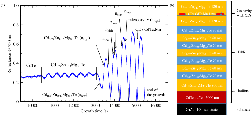
II Growth and the sample layout
The sample was grown using molecular beam epitaxy (MBE) model SVT Associates. Our molecular sources were standard Knudsen cells loaded with commercially available materials: Zn, Cd, and Te with 7 N purity; Mg and Mn with 6 N purity. Chamber pressure was at level of about Torr. The growth was assisted by in-situ optical reflectance (model Filmetrics F-30) with a white light incident beam perpendicular to the sample surface. The system is equipped with a heated optical viewport, so that it was possible to perform spectroscopic measurement during a long growth sequence, while avoiding material deposition on the window. For the sample described in this work, we monitored versus time at nm, as shown in Fig. 1 (a). In our method, this choice defined the resonant wavelength of the cavity for a given spot of the sample (the substrate was not rotated during the growth). However, other zones of the sample exhibit either thinner layers with cavity resonance at shorter wavelength or thicker layers with resonance at longer wavelength.
The growth was performed at constant temperature T = 345∘ C, on a 2-inch GaAs:Si substrate oriented (100) with 2∘ off. We started by depositing a 3m thick CdTe buffer. Since CdTe is absorbing at nm, the corresponding oscillations of were rapidly suppressed and a characteristic was measured before time s. As depicted in Fig. 1 (b), we next grew a Cd0.77Zn0.13Mg0.10Te buffer lattice matched to subsequent DBR layers. Due to the presence of Mg and Zn, such buffer exhibits a slightly lower refractive index than CdTe and meV larger energy gap than CdTe. Therefore, Cd0.77Zn0.13Mg0.10Te buffer is transparent for nm, generating interferences in the trace (time between 10400 s and 13100 s in Fig. 1 a) during the growth of this material. Observation of interferences allowed us to determine growth rate v = 1.1 m/h. Next, when reached a local maximum, we started the growth of lattice matched DBRs composed of Cd0.43Zn0.07Mg0.50Te (low layer) and Cd0.77Zn0.13Mg0.10Te (high layer) Rousset et al. (2013, 2015); Mirek et al. (2017). Adjacent layers with various composition of Mg were obtained using a pair of Mg sources, such that either one or two sources were opened at a time. An exact time-point for growing DBRs was not predefined in the programmed sequence. Instead, it was adjusted manually by closing one of the Mg shutters, as soon as the minimum of was reached, while keeping opened both Mg shutters when the maximum of was attained (see Fig. 1 (a)). As expected, during the initial stage of a DBR growth, after each pair, the contrast between the maximum and minimum value of was increasing. Interestingly, reached the minimum value below 1 already after depositing the fourth DBR pair. Since this is what required for an efficient AR structure and further DBR growth would only increase reflectance, we completed the growth of DBRs already after four pairs and we completed cavity composed of the high material Cd0.77Zn0.13Mg0.10Te, enclosing CdTe:Mn QDs in the middle. As shown in Fig. 1 (a), fabricating thickness equal to or of high index material does not affect at nm. Our half-cavity structure is formed and terminated by the semiconductor/air interface on the top.
QDs are formed out of about 1 nm (3 monolayers) thick CdTe:Mn layer grown at the same conditions as Cd0.77Zn0.13Mg0.10Te and the remaining top part of the sample. Basing on giant Zeeman effectGaj and Kossut (2011) measured for thicker CdTe:Mn layers grown in similar conditions, expected concentration of Mn in our CdTe:Mn layer is about . As a matter of fact, this layer forms a thin quantum well exhibiting interface fluctuations, leading to formation of QDs. The growth of similar QDs, but in Cd0.7Mg0.3Te barriers, was previously reported Besombes and Boukari (2014). Here, we used even lower barriers and consequently we shifted the QD emission energy to spectral region where the absorption of (Cd,Zn,Mg)Te is low enough to realize microcavities.
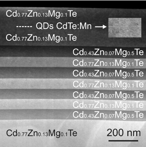
Microscopy image of the most important parts of studied structure is shown in Fig. 2. DBR layers, seen as alternating bright and dark layers, are well resolved. Also, the QD layer is resolved in the middle of the cavity, it is seen as a thin trace in the magnified part of the cavity.
III Optical spectroscopy
Photoluminescence and reflectance.
Fig. 3 shows low temperature photoluminescence (PL) and reflectance spectra of studied sample, both measured using experimental setup equipped in a microscope objective with spatial resolution of about 1m Sawicki et al. (2015). PL was excited nonresonantly at 532 nm using CW power of about 1 W, well below the QD saturation. The reflectance was measured using a white (halogen) lamp.
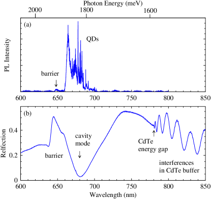
The PL reveals a signal from a thin CdTe layer at 665 nm and sharp lines of individual CdTe QDs in range 670-700 nm. In our sample, CdTe QDs are placed in Cd0.77Zn0.13Mg0.10Te barrier, which is also visible as a weak peak close to 650 nm in the PL spectrum and as a spectral wiggle in between 635 and 650 nm. We therefore estimate the confinement energy of around 50 meV for the excitons localized in QD-like states. Reflectance spectrum at the investigated area of the wafer shows also a broad (about 40 nm wide) and deep (below 3 of reflectance) cavity mode centered at 670 nm, in resonance with the emission of QDs. The obtained broad and deep cavity mode, mimics an AR coating, but also provides a local excitation intensity enhancement for the spectral and spatial location of QDs. During the growth was minimized for 730 nm (Fig. 1 (a)) for the center of the sample, but as shown in Fig 3 (b), owing to the thickness gradients, other parts of the wafer display a spectrally shifted cavity mode. This permits to adjust low for the desired spectral range by varying the position on the sample.
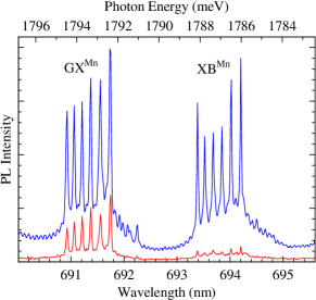
The sample offers a possibility to investigate and control an exciton coherence coupled, via ,- exchange interaction, with an individual spin of a magnetic dopantBesombes et al. (2004); Kudelski et al. (2007); Kobak et al. (2014); Smoleński et al. (2016); Lafuente-Sampietro et al. (2016); Fainblat et al. (2016). This is possible thanks to Mn -doping introduced within the CdTe QD layer. Via micro-photoluminescence spectroscopy we can recognize QDs containing Mn ions, and in particular distinguish those incorporating exactly one such dopant. To be more specific, QDs without magnetic ions exhibit sharp lines (typical full-width at half-maximum (FWHM) below 0.1 meV), originating from the exciton recombination. QDs with more than two magnetic ions exhibit spectrally broader lines (typically FWHM above 1 meV), which significantly shift in a magnetic field.Wojnar et al. (2007) For QDs with exactly two Mn ions, each excitonic transition gets split into a manifold of 36 lines, owing to 6*6 possible spin states of two Mn ions.Besombes et al. (2012) Finally, a spectral fingerprint of a QD with a single Mn ion is very characteristic: exciton transitions display 6-fold splitting, due to ,- exchange interaction with the Mn ion. The latter exhibits 6 possible spin states, corresponding to spin projection , , and on quantization axis of excitons (growth axis).Besombes et al. (2004) In our sample, majority of QDs do not contain Mn ions and thus show single lines. We have not observed QDs with two or more Mn ions. However, there is a small fraction (well below 1%) of QDs, which exhibit the PL pattern characteristic for QDs containing exactly one individual Mn ion. A typical example of PL measured at such magnetic QD is shown in Fig. 4: the excitonic spectral clusters corresponding to recombination of exciton-to-ground (GXMn) and biexciton-to-exciton states XBMn do display the characteristic 6-fold splitting Besombes et al. (2004). Spectra are measured as a function of the excitation power. As expected, the biexciton transitions exhibits a much stronger intensity dependence, than the exciton ones (see Fig. 4). Observation of a pronounced and spectrally sharp biexciton complex, with a binding energy of around 7 meV, indicates that QDs forming from fluctuations of thin CdTe layer in Cd0.77Zn0.13Mg0.10Te barrier are in fact well defined zero dimensional objects, which efficiently localize even four carriers (two holes and two electrons). Other excitonic complexes, corresponding to a negatively and/or positively charged QDs, doped with single Mn2+ ions have also been identified (not shown).
Four-wave mixing.
To retrieve the coherent nonlinear response of individual QDs, we employed the heterodyne spectral interferometry Langbein and Patton (2006). Technical details regarding the current implementation of the setup are provided in Ref. [Fras et al., 2016]. To resonantly excite the QDs at 680-690 nm with 0.3 ps pulses, we use an optical parametric oscillator (OPO model Inspire provided by Radiantis), pumped with a Ti:Sapphire laser (model Tsunami Femto provided by Spectra-Physics). The excitation spectrum generated by the OPO in shown in Fig. 5 b (green). We form a pair of pulse trains and with a variable delay controlled with a mechanical stage providing up to 1 ns. and are modulated using acousto-optic deflectors, optimized for a VIS range and driven at MHz and MHz, respectively. Both beams are recombined into the same spatial mode and are focussed to the diffraction limit at the sample surface using a microscope objective (NA=0.65) installed on a XYZ piezo-stage. We interfere the reflectance with the frequency shifted reference beam . In particular, by selecting the heterodyne mixing at MHz, we select the beating frequency corresponding to the FWM field, proportional to in the lowest order. The FWM- interference is spectrally resolved and detected by a CCD camera.
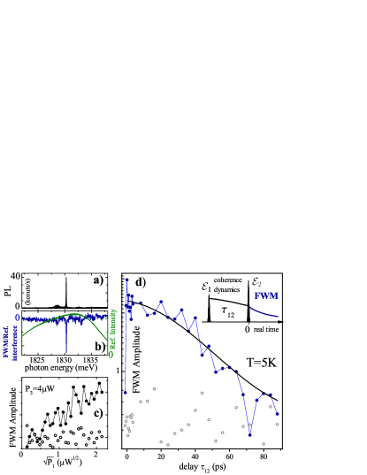
As candidates for FWM measurements, we pick up the transitions as the one shown in Fig. 5 a, which feature an enhanced flux of the PL, thus indicating an increased extraction efficiency with respect to other QDs. By monitoring the reflectance, we assure that the targeted transition lies at the minimum of the cavity mode. As a result, we expect the weak FWM field to be enhanced by a factor with respect to bare QDs, and thus capable to be induced with a respectively lowered resonant intensity of and .
A representative example of the FWM interference at ps is presented in Fig. 5, with a signal-to-noise of 10 after 300 s integration. This is comparable with previous FWM measurements on single QDs employing AR structures Patton et al. (2006); Kasprzak et al. (2013). In Fig. 5 c we present FWM amplitude, as a function of amplitude, proportional to its area . With increasing the latter, the FWM is expected to yield Rabi oscillations Fras et al. (2016), with the first maximum (minimum) at . In our case however, the accessible range of intensities is not sufficient to attain significant , so as to approach area. The flopping is not observed and we remain in the driving regime of the FWM.
In the inset of Fig. 5 d we illustrate the two-pulse sequence performed to infer the coherence dynamics of the same transition ( is set fixed, 1 ps prior to ): induces the coherence, which is converted into the density grating by . The latter is then self-diffracted into the FWM polarization. By measuring FWM as a function of one can access the homogeneous broadening (where denotes dephasing time) within the inhomogeneously broadened distribution via inferring photon echoes, which in case of a single QD are created by a random spectral wandering Patton et al. (2006); Kasprzak et al. (2013). The data are fit by the model including both homogeneous and inhomogeneous contributions to the spectral shape Kasprzak et al. (2013); Mermillod et al. (2016). The result, shown with a black trace, yields the dephasing time of ps and inhomogeneous broadening of eV (FWHM). A large uncertainty of stems from a limited range of the accessible delays, restricted by the time-resolution of the spectrometer - the issue which could be overcome by introducing the delay between and .Jakubczyk et al. (2016) Note the decrease of the FWM during initial several ps, which is due to dephasing with acoustic phonons.Jakubczyk et al. (2016) We observe no FWM signal for , which could rise from a two-photon coherence Mermillod et al. (2016) between the ground state and a two-exciton (biexciton) state in a QD. The missing signal for , indicates that the QD is charged, allowing only for the trion transition Fras et al. (2016). Finally, it is worth to point out an order of magnitude longer , with respect to the previous, and until now sole report available for the CdTe-platform Patton et al. (2006).
IV Discussion and conclusions
Our structure represents the third successful approach to the growth of photonic structures with QDs containing single Mn ions. The first report has been presented in Ref. [Pacuski et al., 2014], where a three-step process, involving two remote MBE facilities, was established to grow ZnTe/MgTe/MgSe based microcavities with CdTe/ZnTe QDs containing single Mn ions. In that case, growth interruptions were due to missing molecular sources in growth chambers: the first growth chamber was used to realize DBRs, the second one was employed for the growth of Mn-doped QDs. Recently, the same material system was used for the growth of Mn-doped QDs on the top of 10 DBR pairs. The process was carried out using a single MBE machine, but growth interruptions were anyway required to clean the chamber from the residual Se atoms, which incorporated into QDs and impaired their optical properties Rousset et al. (2016).
Comparing to previous works, here the procedure is significantly simplified, since Se is not involved in the growth of our microcavity based on (Cd,Zn,Mg)Te. Therefore, the whole process is realized in a single growth chamber, without growth interruptions. It can be reproduced in any MBE growth chamber devoted to Te compounds. One more important advantage of the present system is that CdTe /Cd0.77Zn0.13Mg0.10Te QDs with single Mn ion presented here could be brought toward the spectral range of Al2O3:Ti tunable femtosecond laser, i.e. above 700 nm. This could be particularly handy as it eliminates the requirement of using OPO sources to perform resonant, ultrafast spectroscopy of this material system. Finally, the design of antireflective photonic structure presented in this work will be necessary for achieving a satisfactory retrieval sensitivity of coherent nonlinear responses of magnetic QDs, where the exciton oscillator strength is distributed over a set of spin-assisted transitions.
V Acknowledgments
This work was partially supported by the ministry of science and higher education under grants Iuventus Plus IP2014 040473 and IP2014 034573, and by the Polish National Science Centre under decisions DEC-2015/18/E/ST3/00559, DEC-2011/02/A/ST3/00131, DEC-2014/13/N/ST3/03763, DEC-2013/09/B/ST3/02603, DEC-2015/16/T/ST3/00506, UMO-2012/05/B/ST7/02155. The research was carried out with the use of CePT, CeZaMat and NLTK infrastructures financed by the European Union - the European Regional Development Fund within the Operational Programme ”Innovative economy”. VD, TJ and JK acknowledge the financial support by the European Research Council (ERC) Starting Grant PICSEN (grant no. 306387).
References
- Wang (1974) Wang, S. IEEE Journal of Quantum Electronics 1974, 10, 413–427.
- Sadowski et al. (1997) Sadowski, J.; Mariette, H.; Wasiela, A.; André, R.; Merle d’Aubigné, Y.; Dietl, T. Phys. Rev. B 1997, 56, R1664–R1667.
- Benisty et al. (1998) Benisty, H.; De Neve, H.; Weisbuch, C. IEEE J. Quant. Electron. 1998, 34, 1612–1631.
- Ng et al. (1999) Ng, H. M.; Doppalapudi, D.; Iliopoulos, E.; Moustakas, T. D. Appl. Phys. Lett. 1999, 74, 1036–1038.
- Tawara et al. (2000) Tawara, T.; Yoshida, H.; Yogo, T.; Tanaka, S.; Suemune, I. J. Cryst. Growth 2000, 221, 699 – 703.
- Guo et al. (2000) Guo, S. P.; Maksimov, O.; Tamargo, M. C.; Peiris, F. C.; Furdyna, J. K. Appl. Phys. Lett. 2000, 77, 4107–4109.
- Pacuski et al. (2009) Pacuski, W.; Kruse, C.; Figge, S.; Hommel, D. Appl. Phys. Lett. 2009, 94, 191108.
- Gust et al. (2009) Gust, A.; Kruse, C.; Otte, K.; Kalden, J.; Meeser, T.; Sebald, K.; Gutowski, J.; Hommel, D. Nanotechnology 2009, 20, 015401.
- Rousset et al. (2013) Rousset, J.-G.; Kobak, J.; Slupinski, T.; Jakubczyk, T.; Stawicki, P.; Janik, E.; Tokarczyk, M.; Kowalski, G.; Nawrocki, M.; Pacuski, W. J. Cryst. Growth 2013, 378, 266 – 269.
- Koba and Suffczyński (2013) Koba, M.; Suffczyński, J. J. Electromagnet. Wave 2013, 27, 700–706.
- Koba and Suffczyński (2014) Koba, M.; Suffczyński, J. Europhys. Lett. 2014, 108, 27004.
- Jakubczyk et al. (2014) Jakubczyk, T.; Franke, H.; Smoleński, T.; Ściesiek, M.; Pacuski, W.; Golnik, A.; Schmidt-Grund, R.; Grundmann, M.; Kruse, C.; Hommel, D.; Kossacki, P. ACS Nano 2014, 8, 9970–9978.
- Schubert et al. (2008) Schubert, M. F.; Mont, F. W.; Chhajed, S.; Poxson, D. J.; Kim, J. K.; Schubert, E. F. Opt. Express 2008, 16, 5290–5298.
- Chhajed et al. (2008) Chhajed, S.; Schubert, M. F.; Kim, J. K.; Schubert, E. F. Appl. Phys. Lett. 2008, 93, 251108.
- Langbein and Patton (2006) Langbein, W.; Patton, B. Opt. Lett. 2006, 31, 1151–1153.
- Patton et al. (2006) Patton, B.; Langbein, W.; Woggon, U.; Maingault, L.; Mariette, H. Phys. Rev. B 2006, 73, 235354.
- Kasprzak et al. (2013) Kasprzak, J.; Portolan, S.; Rastelli, A.; Wang, L.; Plumhof, J. D.; Schmidt, O. G.; Langbein, W. New J. Phys. 2013, 15, 055006.
- Kasprzak et al. (2010) Kasprzak, J.; Reitzenstein, S.; Muljarov, E. A.; Kistner, C.; Schneider, C.; Strauss, M.; Höfling, S.; Forchel, A.; Langbein, W. Nat. Mater. 2010, 9, 304–308.
- Fras et al. (2016) Fras, F.; Mermillod, Q.; Nogues, G.; Hoarau, C.; Schneider, C.; Kamp, M.; Höfling, S.; Langbein, W.; Kasprzak, J. Nat. Photon. 2016, 10, 155–158.
- Mermillod et al. (2016) Mermillod, Q.; Jakubczyk, T.; Delmonte, V.; Delga, A.; Peinke, E.; Gérard, J.-M.; Claudon, J.; Kasprzak, J. Phys. Rev. Lett. 2016, 116, 163903.
- Rousset et al. (2015) Rousset, J.-G.; Piȩtka, B.; Król, M.; Mirek, R.; Lekenta, K.; Szczytko, J.; Borysiuk, J.; Suffczyński, J.; Kazimierczuk, T.; Goryca, M.; Smoleński, T.; Kossacki, P.; Nawrocki, M.; Pacuski, W. Appl. Phys. Lett. 2015, 107, 201109.
- Mirek et al. (2017) Mirek, R.; Król, M.; Lekenta, K.; Rousset, J.-G.; Nawrocki, M.; Kulczykowski, M.; Matuszewski, M.; Szczytko, J.; Pacuski, W.; Piȩtka, B. Phys. Rev. B 2017, 95, 085429.
- Gaj and Kossut (2011) Gaj, J. A.; Kossut, J. Introduction to the Physics of Diluted Magnetic Semiconductors; Springer Science & Business Media, 2011; Vol. 144.
- Besombes and Boukari (2014) Besombes, L.; Boukari, H. Phys. Rev. B 2014, 89, 085315.
- Sawicki et al. (2015) Sawicki, K.; Malinowski, F. K.; Gałkowski, K.; Jakubczyk, T.; Kossacki, P.; Pacuski, W.; Suffczyński, J. Appl. Phys. Lett. 2015, 106, 012101.
- Besombes et al. (2004) Besombes, L.; Léger, Y.; Maingault, L.; Ferrand, D.; Mariette, H.; Cibert, J. Phys. Rev. Lett. 2004, 93, 207403.
- Kudelski et al. (2007) Kudelski, A.; Lemaître, A.; Miard, A.; Voisin, P.; Graham, T. C. M.; Warburton, R. J.; Krebs, O. Phys. Rev. Lett. 2007, 99, 247209.
- Kobak et al. (2014) Kobak, J.; Smoleński, T.; Goryca, M.; Papaj, M.; Gietka, K.; Bogucki, A.; Koperski, M.; Rousset, J.-G.; Suffczyński, J.; Janik, E.; Nawrocki, M.; Golnik, A.; Kossacki, P.; Pacuski, W. Nat. Commun. 2014, 5, 3191.
- Smoleński et al. (2016) Smoleński, T.; Kazimierczuk, T.; Kobak, J.; Goryca, M.; Golnik, A.; Kossacki, P.; Pacuski, W. Nat. Commun. 2016, 7, 10484.
- Lafuente-Sampietro et al. (2016) Lafuente-Sampietro, A.; Utsumi, H.; Boukari, H.; Kuroda, S.; Besombes, L. Phys. Rev. B 2016, 93, 161301.
- Fainblat et al. (2016) Fainblat, R.; Barrows, C. J.; Hopmann, E.; Siebeneicher, S.; Vlaskin, V. A.; Gamelin, D. R.; Bacher, G. Nano Lett. 2016, 16, 6371–6377.
- Wojnar et al. (2007) Wojnar, P.; Suffczyński, J.; Kowalik, K.; Golnik, A.; Karczewski, G.; Kossut, J. Phys. Rev. B 2007, 75, 155301.
- Besombes et al. (2012) Besombes, L.; Cao, C. L.; Jamet, S.; Boukari, H.; Fernández-Rossier, J. Phys. Rev. B 2012, 86, 165306.
- Jakubczyk et al. (2016) Jakubczyk, T.; Delmonte, V.; Fischbach, S.; Wigger, D.; Reiter, D. E.; Mermillod, Q.; Schnauber, P.; Kaganskiy, A.; Schulze, J.-H.; Strittmatter, A.; Rodt, S.; Langbein, W.; Kuhn, T.; Reitzenstein, S.; Kasprzak, J. ACS Photonics 2016, 3, 2461–2466.
- Pacuski et al. (2014) Pacuski, W.; Jakubczyk, T.; Kruse, C.; Kobak, J.; Kazimierczuk, T.; Goryca, M.; Golnik, A.; Kossacki, P.; Wiater, M.; Wojnar, P.; Karczewski, G.; Wojtowicz, T.; Hommel, D. Cryst. Growth Des. 2014, 14, 988–992.
- Rousset et al. (2016) Rousset, J.-G.; Kobak, J.; Janik, E.; Parlinska-Wojtan, M.; Slupinski, T.; Golnik, A.; Kossacki, P.; Nawrocki, M.; Pacuski, W. J. Appl. Phys. 2016, 119, 183105.