Anisotropic plasmons, excitons and electron energy loss spectroscopy of phosphorene
Abstract
In this article, we explore the anisotropic electron energy loss spectrum (EELS) in monolayer phosphorene based on ab-initio time dependent density functional theory calculations. Similar to black phosphorous, the EELS of undoped monolayer phosphorene is characterized by anisotropic excitonic peaks for energies in vicinity of the bandgap, and by interband plasmon peaks for higher energies. On doping, an additional intraband plasmon peak also appears for energies within the bandgap. Similar to other two dimensional systems, the intraband plasmon peak disperses as in both the zigzag and armchair directions in the long wavelength limit, and deviates for larger wavevectors. The anisotropy of the long wavelength plasmon intraband dispersion is found to be inversely proportional to the square root of the ratio of the effective masses: .
I Introduction
Within the family of 2D materialsGeim and Novoselov (2007); Schwierz (2010); Radisavljevic et al. (2011); et.al (2013); Dubertret et al. (2015); Liu et al. (2014a); Li et al. (2014a); Ghosh et al. (2015); Novoselov et al. (2016); Nahas et al. (2016); Mardanya et al. (2016), phosphorene (few layers of black phosphorous) - a direct bandgap semiconductor with a puckered atomic structure, has a highly anisotropic band-structure Li et al. (2014b); Liu et al. (2014b); Ling et al. (2015). It has a massive Dirac like energy dispersion along the armchair and a parabolic Schrödinger like energy dispersion along the zigzag directionQiao et al. (2014); Rodin et al. (2014a); Rudenko and Katsnelson (2014a); Ezawa (2014a). This results in highly anisotropic single particle electronicQiao et al. (2014), thermalLiu and Chang (2015), many particle excitonicTran et al. (2014) and plasmonic properties Low et al. (2014). In particular, the plasmon dispersion has been recently calculated based on low energy continuum Hamiltonian, and it is found to be highly anisotropicLow et al. (2014); Rodin and Castro Neto (2015) with different doping dependence in different directions, depending on the number of layers.
From an experimental viewpoint, momentum resolved electron energy loss spectroscopyEgerton (2009) (EELS) directly probes the loss function of a material, which in turn is simply the inverse of the imaginary part of the dynamical interacting dielectric constant of a material: . It has been used extensively in a variety of materials such as grapheneEberlein et al. (2008); Shin et al. (2011); Kinyanjui, M. K. et al. (2012); Tegenkamp et al. (2011); Langer et al. (2010); Liou et al. (2015); et.al (2008); Yan et al. (2011), transition metal dichalcogenides et.al (2011); Johari and Shenoy (2011a), and bulk black phosphorousSchuster et al. (2015), to explore the single particle and collective excitations such as excitons and plasmons. In terms of computational methods, calculations based on effective low energy continuum Wunsch et al. (2006); Sachdeva et al. (2015) as well as the tight-binding Hamiltonian Hill et al. (2009); Lam and Guo (2015); Jin et al. (2015) are very insightful, but they fail to capture many of the experimental aspects of the EELS spectrum accurately; in particular the low energy intraband plasmons at large wave-vectors and the high energy interband plasmons involving transitions across various energy bands. For example, in doped graphene, the low energyWunsch et al. (2006); Hwang and Das Sarma (2007); Agarwal and Vignale (2015) and tight-binding approachHill et al. (2009) fails to capture the plasmon anisotropy at finite wave-vectors in the and the direction, which has been observed experimentally Tegenkamp et al. (2011); Langer et al. (2010). However, the loss function and corresponding plasmon dispersion relation is generally well described by density functional theory based ab-initio calculations Andersen and Thygesen (2013); Vacacela Gomez et al. (2016); Johari and Shenoy (2011b); Despoja et al. (2013); Kaltenborn and Schneider (2013); Andersen et al. (2014); Trevisanutto et al. (2008); Yan et al. (2011). In case of phosphorene, the low energy intraband plasmon spectrum has been studied using the continuum approximation Low et al. (2014); Rodin and Castro Neto (2015). Further, the effects of strainLam and Guo (2015) and disorderJin et al. (2015) on the plasmon spectrum have been incorporated using a tight-binding approach, but to the best of our knowledge, there is no ab-initio based study of the anisotropic plasmon dispersion (both low as well as high energy) and the high energy EELS spectrum of monolayer phosphorene. Motivated by this, we present an ab-initio density functional theory (DFT) based study of the anisotropic EELS spectrum, which includes low energy intraband plasmons at finite doping, excitons and interband plasmons in monolayer phosphorene.
We find that the crystal anisotropy of bulk black phosphorous is preserved down to it’s single layer, leading to a highly anisotropic electronic band structure, which results in a direction dependent EELS. In case of finite doping, we find an intraband plasmon mode which lies well below the band gap of phosphorene. Interestingly, it has a dispersion for small wave vector in each of the two principal direction (parallel to the armchair and the zigzag edge of monolayer phosphorene), which signifies the two dimensional nature of the plasmon mode. We also find a highly dispersive mode in the EELS, which appears at slightly higher energy than the bandgap of phosphorene; it is identified as the exciton peak. Interestingly, while the exciton peak appears in the armchair direction, it is completely absent along the zigzag edge. The other high energy peaks correspond to different interband transitions, with a very distinct peak appearing for energies close to eV. We also observe a general trend that with increasing momentum transfer, all the resonant features (excitations) of the EELS spectrum are blue shifted and they gradually loose their strength.
The paper is organized as follows: in Sec. II we discuss the formulation for calculating the interacting density response function and the corresponding EELS spectrum, along with the computational details of our ab-initio study to get the electronic band structure of phosphorene. Next, we describe the calculated EELS spectrum in Sec. III, followed by a detailed discussion focused on anisotropy of intraband plasmons in Sec. IV. Finally, we summarize our findings in Sec. V.
II Theory and Computational details
II.1 Dynamical dielectric and loss function
Our starting point is the non-interacting density-density response function for a periodic lattice, which is obtained from the Adler-Wiser formula given byAdler (1962); Wiser (1963),
| (1) | |||
The Kohn-Sham energy eigenvalues ,the wave function and the corresponding Fermi-Dirac occupation function for the nth band at wave vector are obtained from the ground state calculations performed using the density functional theory.
Within the framework of time dependent density functional theory (TDDFT) the interacting density-density response function can be obtained by solving a Dyson-type equation. Expanding in a plane wave basis (valid for a periodic system), the interacting response function can be expressed as
where and are the reciprocal lattice vector and the wave vector, respectively and is the (2D truncated for monolayer phosphorene) Coulomb kernel. The exchange-correlation part of the kernel is neglected within the framework of the random phase approximation (RPA). Using the matrix, the macroscopic dielectric function () is obtained as,
| (3) |
where is the (2D truncated for monolayer phosphorene) Coulomb Kernel as described in Ref. [Rozzi et al., 2006]. The dynamical loss function, which is directly related to the EELS, is calculated as
| (4) |
Plasmons (collective density excitations) are the characterized by the zeroes of the real part of the macroscopic dielectric function (the denominator of the density-density response function within RPA).
II.2 Computational details
Electronic band structure calculations are performed using density functional theory, as implemented in the GPAW package Mortensen et al. (2005); et.al (2010); Bahn and Jacobsen (2002). The kinetic energy cut-off for the plane wave basis set is taken to be 500 eV. Initially, all the atomic positions are relaxed (using GGA) until the forces on each atom are less than 0.001 eV/Å. Next, we calculate the single particle states [to be used as input for evaluating the response function in Eq. (1)] using the GLLB-SC functional which includes the GLLB type exchange proposed by Gritsenko et al. and PBEsol correlation, which has been found to improve the bandgap in case of semiconductorsGritsenko et al. (1995). While a k-point grid of ( ) is used for the Brillouin zone integrations of the bulk (monolayer) structure, for the electronic band structure calculation, a much denser k-point grid of 32 44 14 ( 64 88 1) is used for calculating the dependence of the EELS, giving a momentum resolution of 0.043 Å-1 and 0.0215 Å-1 respectively for the bulk and the monolayer phosphorene. In case of the latter, we use a vacuum layer of 20 Å in the direction perpendicular to the phosphorene plane to suppress any interaction between two replica images in the vertical direction.
EELS calculations are performed using the generalized random phase approximation (RPA). The generalized RPA uses the local field factors to add the impact of the exchange and correlation effects to the Hartree field Giuliani and Vignale (2005). Because of it’s long-range nature, the Coulomb potential of one layer can interact with its periodic replicas, which is avoided by taking a 2D truncated Coulomb kernel, following Ref [Rozzi et al., 2006]. We consider up to 50 empty bands to correctly describe all the electronic excitations. For the local field corrections, a cut-off energy of 50 eV is used for G and vectors, which corresponds to 259 (135) plane waves for monolayer phosphorene (bulk black phsophorous). Doping or the change in carrier concentration is achieved by shifting the position of the Fermi energy ().
II.3 Electronic band structure of phosphorene
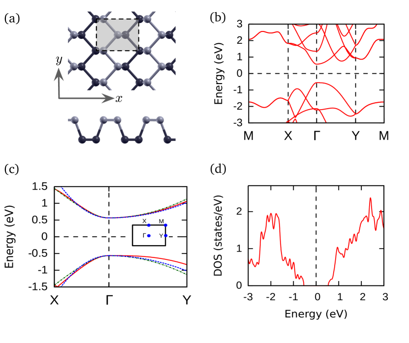
Phosphorene has a layered structure with each phosphorus atom covalently bonded with three adjacent atoms, forming a hybridized puckered honeycomb structure [see Fig 1(a)]. As shown in the figure, mutually perpendicular armchair and zigzag directions are aligned along the and axis, respectively. The lattice parameters of the bulk unit cell are found to be Å (armchair), Å (zigzag) and Å, which are in good agreement with the values reported in the literatureLiu et al. (2014b). As shown in Fig 1(a), and are the high symmetry directions in the reciprocal lattice, which are aligned along the armchair and zigzag axes, respectively. Based on previous reports of large anisotropy of calculated and measured electronic and optical properties along these particular directions, in this paper we calculate and compare the EELS spectrum and the intraband low energy plasmon dispersion along and , respectively.
As reported in the literature, monolayer phosphorene is found to be a direct bandgap semiconductor, the magnitude of the gap being 1.51 eV (0.91 eV), calculated using the HSE06 (GGA-PBE) functional Qiao et al. (2014); Kumar et al. (2016); Ghosh et al. (2016). The GLLB-SC computed electronic bandstructure has a direct bandgap of 1.13 eV and it is shown in Fig 1, along with the corresponding density of states (DOS). The conduction band minima (CBM) and the valance band maxima (VBM) are located at the -point. Interestingly, the electron dispersion is anisotropic and ‘semi-Dirac’ like around this point [see Fig 1(b)], having a massive Dirac character along the direction and parabolic with a large effective mass along the direction De Sarkar et al. (2016). This highly anisotropic low energy dispersion of phosphrene is the origin of the direction dependent transport and optical properties of phosphorene.
Pristine phosphorene, being a relatively large bandgap semiconductor, has vanishingly small thermally excited charge carriers even at room temperature and consequently intraband plasmons are absent. In order to explore intraband plasmons we consider phosphorene doped via electrostatic doping (controlled by a varying gate voltage). For electrostatic doping, the bands near the CBM (and thus the DOS) remains unaffected but the Fermi energy shifts to the conduction band giving rise to doped (electronic) charge carriers, whose number density can be tuned by controlling the gate voltage.
The effective low energy Hamiltonian and band-structure of monolayer phosphorene has been derived using methodRodin et al. (2014b) as well as the tight-binding approach Rudenko and Katsnelson (2014b); Rudenko et al. (2015); Ezawa (2014b); Pereira and Katsnelson (2015), both of which yield a qualitatively similar picture De Sarkar et al. (2016). For this manuscript we work with the bare minimum effective low energy Hamiltonian of phosphorene, retaining only the lowest order terms in the wavevectors Ezawa (2015),
| (5) |
where ’s are the Pauli matrices. The anisotropic energy spectrum is thus given by
| (6) |
where corresponds to the conduction (valance) band. Fitting Eq. (6) to our GLLB-SC dispersion in vicinity of the point [see Fig. 1(c)] yields eV, eV/Å2 and eV/Å. Note that, Eq. (6) can further be approximated as an anisotropic parabolic dispersion given by
| (7) |
where . The values of the anisotropic effective masses for the conduction band are given by and , with being the electrons rest mass, consistent with earlier studies Qiao et al. (2014). Equations (5)-(6) will be used to obtain the low energy and low momentum transfer plasmon dispersion of monolayer phosphorene analytically which in turn will be compared with our ab-initio results.
III Electron energy loss spectrum
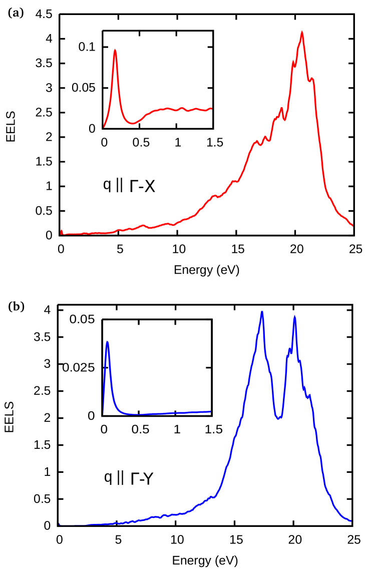
Having discussed the ab-initio and the low energy electronic band structure, we now proceed to calculate the EELS spectrum of phosphorene. We first test the methodology by calculating the EELS spectrum of bulk black phosphorous and comparing the same with reported data Schuster et al. (2015); Wu et al. (2015). The computed EELS spectrum of bulk black phosphorous is shown in Fig. 2. As expected, the anisotropic nature of the electronic bandstructure of bulk phosphorous is manifested in the EELS data. The high energy interband plasmon peak, present in the vicinity of 20 eV in both the and the direction, is in good agreement with the recently published experimental EELS results for bulk black phosphorous Wu et al. (2015). The low energy part of the spectrum, representing intraband plasmons and excitons, are shown in the inset of Fig. 2, and a marked anisotropy along the two principal direction is observed. In particular, the low energy exciton peak in black phosphorous ( eV) is only present in the (armchair) direction, which is consistent with recently reported measurements Schuster et al. (2015). Also, the intraband plasmons in the armchair direction () have a higher intensity as opposed to those in the zigzag () direction.
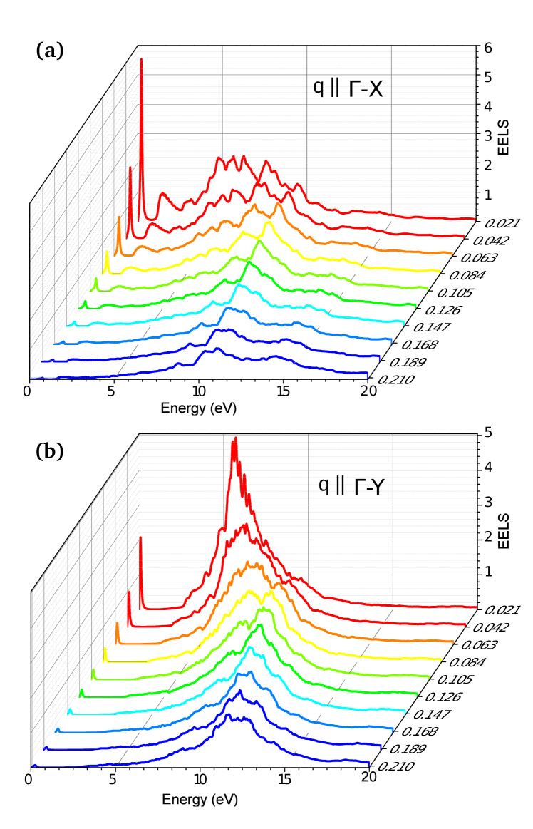
After benchmarking the methodology by successfully reproducing the characteristic features of EELS of bulk black phosphorus, next we focus on monolayer phosphorene. Due to obvious reasons related to it’s electronic band structure [see Fig 1 (b)], EELS of monolayer phosphorene is also found to be highly anisotropic. This can clearly be observed in Fig. 3(a) and (b), where the calculated spectrum of a single layer of doped (by taking meV, measured from the CBM) phosphorene is plotted for momentum transfer () along the (armchair) and (zigzag) directions, respectively. Note that, while the lowest energy peak due to the intraband plasmons are observed only in case of finite doping, others appearing at higher energy have intrinsic origin related to excitons and interband plasmons and they are present in undoped phosphorene as well. Specific features of the EELS are discussed in detail in the following subsections.
III.1 Intraband plasmons
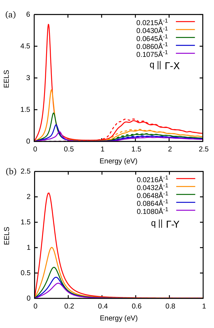
As shown in Fig. 3 and Fig. 4, the first peak appears for energies less than 0.25 eV. The energy corresponding to the peak is well below the bandgap of the pristine monolayer phosphorene and in addition this peak is absent in case of undoped phosphorene. Thus we interpret this as the peak originating from the intraband plasmon modes. With increasing momentum transfer, the intensity of intraband plasmons decreases and the peak position shifts to a higher energy, in both and direction [see Fig. 3 and Fig. 4]. Similar type of blue shift is observed as the doping is increased. Alike bulk black phsophorous, the intensity of the intraband peak is lower for momentum transfer along the direction, than compared to the direction, which has the maximum intensity among all the EELS peaks at [see Fig. 3]. The anisotropy of intraband plasmon modes and their momentum and doping dependence are discussed in detail in Sec. IV.
III.2 Low energy excitons
The next peak in the EELS is observed in the vicinity of eV, which is gradually shifted towards the higher energy, accompanied by intensity reduction with increasing . Note that, this peak is much more dispersive compared to the intraband plasmon peaks and extends approximately upto 3 eV (see Fig. 3 and Fig. 4). Since the peak energy coincides approximately with the energy gap of monolayer phosphorene and it exists in undoped phosphorene as well and it is almost independent of doping, we identify this as the lowest energy excitonic peak. As shown in Fig. 3 and Fig. 4, the excitonic peak is highly anisotropic in nature, as it appears only in case of momentum transfer along the direction, while being completely absent along the . We believe that the strongly anisotropic optical response reported for monolayer black phsophorene, which is transparent to the incident light in the energy range of 1.1-2.5 eV, but only if it is polarized along the zigzag direction and opaque if the light is polarized in the armchair directionTran et al. (2014); Schuster et al. (2015), originates from the anisotropy of the lowest energy electron-hole pair excitation observed in this work. Note that, since the crystal anisotropy observed in monolayer persists for multilayer, as well as bulk black phosphorous, similar kind of anisotropic excitonic response is expected at higher thickness as well.
III.3 Interband high energy plasmons
As we move towards higher energy, the next prominent EELS peak appears in the vicinity of eV, and similar to the low energy peaks, it’s intensity reduces accompanied by a blue shift with increasing momentum transfer. Though it is also anisotropic in nature, this peak has a higher intensity along the zigzag direction as compared to the armchair direction – unlike the case of intraband plasomons. As expected, this high energy peak is nearly independent of doping, as it corresponds to very high energy interband transitions.
Comparing the EELS intensity of various peaks as a function of , it is clear that in general the EELS intensity is maximum for direct transitions with and decays with increasing . However, the low energy intraband plasmon peak decays more rapidly with increasing (on account of damping by electron-hole excitations) as compared to the high energy peaks associated with interband transitions. For example, in case of , the intraband plasmon peak is the most intense one among all the EELS peaks for Å-1), which almost vanishes at higher , leaving the interband transition peak around 10-14 eV to be the most prominent one. Owing to it’s anisotropic nature, the scenario is different in case of , where the interband transition peak around 5 eV has the highest intensity (at Å-1) among all the EELS peaks and it broadens significantly and shifts to around 10-14 eV at higher value of .
Note that, other than the intraband plasmons, rest of the peaks corresponding to the interband transitions are likely to be affected due to the bandgap underestimation (approximately 40%) of GLLB-SC based electronic band structure calculations. For example, while the GW bandgap is reported to be 1.84 eVGhosh et al. (2016); Qiao et al. (2014) for monolayer black phosphorus, it is found to be 1.13 eV in our calculation. Thus, the EELS peaks corresponding to interband transitions are expected to be blue shifted in an actual experiment. However, the GLLB-SC bandgap estimation of eV for bulk black phosphorous is very close to its experimentally reported value of eV Ghosh et al. (2016). Thus it turns out that for bulk black phosphorous, EELS peak of 20 eV (as shown in Fig. 2) based on GLLB-SC calculations is consistent with the 20 eV peak observed in recent experimentsWu et al. (2015).
IV Anisotropic intraband plasmons
Having described the prominent features of the EELS spectrum of monolayer phosphorene, we now focus on the anisotropic nature of the low energy intraband plasmons and investigate their and doping () dependence. The low energy loss function along the and directions, is shown in Fig. 4 (a) and (b), respectively. As discussed earlier, the first low energy peak which appears for energies significantly below the bandgap of phosphorene and is only present in case of finite doping, corresponds to intraband plasmons - or collective charge density excitations. As shown in Fig 4, the intra-band plasmon peak has higher intensity along the direction as compared to the direction, similar to the case of bulk phosphorus. Interestingly, the intensity decay and blue shift of the intraband plasmon peak is more rapid in the direction, than compared to the direction.
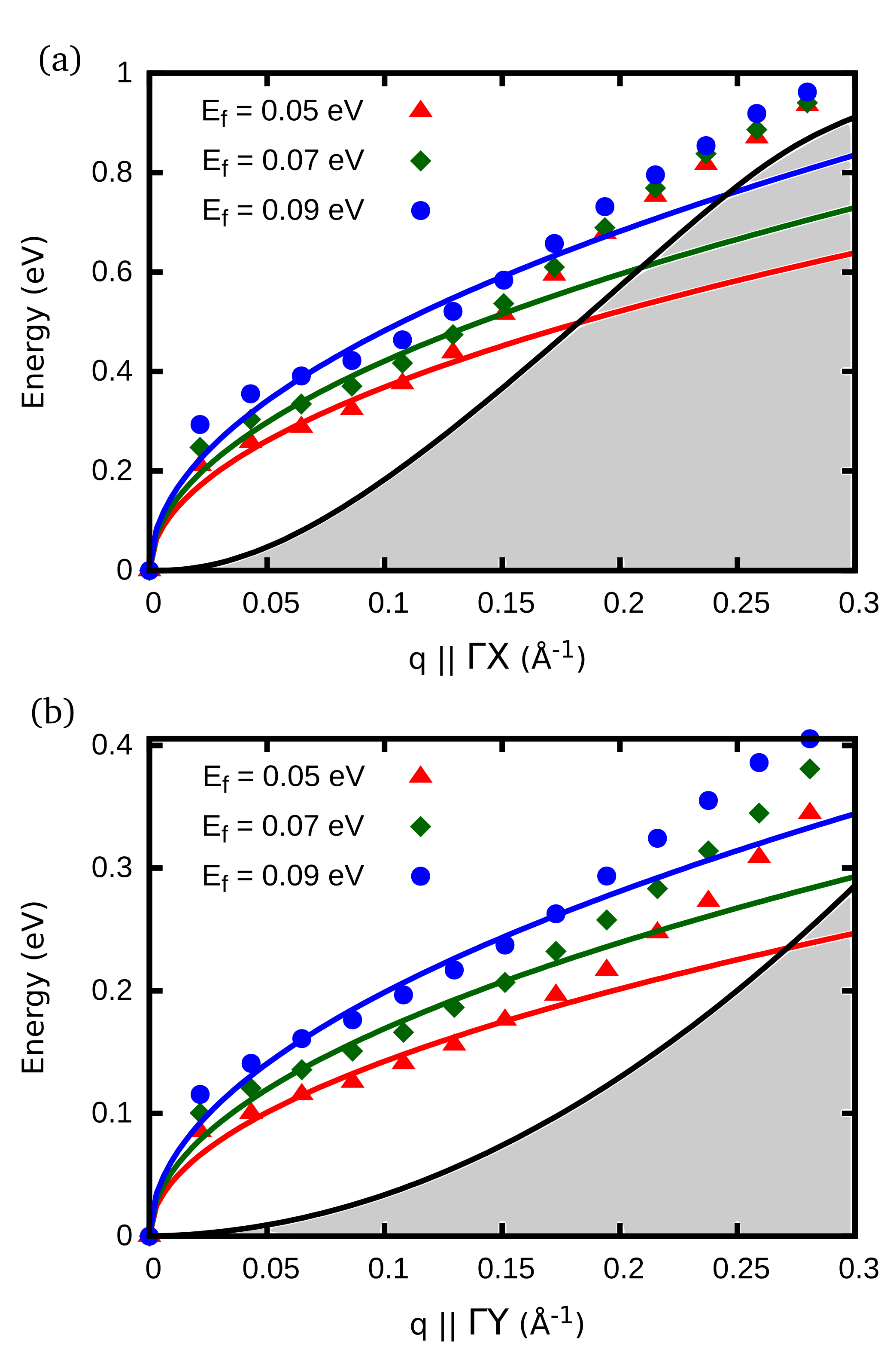
The momentum dependence of the intraband plasmon peak is further analyzed at different doping (by varying the Fermi energy) in Fig. 5. As shown in the figure, for relatively small momentum transfers, the dispersion follows the universal long wavelength behavior which is ubiquitous in two dimensional systems Sachdeva et al. (2015). For higher value of the momentum transfer , a clear deviation from the behavior is observed. Eventually the plasmon dissipates into single particle continuum of the conduction band, whose boundary is marked by the maxima of [see the shaded area in Fig. 5]. As shown in Fig. 5, increasing the doping extends the range of validity of behavior. For example, at meV the fit along the direction holds good upto Å-1, which extends upto Å-1 with increased doping ( meV). Similar behaviour of the plasmon dispersion is also seen along the direction, albeit the spectral weight of the corresponding plasmon peak is smaller in the direction.
Starting from the anisotropic parabolic approximation of the bandstructure of monolayer phosphorene, given by Eq. (7), the low energy plasmon dispersion within the random phase approximation, (for the Coulomb potential ) has been obtained in Ref. [Rodin and Castro Neto, 2015]. It is explicitly given by
| (8) |
where we have defined , , and is the two dimensional density of states for an anisotropic parabolic band system. Eq. (8) directly yields the following: 1) dependence of the plasmon dispersion in all directions for small wavevectors, 2) dependence of the low energy (and low wave-vector) plasmon dispersion on the Fermi energy, and 3) the long wave-length anisotropy of the plasmon dispersion , independent of the doping in the system.
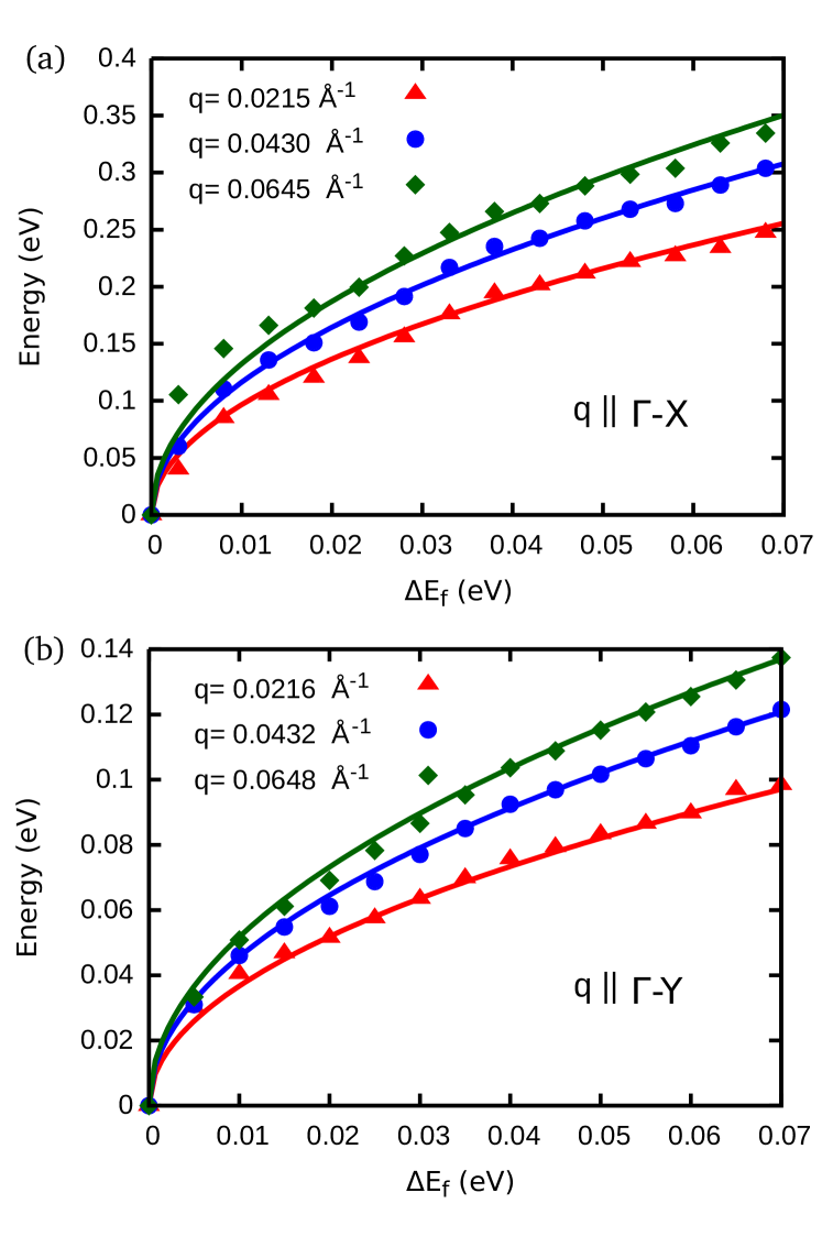
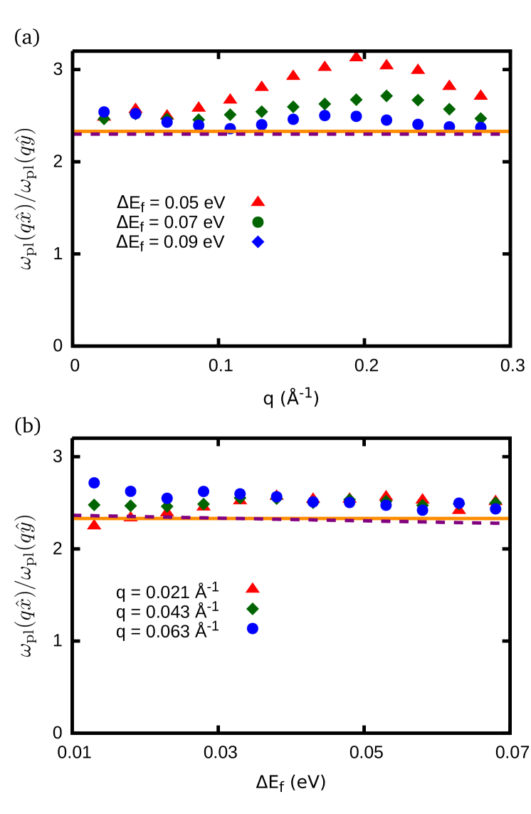
The doping dependence of the intraband plasmon dispersion is shown in Fig. 6, and it clearly shows a reasonable match of the plasmon dispersion with the expected dependence of the Fermi energy for small . The plasmon frequency anisotropy ratio is shown in Fig. 7 and it also seems to be more or less consistent with the behavior. A more thorough calculation of the long wavelength plasmon dispersion using the semi-Dirac continuum Hamiltonian for phosphorene (see Eq. (5)), is presented in the appendix, and it also yields qualitatively similar results. However, the anisotropy ratio now explicitly depends on the Fermi energy – see Eq. (18). However we note that this dependence of the anisotropic ratio of the plasmon frequency is small – as shown in panel b) of Fig. 7.
V Summary and conclusions
In this article we present a thorough study of the anisotropic EELS spectrum of monolayer phosphorene using the TDDFT framework. We find that the anisotropy of the underlaying phosphorene crystal leads to the anisotropy in the band structure and consequently in the EELS spectrum as well – similar to the case of bulk black phoophorous. For finite doping in the system, the lowest energy peak in the EELS corresponds to the intraband plasmon mode (charge density excitations) in the sub electron volt range. At slightly higher energy than the band gap, there is a highly dispersive low energy exciton mode, which is almost independent of the doping and it is absent for the momentum transfer along the direction. At even higher energies and completely independent of the doping, there are various plasmon modes arising from the interband transitions with a very distinct peak appearing at eV for monolayer phosphorene (as per GLLB calculations). With increasing number of phosphorene layers (or thickness) this mode is likely to shift to higher energies eventually merging into a 19 eV peak observed in the bulk black phosphorous. We explore the low energy anisotropic intraband plasmons in detail and compare their behavior to analytical expression of the corresponding plasmon dispersion arising from the effective low energy dispersion using RPA. The anisotropic intraband plasmon modes are found to be highly dispersive in nature, with the large wavelength limit following the behavior in all directions which is a universal characteristic of plasmons in two dimensions. With increasing doping, the long wavelength plasmon dispersion is found to scale with the Fermi energy as . The anisotropy of the long wavelength plasmon dispersion is found to be proportional to the ratio of square root of the effective masses: .
Acknowledgements
We acknowledge funding from the following DST (Department of science and technology, government of India) schemes: 1) DST INSPIRE Faculty Award, 2)SERB Fast Track Scheme for Young Scientist 3) Ramanujan Fellowship, and 3) DST Nanomission project. We also thank CC IITK for providing HPC facility.
Appendix A Low energy plasmon dispersion of phosphorene
Here we calculate the low energy plasmon dispersion for a massive semi Dirac system in two dimensions, described by Eq. (5). The polarization (density-density response) function is given by
where , , , is the overlap function of spinors and is the Fermi function. Expanding the polarization function defined in Eq. (A), upto and at zero temperature, leads to
where , and are complex functions defined as follows
| (11) | |||||
| (12) |
Performing the integral in Eq. (A) we obtain,
| (13) | |||||
where we have defined
| (14) |
Equation (A) in turn uses the following notation,
| (15) |
where and are incomplete elliptic integral of the first and second kind respectively.
Within RPA, the plasmons modes are given by the zeros of the longitudinal dielectric functions,
| (16) |
where is the Fourier transform of the Coulomb potential. Substituting Eq. (13) in Eq. (16) immediately yields the long wavelength plasmon dispersion to be
| (17) | |||||
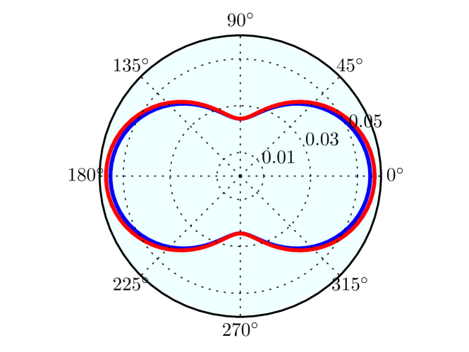
where we have used the two dimensional form of and defined . Figure 8, shows the angular dependence of the long wavelength plasmon frequency, specified by Eq. (17), and it matches reasonably well with the long wavelength expression given in Eq. (8).
The ratio of the anisotropic plasmon dispersion in and direction for same value of the wave vector (in the long wavelength regime) is given by
| (18) |
References
- Geim and Novoselov (2007) A. K. Geim and K. S. Novoselov, “The rise of graphene,” Nat Mater 6, 183–191 (2007).
- Schwierz (2010) Frank Schwierz, “Graphene transistors,” Nat. Nanotechnol. 5, 487–496 (2010).
- Radisavljevic et al. (2011) B Radisavljevic, Radenovic A, Brivio J, Giacometti V, and Kis A, “Single-layer mos2 transistors,” Nat. Nanotechnol. 6, 147–150 (2011).
- et.al (2013) Sheneve Z. Butler et.al, “Progress, challenges, and opportunities in two-dimensional materials beyond graphene,” ACS Nano 7, 2898–2926 (2013).
- Dubertret et al. (2015) Benoit Dubertret, Thomas Heine, and Mauricio Terrones, “The rise of two-dimensional materials,” Accounts of Chemical Research, Accounts of Chemical Research 48, 1–2 (2015).
- Liu et al. (2014a) Han Liu, Adam T. Neal, Zhen Zhu, Zhe Luo, Xianfan Xu, David Tománek, and Peide D. Ye, “Phosphorene: An unexplored 2d semiconductor with a high hole mobility,” ACS Nano 8, 4033–4041 (2014a).
- Li et al. (2014a) Likai Li, Yijun Yu, Guo Jun Ye, Qingqin Ge, Xuedong Ou, Hua Wu, Donglai Feng, Xian Hui Chen, and Yuanbo Zhang, “Black phosphorus field-effect transistors,” Nat. Nanotechnol. 9, 372–377 (2014a).
- Ghosh et al. (2015) Barun Ghosh, Suhas Nahas, Somnath Bhowmick, and Amit Agarwal, “Electric field induced gap modification in ultrathin blue phosphorus,” Phys. Rev. B 91, 115433 (2015).
- Novoselov et al. (2016) K. S. Novoselov, A. Mishchenko, A. Carvalho, and A. H. Castro Neto, “2d materials and van der waals heterostructures,” Science 353, 461 (2016).
- Nahas et al. (2016) Suhas Nahas, Barun Ghosh, Somnath Bhowmick, and Amit Agarwal, “First-principles cluster expansion study of functionalization of black phosphorene via fluorination and oxidation,” Phys. Rev. B 93, 165413 (2016).
- Mardanya et al. (2016) Sougata Mardanya, Vinay Kumar Thakur, Somnath Bhowmick, and Amit Agarwal, “Four allotropes of semiconducting layered arsenic that switch into a topological insulator via an electric field: Computational study,” Phys. Rev. B 94, 035423 (2016).
- Li et al. (2014b) Likai Li, Yijun Yu, Guo Jun Ye, Qingqin Ge, Xuedong Ou, Hua Wu, Donglai Feng, Xian Hui Chen, and Yuanbo Zhang, “Black phosphorus field-effect transistors,” Nat Nano 9, 372–377 (2014b).
- Liu et al. (2014b) Han Liu, Adam T. Neal, Zhen Zhu, Zhe Luo, Xianfan Xu, David Tománek, and Peide D. Ye, “Phosphorene: An unexplored 2d semiconductor with a high hole mobility,” ACS Nano 8, 4033–4041 (2014b).
- Ling et al. (2015) Xi Ling, Han Wang, Shengxi Huang, Fengnian Xia, and Mildred S. Dresselhaus, “The renaissance of black phosphorus,” Proceedings of the National Academy of Sciences 112, 4523–4530 (2015).
- Qiao et al. (2014) Jingsi Qiao, Xianghua Kong, Zhi-Xin Hu, Feng Yang, and Wei Ji, “High-mobility transport anisotropy and linear dichroism in few-layer black phosphorus,” Nat Commun 5 (2014).
- Rodin et al. (2014a) A. S. Rodin, A. Carvalho, and A. H. Castro Neto, “Strain-induced gap modification in black phosphorus,” Phys. Rev. Lett. 112, 176801 (2014a).
- Rudenko and Katsnelson (2014a) A. N. Rudenko and M. I. Katsnelson, “Quasiparticle band structure and tight-binding model for single- and bilayer black phosphorus,” Phys. Rev. B 89, 201408 (2014a).
- Ezawa (2014a) Motohiko Ezawa, “Topological origin of quasi-flat edge band in phosphorene,” New Journal of Physics 16, 115004 (2014a).
- Liu and Chang (2015) Te-Huan Liu and Chien-Cheng Chang, “Anisotropic thermal transport in phosphorene: effects of crystal orientation,” Nanoscale 7, 10648–10654 (2015).
- Tran et al. (2014) Vy Tran, Ryan Soklaski, Yufeng Liang, and Li Yang, “Layer-controlled band gap and anisotropic excitons in few-layer black phosphorus,” Phys. Rev. B 89, 235319 (2014).
- Low et al. (2014) Tony Low, Rafael Roldán, Han Wang, Fengnian Xia, Phaedon Avouris, Luis Martín Moreno, and Francisco Guinea, “Plasmons and screening in monolayer and multilayer black phosphorus,” Phys. Rev. Lett. 113, 106802 (2014).
- Rodin and Castro Neto (2015) A. S. Rodin and A. H. Castro Neto, “Collective modes in anisotropic double-layer systems,” Phys. Rev. B 91, 075422 (2015).
- Egerton (2009) R F Egerton, “Electron energy-loss spectroscopy in the tem,” Reports on Progress in Physics 72, 016502 (2009).
- Eberlein et al. (2008) T. Eberlein, U. Bangert, R. R. Nair, R. Jones, M. Gass, A. L. Bleloch, K. S. Novoselov, A. Geim, and P. R. Briddon, “Plasmon spectroscopy of free-standing graphene films,” Phys. Rev. B 77, 233406 (2008).
- Shin et al. (2011) S. Y. Shin, N. D. Kim, J. G. Kim, K. S. Kim, D. Y. Noh, Kwang S. Kim, and J. W. Chung, “Control of the π plasmon in a single layer graphene by charge doping,” Applied Physics Letters 99, 082110 (2011).
- Kinyanjui, M. K. et al. (2012) Kinyanjui, M. K., Kramberger, C., Pichler, T., Meyer, J. C., Wachsmuth, P., Benner, G., and Kaiser, U., “Direct probe of linearly dispersing 2d interband plasmons in a free-standing graphene monolayer,” EPL 97, 57005 (2012).
- Tegenkamp et al. (2011) C Tegenkamp, H Pfnür, T Langer, J Baringhaus, and H W Schumacher, “Plasmon electron–hole resonance in epitaxial graphene,” Journal of Physics: Condensed Matter 23, 012001 (2011).
- Langer et al. (2010) T Langer, J Baringhaus, H Pfnür, H W Schumacher, and C Tegenkamp, “Plasmon damping below the landau regime: the role of defects in epitaxial graphene,” New Journal of Physics 12, 033017 (2010).
- Liou et al. (2015) S. C. Liou, C.-S. Shie, C. H. Chen, R. Breitwieser, W. W. Pai, G. Y. Guo, and M.-W. Chu, “- plasmon dispersion in free-standing graphene by momentum-resolved electron energy-loss spectroscopy,” Phys. Rev. B 91, 045418 (2015).
- et.al (2008) C. Kramberger et.al, “Linear plasmon dispersion in single-wall carbon nanotubes and the collective excitation spectrum of graphene,” Phys. Rev. Lett. 100, 196803 (2008).
- Yan et al. (2011) Jun Yan, Kristian S. Thygesen, and Karsten W. Jacobsen, “Nonlocal screening of plasmons in graphene by semiconducting and metallic substrates: First-principles calculations,” Phys. Rev. Lett. 106, 146803 (2011).
- et.al (2011) Jonathan N. Coleman et.al, “Two-dimensional nanosheets produced by liquid exfoliation of layered materials,” Science 331, 568–571 (2011).
- Johari and Shenoy (2011a) Priya Johari and Vivek B. Shenoy, “Tunable dielectric properties of transition metal dichalcogenides,” ACS Nano 5, 5903–5908 (2011a).
- Schuster et al. (2015) R. Schuster, J. Trinckauf, C. Habenicht, M. Knupfer, and B. Büchner, “Anisotropic particle-hole excitations in black phosphorus,” Phys. Rev. Lett. 115, 026404 (2015).
- Wunsch et al. (2006) B Wunsch, T Stauber, F Sols, and F Guinea, “Dynamical polarization of graphene at finite doping,” New Journal of Physics 8, 318 (2006).
- Sachdeva et al. (2015) Rashi Sachdeva, Anmol Thakur, Giovanni Vignale, and Amit Agarwal, “Plasmon modes of a massive dirac plasma, and their superlattices,” Phys. Rev. B 91, 205426 (2015).
- Hill et al. (2009) A. Hill, S. A. Mikhailov, and K. Ziegler, “Dielectric function and plasmons in graphene,” EPL (Europhysics Letters) 87, 27005 (2009).
- Lam and Guo (2015) Kai-Tak Lam and Jing Guo, “Plasmonics in strained monolayer black phosphorus,” Journal of Applied Physics 117, 113105 (2015).
- Jin et al. (2015) Fengping Jin, Rafael Roldán, Mikhail I. Katsnelson, and Shengjun Yuan, “Screening and plasmons in pure and disordered single- and bilayer black phosphorus,” Phys. Rev. B 92, 115440 (2015).
- Hwang and Das Sarma (2007) E. H. Hwang and S. Das Sarma, “Dielectric function, screening, and plasmons in two-dimensional graphene,” Phys. Rev. B 75, 205418 (2007).
- Agarwal and Vignale (2015) Amit Agarwal and Giovanni Vignale, “Plasmons in spin-polarized graphene: A way to measure spin polarization,” Phys. Rev. B 91, 245407 (2015).
- Andersen and Thygesen (2013) Kirsten Andersen and Kristian S. Thygesen, “Plasmons in metallic monolayer and bilayer transition metal dichalcogenides,” Phys. Rev. B 88, 155128 (2013).
- Vacacela Gomez et al. (2016) C. Vacacela Gomez, M. Pisarra, M. Gravina, J. M. Pitarke, and A. Sindona, “Plasmon modes of graphene nanoribbons with periodic planar arrangements,” Phys. Rev. Lett. 117, 116801 (2016).
- Johari and Shenoy (2011b) Priya Johari and Vivek B. Shenoy, “Tunable dielectric properties of transition metal dichalcogenides,” ACS Nano, ACS Nano 5, 5903–5908 (2011b).
- Despoja et al. (2013) V. Despoja, D. Novko, K. Dekanić, M. Šunjić, and L. Marušić, “Two-dimensional and plasmon spectra in pristine and doped graphene,” Phys. Rev. B 87, 075447 (2013).
- Kaltenborn and Schneider (2013) Steffen Kaltenborn and Hans Christian Schneider, “Plasmon dispersions in simple metals and heusler compounds,” Phys. Rev. B 88, 045124 (2013).
- Andersen et al. (2014) Kirsten Andersen, Karsten W. Jacobsen, and Kristian S. Thygesen, “Plasmons on the edge of nanostructures,” Phys. Rev. B 90, 161410 (2014).
- Trevisanutto et al. (2008) Paolo E. Trevisanutto, Christine Giorgetti, Lucia Reining, Massimo Ladisa, and Valerio Olevano, “Ab Initio many-body effects in graphene,” Phys. Rev. Lett. 101, 226405 (2008).
- Adler (1962) Stephen L. Adler, “Quantum theory of the dielectric constant in real solids,” Phys. Rev. 126, 413–420 (1962).
- Wiser (1963) Nathan Wiser, “Dielectric constant with local field effects included,” Phys. Rev. 129, 62–69 (1963).
- Rozzi et al. (2006) Carlo A. Rozzi, Daniele Varsano, Andrea Marini, Eberhard K. U. Gross, and Angel Rubio, “Exact coulomb cutoff technique for supercell calculations,” Phys. Rev. B 73, 205119 (2006).
- Mortensen et al. (2005) J. J. Mortensen, L. B. Hansen, and K. W. Jacobsen, “Real-space grid implementation of the projector augmented wave method,” Phys. Rev. B 71, 035109 (2005).
- et.al (2010) J Enkovaara et.al, “Electronic structure calculations with gpaw: a real-space implementation of the projector augmented-wave method,” Journal of Physics: Condensed Matter 22, 253202 (2010).
- Bahn and Jacobsen (2002) S. R. Bahn and K. W. Jacobsen, “An object-oriented scripting interface to a legacy electronic structure code,” Comput. Sci. Eng. 4, 56–66 (2002).
- Gritsenko et al. (1995) Oleg Gritsenko, Robert van Leeuwen, Erik van Lenthe, and Evert Jan Baerends, “Self-consistent approximation to the kohn-sham exchange potential,” Phys. Rev. A 51, 1944–1954 (1995).
- Giuliani and Vignale (2005) G. Giuliani and G. Vignale, Quantum Theory of the Electron Liquid, Masters Series in Physics and Astronomy (Cambridge University Press, 2005).
- Kumar et al. (2016) Piyush Kumar, B. S. Bhadoria, Sanjay Kumar, Somnath Bhowmick, Yogesh Singh Chauhan, and Amit Agarwal, “Thickness and electric-field-dependent polarizability and dielectric constant in phosphorene,” Phys. Rev. B 93, 195428 (2016).
- Ghosh et al. (2016) Barun Ghosh, Bahadur Singh, R. Prasad, and Amit Agarwal, “Electric-field tunable dirac semimetal state in phosphorene thin films,” Phys. Rev. B 94, 205426 (2016).
- De Sarkar et al. (2016) S. De Sarkar, A. Agarwal, and K. Sengupta, “Anisotropic transport of normal metal-barrier-normal metal junctions in monolayer phosphorene,” ArXiv e-prints (2016), arXiv:1610.02406 [cond-mat.mes-hall] .
- Rodin et al. (2014b) A. S. Rodin, A. Carvalho, and A. H. Castro Neto, “Strain-induced gap modification in black phosphorus,” Phys. Rev. Lett. 112, 176801 (2014b).
- Rudenko and Katsnelson (2014b) A. N. Rudenko and M. I. Katsnelson, “Quasiparticle band structure and tight-binding model for single- and bilayer black phosphorus,” Phys. Rev. B 89, 201408 (2014b).
- Rudenko et al. (2015) A. N. Rudenko, Shengjun Yuan, and M. I. Katsnelson, “Toward a realistic description of multilayer black phosphorus: From approximation to large-scale tight-binding simulations,” Phys. Rev. B 92, 085419 (2015).
- Ezawa (2014b) Motohiko Ezawa, “Topological origin of quasi-flat edge band in phosphorene,” New Journal of Physics 16, 115004 (2014b).
- Pereira and Katsnelson (2015) J. M. Pereira and M. I. Katsnelson, “Landau levels of single-layer and bilayer phosphorene,” Phys. Rev. B 92, 075437 (2015).
- Ezawa (2015) Motohiko Ezawa, “Highly anisotropic physics in phosphorene,” Journal of Physics: Conference Series 603, 012006 (2015).
- Wu et al. (2015) Ryan J. Wu, Mehmet Topsakal, Tony Low, Matthew C. Robbins, Nazila Haratipour, Jong Seok Jeong, Renata M. Wentzcovitch, Steven J. Koester, and K. Andre Mkhoyan, “Atomic and electronic structure of exfoliated black phosphorus,” Journal of Vacuum Science & Technology A: Vacuum, Surfaces, and Films 33, 060604 (2015).