Hard superconducting gap and vortex-state spectroscopy in NbSe2 van der Waals tunnel junctions
Device-based tunnel spectroscopy of superconductors was first performed by Giaever, whose seminal work provided clear evidence for the spectral gap in the density of states (DOS) predicted by the Bardeen-Cooper-Schrieffer (BCS) theory Giaever1960a . Since then, tunnel-barrier-based heterostructure devices have revealed myriad physical phenomena McMillan1968 ; Rowell1973 ; Dynes1978 ; Dynes1984TunnelingTransition ; Fert ; Kastner ; Wolf and found a range of applications Giazotto_Rev ; vanderWal ; Devoret . Most of these devices rely on a limited number of oxides, which form high-quality insulating, non-magnetic barriers. These barriers, however, do not grow well on all surfaces. Promising alternatives are van der Waals (vdW) materials Geim2013 , ultrathin layers of which can be precisely positioned on many surfaces Dean2010 ; they have been shown to form tunnel barriers when engaged with graphene Amet2012 ; Britnell2012 ; Chandni2016 . Here we demonstrate that vdW semiconductors MoS2 and WSe2 deposited on the superconductor NbSe2 form high quality tunnel barriers, with transparencies in the range. Our measurements of the NbSe2 DOS at 70mK show a hard superconducting gap, and a quasiparticle peak structure with clear evidence of contributions from two bands Schopohi1977a ; McMillan1968 ; Noat2015 , with intrinsic superconductivity in both bands. In both perpendicular and parallel magnetic fields, we observe a sub-gap DOS associated with vortex bound states Nakai2004b ; Nakai2006a . The linear dependence of the zero-bias signal on perpendicular field allows us to confirm the -wave nature of superconductivity in NbSe2. As vdW tunnel barriers can be deployed on many solid surfaces, they extend the range of superconducting and other materials addressable not only by high resolution tunneling spectroscopy but also non-equilibrium and/or non-local transport Clarke ; Jedema ; Quay ; Hubler .
Conductance-voltage characteristics obtained when tunnelling across normal metal-insulator-superconductor (NIS) junctions (as in the Giaever experiment) are dominated by strong quasiparticle peaks at energies corresponding to , where is the superconducting gap. Below the gap, in BCS superconductors, the conductance signal due to quasiparticles is strongly suppressed. Conductance at these energies might be due to finite quasiparticle lifetimes in materials with strong electron-phonon coupling Dynes1978 or sub-gap quantum states, e.g. Caroli-de Gennes-Matricon vortex bound states in Type II superconductors Caroli1964 . Alternatively, in systems in which superconductivity is induced by proximity, subgap spectroscopy has revealed Andreev Bound States Andreev1964TheSuperconductors ; deGennes1963ElementaryContact ; Rowell1973 ; Pillet2010 ; Dirks2011 . Recent interest in tunneling at sub-gap energies has been driven by the search for Majorana and other exotic states in proximitised topological insulators Kane2008 , graphene Kopnin ; Khaymovich2009b and semiconductor nanowires Das2012 ; Mourik2012 .
Such experiments are critically dependent on the ability to resolve spectral features above the sub-gap background signal. Sub-gap tunneling across NIS junctions with transparent barriers can arise due to two-electron Schrieffer1964TheorySuperconductivity or Andreev Blonder1982 processes. In more opaque junctions it is was often associated with barrier defects Kleinsasser1993a , although more recent work points to diffusive Andreev processes Greibe2011 and environment-assisted tunneling Pekola2010Environment-AssistedStates ; DiMarco2013 . , the zero-energy conductance times the normal state resistance is a useful figure of merit, and has been reported to be in junctions based on Greibe2011 ; however, reaching hard-gap junctions in other systems has proven to be challenging. In semiconducting nanowires, for example, only the recent development of epitaxial barriers resulted in strongly suppressed sub-gap signal Chang2015 .
Using vdW layered materials as tunnel barriers greatly expands the range of addressable materials, in particular to those not easily covered by oxides Amet2012 ; Britnell2012 ; Chandni2016 . These barriers can be deposited using the “dry transfer” fabrication technique, which allows successive stacking of multiple flakes of vdW materials to form heterostructures Geim2013 ; Dean2010 . Our devices are NIS tunnel junctions with either or – both vdW materials – as the insulating barrier. The barrier material is placed on top of (hereafter ), a vdW superconductor with K. This insulator-superconductor structure is contacted by Au electrodes, which either directly engage the flake to create ohmic contacts; or else are deposited over the barrier (Fig. 1b), forming the N of the NIS junction. A voltage is applied across the junction and the current across it measured.
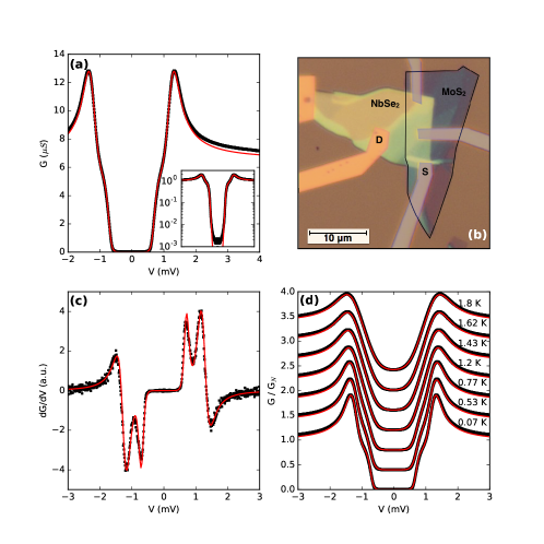
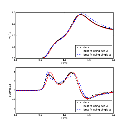
Fig. 1b shows a typical junction (‘Device A’) consisting of a 4-5 layer thick barrier (Supplementary Section 2) with a transparency (Supplementary Secion 6). Its normal state conductance 7S for an area 1.6 . Fig. 1a. shows the differential conductance as a function of (normalized to ) obtained with Device A, at . This spectrum has two striking features: First, the very low sub-gap conductance (), evident in the logarithmic plot presented at the inset. The residual conductance is likely due to environment-assisted tunneling (Supplementary Section 7). Second, the intricate structure of the quasiparticle peak. This spectrum differs from a standard BCS DOS by having a relatively low quasiparticle peak and a shoulder at lower energies. The latter feature can be clearly seen in the second derivative (Fig. 1c) where the slope separates into a double peak feature. In what follows, we begin by analyzing the structure of the quasiparticle peak using the two-band model. We then present measurements in magnetic field, where the low sub-gap background allows us to observe vortex bound states.
Two-band superconductivity was first discussed theoretically by Suhl et al. Suhl1959 , who considered distinct BCS coupling strengths for each band and allowed for Cooper-pair tunneling between bands. Schopohl and Scharnberg expanded on this, including inter-band single-electron scattering (parametrised by ), in addition to Cooper pair tunneling Schopohi1977a . These interband processes give rise to modified pairing amplitudes , resulting in a model corresponding to McMillan’s description of the proximity effect between a superconductor and a normal metal McMillan1968 . The resulting “SSM” model has successfully been used to fit tunneling conductance data from SIS junctions Schmidt , as well as scanning tunneling spectroscopy data from , indicating the two-band nature of these materials.
In the SSM model, the superconducting gaps in the two bands are found by solving the coupled equations
| (1) |
whereas the DOS of each band is given by
| (2) |
Here is the DOS at the Fermi energy in the normal state in band . The conductance is calculated by convolution of the DOS with the derivative of a Fermi-Dirac distribution with temperature , accounting for a ratio between the tunneling matrix elements for the two bands,
The best fit to our data with the above equations is shown in Fig. 1a, where the following fitting parameters are extracted : , , , , , and . As seen in the figure, our fit is remarkably precise - successfully reproducing both the first and second derivative experimental curves. It allows us to confirm the SSM model and determine the various parameters with unprecedented fidelity. The most salient feature in our fit is the identification of intrinsic superconducting pairing in the second band, manifest as . This yields a better fit to the data (Supplementary Fig. 3) than the alternative (), which corresponds to induced pairing Noat2015 . These same parameters yield successful fits also at elevated temperatures, while changing only (panel (d)). At the lowest temperature, however, the fitting temperature exceeds the expected electron temperature. It is unlikely that this is due to junction heating, and we suggest it is associated with inhomogeneity in (Supplementary Section 8).
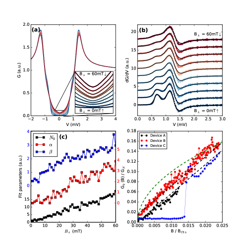
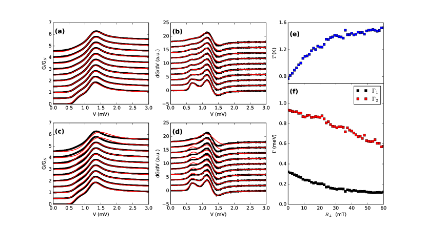
We now turn to the response of the tunneling spectrum to perpendicular magnetic field , shown in Fig. 2. Panel (a) shows a collection of curves taken at perpendicular magnetic fields mT. The data show that has two observable consequences: (i) it suppresses the lower energy shoulder of the quasiparticle peaks, seen most clearly in the plots in panel (b), and (ii) it increases the subgap signal (for ), seen in the inset. We find that in this low magnetic field it is possible to fit the modified spectra using the same 2-band model as the zero field data. The fit is superimposed on the data in panel (b), and details of the fitting parameters are discussed in Supplementary Section 5.
In type-II superconductors above vortices penetrate the sample. In this so-called “mixed state” the superconductor consists of quasi-normal vortex cores, and a gapped inter-vortex area. Due to the hard gap, our measurement spectrally differentiates between these regions: at low bias, sub-gap tunneling takes place only near the vortex cores. At higher bias, quasiparticle tunneling occurs at the entire area of the sample. In the remainder of this letter we provide further evidence that the sub-gap signal is associated with vortex-bound states.
Close inspection of the low bias region in Fig. 2a (inset) shows the onset of V-shaped spectra at low magnetic fields. As shown by Nakai et al. Nakai2006a such spectra are inherent to the integrated spectral weight of vortex-bound states, regardless of the symmetry of the order parameter. These comprise of zero-bias spectral weight and annular states centered at an energy-linear radius. Upon polar integration, the latter yield the term .
Finally, ref. Nakai2006a also identifies a quadratic term, . We carry out the same fit: , and extract the dependence of , and on . The -dependent fitting parameters are shown in Fig. 2c, where it is evident that all three increase monotonously with . We interpret as the product of the zero-energy DOS at each vortex, times the number of vortices accessible to the tunnel junction. For -wave superconductors is linear in field Nakai2004b , and can gauge the number of vortices in the junction. The dependence of , which also exhibits a linear increase with , can be interpreted in a similar way, since it represents a population of off-center states which are associated with individual vortices. The interpretation of is somewhat less straightforward. We will argue below that it is associated with currents induced around the vortices. We conclude that the subgap signal, and especially the linear term in the signal, is a good proxy for probing vortex penetration of the sample.
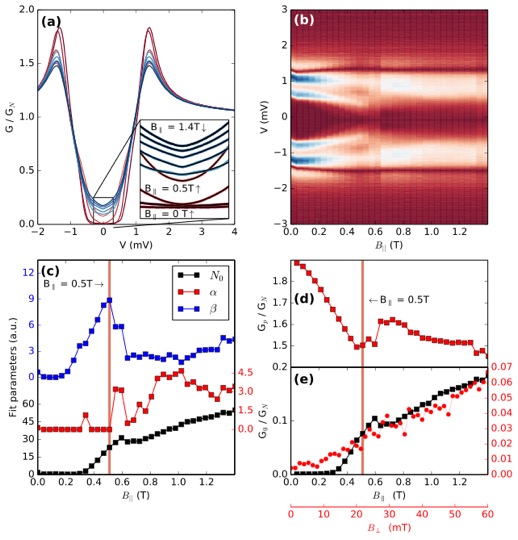
We repeat the same measurement and analysis for magnetic field applied parallel to the sample, (Fig. 3), up to 1.5T. Once again, we can follow the evolution of the low energy shoulder, which appears as a peak in (panel b). Here, unlike the case, this feature remains resolved as increases, but shifts to lower energies. We attribute this to Abrikosov-Gor’kov depairing AbrikosovA.A.1961ContributionImpurities ; Maki1964TheCurrents ; Levine1967DensityTunneling ; Millstein1967TunnelingField ; Anthore2003 , though here the effect is somewhat more complex than what was seen in previous works due to the 2-band nature of Kaiser1970McMillanAlloys .
The signal changes abruptly at , which we associate with . It is manifest as an increase of the height of the quasiparticle peak (panel d) and a sharp increase of the zero bias signal (panels c,e). We rule out the possible contribution of residual perpendicular fields, due to misalignment of the sample with the parallel field; this is compensated to better than 0.5% of the parallel field. Tunneling investigation away from perpendicular fields was carried out by Hess et al. Hess1994 , who observed complex flux lattices at various angles, and strictly parallel flux lines were observed in ref. Fridman2011a , where the Meissner currents indicated the positions of buried vortices. However, all these studies utilized bulk samples, whereas our sample thickness is , imposing spacial restrictions on the Meissner currents.
To probe the nature of this regime, we apply the same sub-gap analysis carried out for (Inset to Fig. 3a). For , the signal is described by a parabola with zero-offest, such that both and remain small, while increases. For , we find that drops sharply. This is accompanied by an increase in and , consistent with the onset of vortex tunneling. The drop in suggests that the parabolic term is partly a consequence of the Meissner currents, which drop sharply above . The appearance of vortex-bound and terms suggests that vortex sub-gap tunneling is taking place, similar to the case. This in turn, indicates tunneling accessibility to points where flux lines enter and exit the sample, likely due to defects or variations in thickness. In the alternative scenario, where flux lines are strictly parallel and are buried under the surface Fridman2011a , vortex-bound states would not be observable.
We now turn to discussion of the zero-bias conductance, and its dependence on . For (Fig. 2d), it is likely that the onset of vortex penetration is very close to . increases linearly with , consistent with a constant increase of vortex population. Following ref. Nakai2004b , we present vs. (dimensionless units). The data of Device A (black dots), follow a slope , reflecting a rapid increase in bound-state spectral weight. This slope appears to be generic, as two other devices (B and C, red and blue dots) exhibit a similar slope, noting that in Device C there is a finite onset field. For -wave superconductors one expects minimal vortex overlap, resulting in a minimal slope of 1.2 Nakai2004b , where exceeding this value could indicate deviations from perfect isotropy. These, however, would modify the quasi-particle peak structure. Based on the broadening we actually observe, the anisotropy remains capped by 1.2 (Supplementary Section 8), and hence cannot be the origin of the high spectral weight we observe. It is also not compatible with line-node anisotropy since the zero bias signal clearly deviates from a square root dependence expected in this case. A possible explanation is a renormalisation of the local magnetic field at the junction due to flux focusing.
Our work opens up the possibility of using vdW barriers to investigate the density of states of other vdW materials, and in particular superconductors Lu_MoS2_2015 ; Saito_MoS2_2015 ; Xi_2016 . As vdW tunnel barriers adhere readily to clean, flat surfaces, they could also be deposited on non-vdW (super)conductors. Furthermore, as the dry transfer technique does not involve solvents, and as the resulting device size is compatible with custom mechanical masks (thus eliminating the need for lithography), vdW tunnel barriers could perhaps also be deposited on organic (super)conductors and other fragile systems which have hitherto not been investigated in tunnel spectroscopy. Finally, we note that fabricating multiple, closely-spaced tunnel electrodes on the same device — a feasible extension of our present methods — will allow the investigation of many new systems under non-equilibrium conditions Clarke ; Gray ; Jedema ; Quay ; Hubler
Methods
The vdW tunnel junctions were fabricated using the dry transfer technique Castellanos-Gomez2014 , carried out in a glove-box (nitrogen atmosphere). flakes were cleaved using the scotch tape method, peeled on commercially available Gelfilm from Gelpack, and subsequently transferred to a substrate. and flakes were peeled in a same way, where thin flakes suitable for the formation of tunnel barriers were selected based on optical transparency. The barrier flake was then transferred and positioned on top of the flake at room temperature. Ti/Au contacts and tunnel electrodes were fabricated using standard e-beam techniques. Prior to the evaporation of the ohmic contacts the sample was ion milled for 15 seconds. No such treatment was done with the evaporation of the tunnel electrodes. All transport measurements were done in a 3He–4He dilution refrigerator with a base temperature of 70 mK. The AC excitation voltage was modulated at 17 Hz; its amplitude was 15V at all temperatures. Measurement circuit details are provided in Supplementary Section 1.
Acknowledgements
We thank P. Février and J. Gabelli for helpful discussions on tunnel barriers, and T. Cren for the same on . This work was funded by a Maimonïdes-Israel grant from the Israeli-French High Council for Scientific & Technological Research; ERC-2014-STG Grant No. 637298. (TUNNEL); and an ANR JCJC grant (SPINOES) from the French Agence Nationale de Recherche. T.D. is grateful to the Azrieli Foundation for an Azrieli Fellowship. L.A. and M.K. are supported by the Israeli Science Foundation, Grant No. 1287/15.
Author contributions
T.D. fabricated the devices. T.D. and C.Q.H.L. performed the measurements. All the authors contributed to data analysis and the writing of the manuscript.
Competing financial interests
The authors declare no competing financial interests.
References
- (1) Giaever, I. Energy gap in superconductors measured by electron tunneling. Physical Review Letters 5, 147–148 (1960).
- (2) McMillan, W. L. Tunneling model of the superconducting proximity effect. Physical Review 175, 537–542 (1968).
- (3) Rowell, J. M. Tunneling observation of bound states in a normal metal-superconductor sandwich. Physical Review Letters 30, 167–170 (1973).
- (4) Dynes, R. C., Narayanamurti, V. & Garno, J. P. Direct measurement of quasiparticle-lifetime broadening in a strong-coupled superconductor. Physical Review Letters (1978).
- (5) Dynes, R. C., Garno, J. P., Hertel, G. B. & Orlando, T. P. Tunneling Study of Superconductivity near the Metal-Insulator Transition. Physical Review Letters 53, 2437–2440 (1984).
- (6) Fert, A. Origin, development, and future of spintronics (Nobel lecture). Review of Modern Physics 80, 1517–1530 (2008).
- (7) Kastner, M. A. The single-electron transistor. Reviews of Modern Physics 64, 849 (1992).
- (8) Wolf, E. L. Principles of Electron Tunneling Spectroscopy (OUP, Oxford, 2011), 2 edn.
- (9) Giazotto, F., Heikkilä, T. T., Luukanen, A., Savin, A. M. & Pekola, J. P. Opportunities for mesoscopics in thermometry and refrigeration: Physics and applications. Rev. Mod. Phys. 78, 217–274 (2006).
- (10) van der Wal, C. H. et al. Quantum Superposition of Macroscopic Persistent-Current States. Science 290, 773–777 (2000).
- (11) Devoret, M. H. & Schoelkopf, R. J. Superconducting Circuits for Quantum Information: An Outlook. Science 339, 1169–1174 (2013).
- (12) Geim, A. K. & Grigorieva, I. V. Van der Waals heterostructures. Nature 499, 419–425 (2013).
- (13) Dean, C. R. et al. Boron nitride substrates for high-quality graphene electronics. Nature nanotechnology 5, 722–726 (2010).
- (14) Amet, F. et al. Tunneling spectroscopy of graphene-boron-nitride heterostructures. Physical Review B 85 (2012).
- (15) Britnell, L. et al. Electron tunneling through ultrathin boron nitride crystalline barriers. Nano Letters 12, 1707–1710 (2012).
- (16) Chandni, U., Watanabe, K., Taniguchi, T. & Eisenstein, J. P. Signatures of phonon and defect-assisted tunneling in planar metal-hexagonal boron nitride-graphene junctions. Nano letters 16, 7982–7987 (2016).
- (17) Schopohl, N. & Scharnberg, K. Tunneling Density of States for the Two-Band Model of Superconductivity. Solid State Communications 22, 37–1 (1977).
- (18) Noat, Y. et al. Quasiparticle spectra of 2H-NbSe2: Two-band superconductivity and the role of tunneling selectivity. Physical Review B 92, 1–18 (2015).
- (19) Nakai, N., Miranović, P., Ichioka, M. & Machida, K. Field dependence of the zero-energy density of states around vortices in an anisotropic-gap superconductor. Physical Review B 70 (2004).
- (20) Nakai, N. et al. Ubiquitous V-shape density of states in a mixed state of clean limit type II superconductors. Physical Review Letters 97, 2–5 (2006).
- (21) Clarke, J. Experimental observation of Pair-Quasiparticle potential difference in Nonequilibrium superconducors. Phys. Rev. Lett. (1972).
- (22) Jedema, F. J., Filip, A. T. & van Wees, B. J. Electrical spin injection and accumulation at room temperature in an all-metal mesoscopic spin valve. Nature 410, 345–348 (2001).
- (23) Quay, C. H. L., Chevallier, D., Bena, C. & Aprili, M. Spin imbalance and spin-charge separation in a mesoscopic superconductor. Nature Physics 9, 84–88 (2013).
- (24) Hübler, F., Wolf, M. J., Beckmann, D. & V. L??hneysen, H. Long-range spin-polarized quasiparticle transport in mesoscopic al superconductors with a zeeman splitting. Physical Review Letters (2012).
- (25) Caroli, C., De Gennes, P. & Matricon, J. Bound Fermion states on a vortex line in a type II superconductor. Physics Letters 9, 307–309 (1964).
- (26) Andreev, A. F. The Thermal Conductivity of the Intermediate State in Superconductors. J. Exptl. Theoret. Phys. (U.S.S.R.) 19, 1823–1828 (1964).
- (27) de Gennes, P. G. & Saint-James, D. Elementary Excitations in the Vicinity of a Normal Metal-Superconducting Metal Contact. Physics Letters 4, 151 (1963).
- (28) Pillet, J.-D. et al. Andreev bound states in supercurrent-carrying carbon nanotubes revealed. Nature Physics 6, 965 (2010).
- (29) Dirks, T. et al. Transport through Andreev bound states in a graphene quantum dot. Nature Physics 7 (2011).
- (30) Kane, C. L. & Fu, L. Superconducting Proximity Effect and Majorana Fermions at the Surface. Physical Review Letters 096407 (2008).
- (31) Kopnin, N. B. & Sonin, E. B. BCS Superconductivity of Dirac electrons in graphene layers. Physical review letters 100, 246808 (2008).
- (32) Khaymovich, I. M., Kopnin, N. B., Mel’Nikov, A. S. & Shereshevskii, I. A. Vortex core states in superconducting graphene. Physical Review B - Condensed Matter and Materials Physics 79 (2009).
- (33) Das, A. et al. Zero-bias peaks and splitting in an Al-InAs nanowire topological superconductor as a signature of Majorana fermions. Nature Physics 8, 887–895 (2012).
- (34) Mourik, V. et al. Signatures of Majorana Fermions in Hybrid Superconductor-Semiconductor Nanowire Devices, vol. 336 (2012).
- (35) Schrieffer, J. Theory of superconductivity (W.A. Benjamin, Inc.,New York, 1964).
- (36) Blonder, G. E., Tinkham, M. & Klapwijk, T. M. Transition from metallic to tunneling regimes in superconducting microconstrictions: Excess current, charge imbalance, and supercurrent conversion. Physical Review B 25, 4515–4532 (1982).
- (37) Kleinsasser, A. W., Rammo, F. M., Bhushan, M., Rammoa, F. M. & Bhushanb, M. Degradation of superconducting tunnel junction characteristics with increasing barrier transparency. Applied Physics Letters 62, 1017–212504 (1993).
- (38) Greibe, T. et al. Are "pinholes" the cause of excess current in superconducting tunnel junctions? A study of Andreev current in highly resistive junctions. Physical Review Letters 106 (2011).
- (39) Pekola, J. P. et al. Environment-Assisted Tunneling as an Origin of the Dynes Density of States. Physical Review Letters 105, 026803 (2010).
- (40) Di Marco, A., Maisi, V. F., Pekola, J. P. & Hekking, F. W. J. Leakage current of a superconductor-normal metal tunnel junction connected to a high-temperature environment. Physical Review B - Condensed Matter and Materials Physics 88 (2013).
- (41) Chang, W. et al. Hard gap in epitaxial semiconductor-superconductor nanowires. Nature nanotechnology 10, 232–6 (2015).
- (42) Suhl, H., Matthias, B. T. & Walker, L. R. Bardeen-Cooper-Schrieffer Theory of superconductivity in the case of overlapping bands. Physical Review Letters 3, 552–554 (1959).
- (43) Schmidt, H., Zasadzinski, J. F., Gray, K. E. & Hinks, D. G. Break-junction tunneling on MgB2. Physica C: Superconductivity and its Applications 385, 221–232 (2003).
- (44) Abrikosov A.A. & Gor’kov L.P. Contribution to the Theory of Superconducting Alloys with Paramagnetic Impurities. Soviet Physics JETP 12, 1243 (1961).
- (45) Maki, K. The Behavior of Superconducting Thin Films in the Presence of Magnetic Fields and Currents. Progress of Theoretical Physics 31, 731–741 (1964).
- (46) Levine, J. L. Density of States of a Short-Mean-Free-Path Superconductor in a Magnetic Field by Electron Tunneling. Physical Review 155, 373 (1967).
- (47) Millstein, J. & Tinkham, M. Tunneling into superconducting films in a magnetic field. Physical Review 158, 325–332 (1967).
- (48) Anthore, A., Pothier, H. & Esteve, D. Density of states in a superconductor carrying a supercurrent. Physical review letters 90, 127001 (2003).
- (49) Kaiser, A. B. & Zuckermann, M. J. McMillan model of the superconducting proximity effect for dilute magnetic alloys. Physical Review B 1, 229–235 (1970).
- (50) Hess, H. F., Murray, C. A. & Waszczak, J. V. Flux lattice and vortex structure in 2H-NbSe2 in inclined fields. Physical Review B 50, 16528–16540 (1994).
- (51) Fridman, I., Kloc, C., Petrovic, C. & Wei, J. Y. T. Lateral imaging of the superconducting vortex lattice using Doppler-modulated scanning tunneling microscopy. Applied Physics Letters 99 (2011).
- (52) Lu, J. M. et al. Evidence for two-dimensional Ising superconductivity in gated MoS2. Science 350, 1353–1357 (2015).
- (53) Saito, Y. et al. Superconductivity protected by spin–valley locking in ion-gated MoS2. Nature Physics 12, 144–149 (2015).
- (54) Xi, X. et al. Ising pairing in superconducting NbSe2 atomic layers. Nature Physics 12, 139–143 (2016).
- (55) Gray (Ed.), K. E. Nonequilibrium Superconductivity, Phonons, and Kapitza Boundaries (Spinger, Berlin, 1981).
- (56) Castellanos-Gomez, A. et al. Deterministic transfer of two-dimensional materials by all-dry viscoelastic stamping. 2D Materials 1, 011002 (2014).
- (57) Anderson, P. Theory of dirty superconductors. Journal of Physics and Chemistry of Solids 11, 26–30 (1959).
- (58) Gygi, F. & Schlüter, M. Self-consistent electronic structure of a vortex line in a type-II superconductor. Physical Review B 43, 7609–7621 (1991).
- (59) Sharvin, Y. V. A possible method for studying Fermi surfaces. JETP 48, 984–985 (1965).
- (60) Griffiths, D. J. Introduction to quantum mechanics (Pearson Education India, 2005).
- (61) Brinkman, W. F., Dynes, R. C. & Rowell, J. M. Tunneling Conductance of Asymmetrical Barriers. Journal of Applied Physics 41, 1915 (1970).
- (62) Di Marco, A., Maisi, V. F., Pekola, J. P. & Hekking, F. W. J. Leakage current of a superconductor-normal metal tunnel junction connected to a high-temperature environment. Physical Review B - Condensed Matter and Materials Physics 88 (2013).
Supplemental Materials: Hard superconducting gap and vortex-state spectroscopy in NbSe2 van der Waals tunnel junctions
S1 Details of the measurement setup
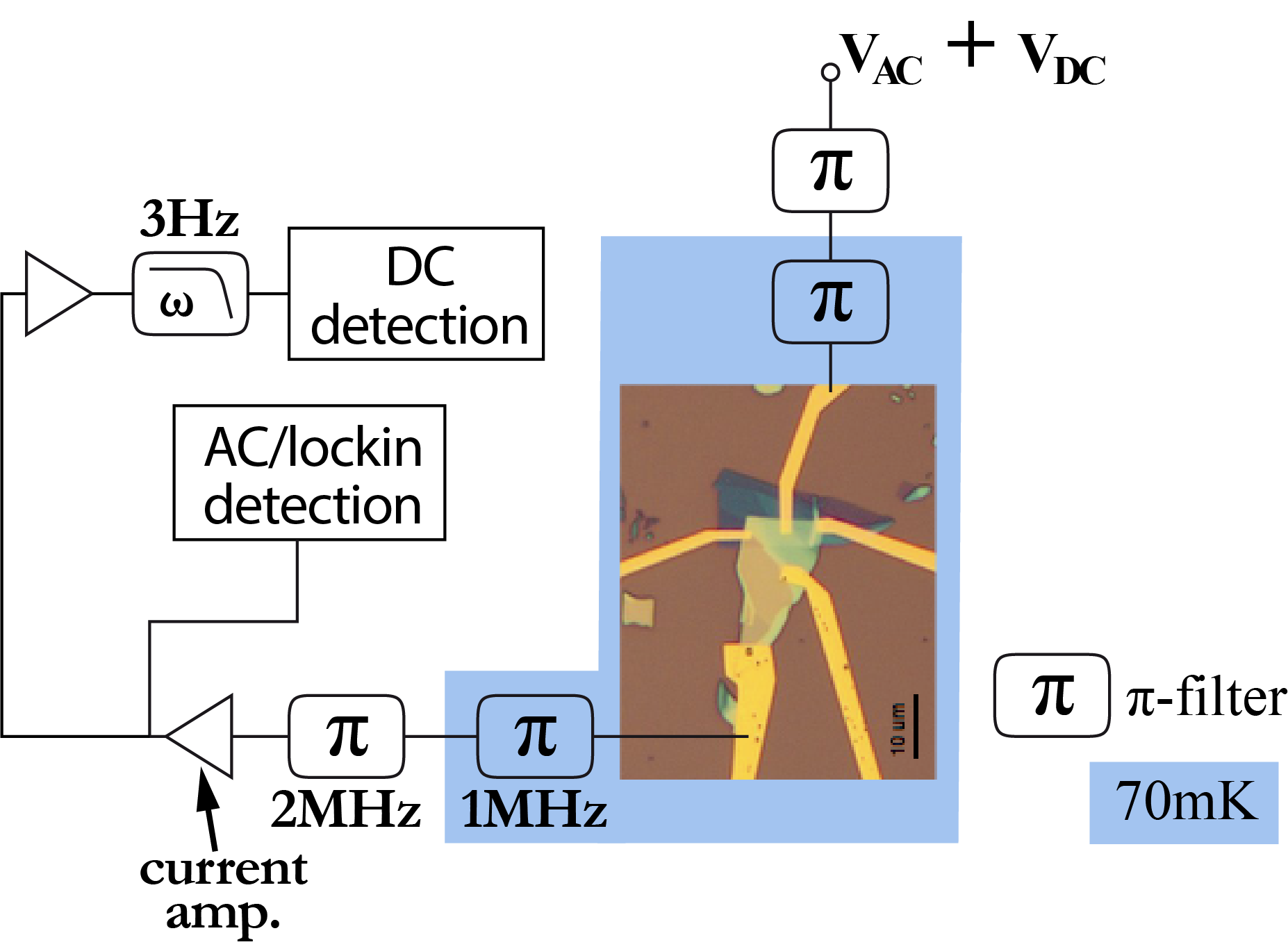
Figure S1 shows our measurement circuit in greater detail than was presented in the main text. All -filters at low temperature have cutoff frequencies of 1MHz while those at room temperature have cutoff frequencies of 2MHz. The amplitude of the AC excitation is 15V in all the figures of the main text. Measurements at lower showed that, between 2V and 15V, there was no discernible distortion of ; the higher excitation voltage was thus chosen in order to have a better signal-to-noise ratio.
S2 Thickness and structure of the tunnel barrier
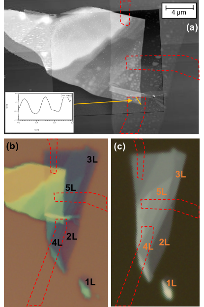
The high optical contrast between layers of different thickness of transition metal dichalcogenides (TMDs) allows easy identification of the thickness of the tunnel barrier. Figure S2 shows the optical image of the barrier on the PDMS immediately after it was exfoliated (panel c) and on top of the flake after the transfer procedure (panel b). Both show clearly that the source electrode was deposited above a region consisting of 4 and 5 layer thick . As a result of exponential dependence of the tunnel current on the barrier thickness, only the 4 layer part of the junction is significant to the measurement. Hence we expect the effective junction area to be 1.6 and the barrier thickness to be between 2.4 nm and 2.6 nm.
Contrary to the optical images, AFM does not provide a reliable measure of height between two different materials and cannot measure the thickness of the barrier. However AFM reveals some structures which are probably due to PDMS residue from the transfer process (panel a). A cross section of some of these features in the area of the junction shows height variation on the scale of 7 nm. The usual cleaning techniques of heat annealing cannot be used here due to the sensitivity of to heat. The effect of this structure is most likely to reduce the effective area of the junction to the non-contaminated region. As discussed in the next section, the effective area of the junction is of the same order of magnitude as the observed area, showing the robustness of this method to imperfections.
S3 Detailed derivation of the 2-band model
The model used to fit the data measured in this work, utilizes the McMillan equations McMillan1968 similar to the method presented in refs. Schmidt ; Noat2015 . These equations include the pairing amplitudes as fitting parameters. The pairing amplitudes, however, are not fundamental properties - they depend on the BCS coupling within the bands, between the bands, on the interband single electron scattering rates, and on the temperature. are therefore extracted from the fit of Eq. 1 in the main text, but can be calculated from fundamental properties. In this section we outline this calculation, using a model that fully includes all possible effects of two band superconductivity. We then check for consistency between the fit and the calculation.
The model Hamiltonian reads,
| (S1) |
where the terms, , and describe the band dispersion, Cooper channel interaction and disorder scattering respectively. We have
| (S2) | ||||
| (S3) | ||||
| (S4) | ||||
Here and are the creation operators of the electrons in Bloch states with momentum and spin in and bands respectively. In what follows, the index labels the bands. In the Hamiltonian, Eq. (S2), are the electron dispersion in band . The constants are Cooper channel interactions, and are inter- and intra-band disorder scattering potentials between momenta and . The dimensionless couplings are introduced as
| (S5) |
where is the normal state density of states in the band . Our sign convention in Eq. (S5) is such that positive couplings describe attraction. The first two terms of describe intra-band Cooper pair scattering and the latter two terms describe inter-band scattering. Notice that the intra-band single-electron disorder scattering in does not affect our results due to the Anderson theorem Anderson1959 , it is introduced here for completeness.
We then derive the self consistent equations in Matsubara formalism:
| (S6) | ||||
where,
| (S7) | ||||
and
| (S8) | ||||
We emphasize that this derivation is different from the McMillan derivation by the inclusion of the term i.e. Cooper pair tunneling between the bands. This term is irrelevant for the calculation of the proximity effect, but in principle should be present when discussing two band superconductivity.
We estimate by using the following values: = 1.1, = 0.38 meV (obtained from the fit), and = 0.22, = 0.13, = 0.001, and = 500 meV. Such a high value for is not physical. A more realistic value would be = 60 meV, and = 0.15, = 0.01, = 0.001. This results in = 1.15 meV, = 0.36 meV. The observed values of are on the high side for weak coupling given , suggesting that the weak-coupling assumption is only marginally valid.
S4 Intrinsic vs. induced 2nd order parameter
Although Noat et al. Noat2015 report a fit to a single intrinsic pairing amplitude while leaving the other one as induced, the SSM model can intrinsically support two pairing amplitudes. To distinguish between these two scenarios, we fit the measured curves in two different modes: (i) without any constraints, thus allowing both pairing amplitudes as fit parameters, and (ii) while fixing . The fits obtained are presented in figure S3 superimposed on the measured data. While both fits agree reasonably well with the curve (panel a), it is clear that the 2-order-parameter model fits the data better. This is seen more clearly in the second derivative. Here, the 2-order-parameter model traces the outer peak, while both models fall short of a perfect fit at the inner peak.
S5 2-band fit of tunneling data in magnetic field
We fit the curves measured with small perpendicular magnetic field using the zero field SSM model (figure S4). We begin with testing the more predictable model, where we assume the smaller gap is more fragile to magnetic fields. This model should yield lower while keeping the coupling parameters fixed. This, however, clearly fails to fit the data (panels c,d). The fit which does successfully reproduce the experimental curve (panels a,b), involves decreasing the inter-band coupling parameters, and (panel (f)). As these are associated with microscopic scattering processes, we don’t expect them to be sensitive to magnetic field, and hence the origin of their suppression remains unclear. The fit also yields an increase in effective temperature (panel (e)). Such temperature broadening of the coherence peaks could be a manifestation of spatially-dependent Abrikosov-Gor’kov (AG) corrections due to the currents around the vortices AbrikosovA.A.1961ContributionImpurities ; Maki1964TheCurrents . Quantitative modeling of this effect requires a detailed calculation incorporating the AG corrections into the McMillan model Kaiser1970McMillanAlloys , and calculating the spatially-varying vortex DOS, as has been done (without AG corrections) in Ref. Gygi1991Self-consistentSuperconductor for a single superconducting band.
S6 Estimate of the barrier transparency
We can estimate the transparency of our tunnel barrier from the well-known expression from Sharvin Sharvin1965 :
| (S9) |
where is the junction conductance in the normal state, is the area of the junction, the Fermi momentum and the average transmission of each conductance channel. We measure 7S for 1.6 . in metals is usually and it is about half this value in . Taking the lower value, we get .
We can make an independent estimate of using the textbook WKB formula for a square barrier of thickness and height Griffiths2005 :
| (S10) |
where is the effective mass of the electron in the barrier, here .
The gap of few layer at the point in the Brilloiun zone is on the order of 2eV, whereas the effective mass is generally a fraction of 1. Taking 1eV, ( being the bare electron mass), and in the range 2.4–2.6nm we find –, consistent with the Sharvin estimate.
We can make a more rigorous estimate of (and thus ) by using Brinkman et al.’s result Brinkman1970TunnelingBarriers for the conductance across a trapezoidal barrier with diffuse boundaries, together with measurements of the high bias conductance of our junction:
| (S11) |
where is the voltage across the barrier, is the mean barrier height, the barrier height difference on the two sides of the trapezoid, the barrier width and . In these expressions, is in units of Å, while , and are in units of volts.
Far from the Fermi level, the conductance of our junction indeed rises (Figure S5). This rise is not perfectly parabolic and is likely due, in part, to factors other than barrier transparency and asymmetry. Therefore, fitting a parabola to the background, i.e. assuming that the rise is due almost entirely to the barrier, will give us a worst case scenario or minimum possible barrier height.
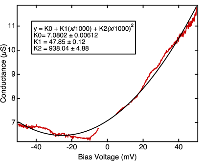
From the fit to our data to Equation S11 using = 20Å, we find 0.8V, not so different from what we assumed previously. If we use this, and 2.4–2.6nm as before, –.
Considering all of the above, is likely in the range or close to it.
S7 Possible origin of the sub-gap signal
At zero magnetic field, the sub-gap conductance of the measured tunnel junction at zero bias voltage is highly suppressed, to 1/500 of the normal state conductance. This residual conductance cannot be accounted for by the thermal broadening of the SSM model, as this gives negligible values at the sub-kelvin temperature range.
In principle, one or more of the following could be responsible for the sub gap signal: (i) pair tunnelling (due to Andreev reflection) Blonder1982 ; (ii) environment-assisted tunnelling, which can be described by a ‘Dynes’ parameter in the BCS density of states (an imaginary part in the energy)Pekola2010Environment-AssistedStates ; Marco2013 ; (iii) a finite quasiparticle lifetime, due e.g. to strong electron-phonon coupling, which is also described by a Dynes parameter Dynes1978 ; and (iv) a parallel resistance in the junction.
In Figure S6, we show the conductance of the junction at energies below the gap and compare it to two theoretical calculations. A fit to the data using the the SSM model with the inclusion of the Dynes terms produces the curve shown in green, which shows good agreement.
If, on the other hand, we assume that the conductance at is due entirely to Andreev processes, using the Blonder, Tinkham and Klapwijk (BTK) model Blonder1982 – using a single band BCS density of states with meV, the apparent size of the gap, and normalised to the measured – we obtain a curve which also fits the data in the low bias region. However, we find for the dimensionless barrier strength, which corresponds to a transparency , much greater than the value obtained in the previous section and thus not plausible.
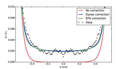
In addition, we note that in Al//Al NIS junctions (200nm 200nm, 5–10k) measured in the same dilution refrigerator with the same measurement setup, is typically 1/200. According to Ref. Pekola2010Environment-AssistedStates , for a given environment, the environmental contribution to the subgap conductance should be suppressed if either or , the capacitance of the junction, increases. As both of and of the device are higher than the Al device, we expect further suppression of , and this is indeed what we see.
All of the above would seem to suggest that the subgap conductance is not limited by Andreev processes but rather by the environment. We cannot, however, rule out the contribution of finite quasiparticle lifetimes or a resistance parallel to the junction.
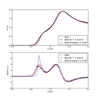
S8 Possible origin of the effective temperature
As mentioned in the main text and as can be seen in Figure S7 below, the curve of our device agrees very well with the SSM model, with an effective temperature of 500mK — significantly higher than the known base electron temperature of the dilution refrigerator used, which is 100mK. This could be due to some combination of: (i) heating from the measurement; (ii) a slight -space anisotropy in ; and (iii) defects in the such as Se vacancies leading to spatially inhomogeneous ’s and ’s. We explore each of these explanations in turn.
Equating the heat produced by the junction () with the heat carried away by the leads () and using the Wiedemann-Franz law (), we obtain
| (S12) |
Here is the current and the voltage across the junction. is the thermal conductivity, the thickness and the resistance of the leads; the number of squares in the leads and the temperature difference across the leads. is the Lorenz number.
As the discrepancy between the constrained and unconstrained fits in Figure S7 are most evident well below 1mV, we take = 1mV, = 3nA and . measured at 4K is 205 and can only decrease at the base temperature of the refrigerator. This yields , which is too small to explain the observed effective temperature.
It would therefore seem that gap anisotropy (in -space) or inhomogeneity (in real space) is responsible for the observed effective temperature.
If we assume that -space gap anisotropy is the only mechanism responsible for the effective temperature, we can put an upper bound on the gap anisotropy of in the plane, by assuming that the FWHM of the derivative of the Fermi-Dirac function.
| (S13) |
We note that this level of anisotropy is indistinguishable from perfect isotropy in its effect on the slope of the zero bias conductance as a function of field (cf. Fig. 2b of main text).
Finally, and more speculatively, we note that an effect such as a -space dependence of the inter-band couplings could also be responsible for .