High-sensitivity, spin-based electrometry with an
ensemble of nitrogen-vacancy centers in diamond
Abstract
We demonstrate a spin-based, all-dielectric electrometer based on an ensemble of nitrogen-vacancy (NV-) defects in diamond. An applied electric field causes energy level shifts symmetrically away from the NV-’s degenerate triplet states via the Stark effect; this symmetry provides immunity to temperature fluctuations allowing for shot-noise-limited detection. Using an ensemble of NV-s, we demonstrate shot-noise limited sensitivities approaching 1 V/cm/ under ambient conditions, at low frequencies (10 Hz), and over a large dynamic range (20 dB). A theoretical model for the ensemble of NV-s fits well with measurements of the ground-state electric susceptibility parameter, . Implications of spin-based, dielectric sensors for micron-scale electric-field sensing are discussed.
I Introduction
The detection of weak electric signals in low-frequency regimes is important for areas of research such as particle physics Sharma et al. (2016), atmospheric sciences Merceret et al. (2008); Simoes et al. (2012); Mezuman et al. (2014), and neuroscience Barry et al. (2016). Commonly available ambient electrometers that rely on electrostatic induction, like field mills Fort et al. (2011); Riehl et al. (2003) and dipole antennas Harrington (1960), are physically limited in size to several tens of centimeters by the wavelength of the electric field of interest. This hinders miniaturization at frequencies below several Hertz Chu (1948); Harrington (1960); Chubb (2015); Barr et al. (2000). Fully dielectric sensors allow sensing of electric fields without fundamental constraints on the size of the sensor and do not distort the incident field Savchenkov et al. (2014); Toney (2015). Ongoing efforts to develop compact electrometers include use of the electro-optic effect within solid-state crystals Vohra et al. (1991), single electron transistors Lee et al. (2008); Vincent et al. (2004); Neumann et al. (2013a), and the energy shifts induced by electric fields of atom-based sensors such as trapped ions Bruzewicz et al. (2015) or Rydberg atoms Osterwalder and Merkt (1999); Sedlacek et al. (2012). Recently, optically-addressable electron spins in solid-state materials have played a central role in the development of quantum sensing Awschalom et al. (2013); Degen et al. (2016). Compared with atom-based approaches that require vacuum systems, these systems allow for a higher density of spins with a reduced experimental footprint, along with other promising properties such as long room-temperature coherence times and optical accessibility for spin initialization and readout Acosta and Hemmer (2013).

Among spin-based sensors, there has been significant progress in using ensembles of spins in diamond for sensing magnetic fields Clevenson et al. (2015); Fang et al. (2013); Barry et al. (2016), while work in diamond-based electrometry has primarily focused on the use of single spins Dolde et al. (2011); Doherty et al. (2014). Here, we experimentally demonstrate a spin-based, solid-state electrometer that is sensitive to the electric field induced Stark shift on an ensemble of negatively-charged nitrogen-vacancy (NV-) color centers while being robust, to first order, to temperature fluctuations. Our diamond-based electrometer operates at shot-noise limited sensitivities of under ambient conditions at extremely low frequencies (0.05-10 Hz) without repetitive readout and dynamic decoupling control necessary for electrometry with single NV-s Dolde et al. (2011). By utilizing a high degree of symmetry to overcome the inhomogeneous strain and non-collinear crystallographic orientations within an ensemble of NV-s, this work brings diamond-based electrometry into a regime where it has a competitive sensitivity with a clear path towards miniaturization.
NV- centers are sensitive to electric fields in both their optical ground Dolde et al. (2011) and excited triplet states Tamarat et al. (2006). Previously, electric field sensing with a single NV- was demonstrated with sensitivity down to 202 V/cm/ (891 ) at a frequency of kHz (DC) under precisely applied magnetic fields, but the need for repetitive readout and dynamic decoupling pulse control limited that technique to frequencies in excess of 10 kHz due to the NV-’s decoherence rate (1/T2 where T ms). The device demonstrated here uses an ensemble of NV- centers in an otherwise similarly sized diamond. It is not only possible to achieve higher sensitivities (albeit over a larger volume), but it also allows for a measurement of the noise spectral density (NSD) due to low-frequency electric field fluctuations irrespective of temperature fluctuations. Furthermore, the introduced method allows for highly accurate measurement of the transverse electric susceptibility parameter, , of the NV-’s ground state. By using this measurement modality, we expect that a diamond that is densely populated with NV-s would yield a projected shot-noise-limited electric field sensitivity approaching 111See Supplemental Material at [URL will be inserted by publisher] for this projected sensitivity using values from recent magnetometry experiments Barry et al. (2016)., making NV--based electrometers comparable with currently existing, room-temperature, solid-state electrometers Savchenkov et al. (2014); Toney (2015).
II Theory of NV- electrometry
The physical mechanism of the NV-’s sensitivity to electric fields originates from its optical excited state configuration, which is a highly electric field sensitive molecular doublet (). Stark shifts of the excited state cannot be measured optically under ambient conditions due to phonon-induced mixing Plakhotnik et al. (2014). However within each orbital of the molecular doublet, the electric field induced splitting of the hyperfine manifold can be detected by optically detectable magnetic resonance (ODMR). Additionally, the excited-state orbital overlaps sufficiently with the ground-state molecular orbital () to also impart electric field sensitivity on the ground state spin configuration of the NV- Doherty et al. (2014).
The Hamiltonian describing both the triplet ground and excited states of the NV- share the following form Doherty et al. (2013):
| (1) |
where is the crystal field splitting (Hz), is the gyromagnetic ratio (), is the axial electric field dipole moment (), is the axial electric field (V/cm), is the magnetic field vector, is the g-factor tensor, is the vector of electronic spin-1 Pauli operators, is the hyperfine tensor, and is the vector of nuclear spin-1 Pauli operators. Because an electric field’s effect on the NV- spin is significantly smaller than the crystal field splitting (), the transverse electric field dependence can be considered as a perturbation to the Hamiltonian:
| (2) |
where is the ground-state’s transverse electric field dipole moment 222See Doherty et al. (2014) for the relationship between electric-dipole moment, and the electric susceptibility, ., and are the cartesian components of the combined strain and electric fields 333See Fig. 7 for the differences and similarities in using the ground and excited states of the NV-for electrometry, and (for ) are the spin-1 Pauli operators of the electronic spin. After diagonalizing Eqn. (1) and using Eqn. (2) as the perturbation, there is a closed-form equation which describes the effect of electric and magnetic fields on the NV- (See Eqn. S1). The following equation accurately describes how the eigenfrequencies of a single NV-change under an applied electric field () alongside no magnetic field (). Furthermore, the expression quantitatively matches the transition shifts due to a symmetric application of electric fields on all eight classes of defects within an ensemble of NV- centers:
| (3) |
where is the crystal field splitting with a temperature dependence of 77 kHz/Kelvin Chen et al. (2011), and are the electric susceptibility parameters (in units of ), and and are the electric field amplitudes (in units of V/cm) parallel and perpendicular, respectively, to the NV- symmetry axis.
The shot-noise sensitivity to the transverse electric field (in ) limits using an ensemble of NV-s is given by the following:
| (4) |
where is the contrast of the ensemble ODMR spectra, is the total photon collection rate per NV-, and is the inhomogeneous NV- coherence time. Using our experimentally measured values, we arrive at a shot-noise limit approaching for the NV- ground state 444 . This expression shows that the sensitivity limit depends on the density of NV-s in the sample, the coherence properties of the NV-s, and the efficiency of photon collection.
III Experimental Results
The diamond measured in this work is 3.0 x 3.0 x 0.32 in size and contains an NV- density of 1 ppb produced during the chemical vapor growth process. The two square faces on which the electrodes were evaporated have crystallographic orientations (See Fig. 1), and thus the applied electric field produces an equal projection onto all eight orientations of NVs within the ensemble. We measured ODMR of the ensemble of NV-s using continuous-wave (CW) laser and microwave excitation from the side and bottom, respectively.
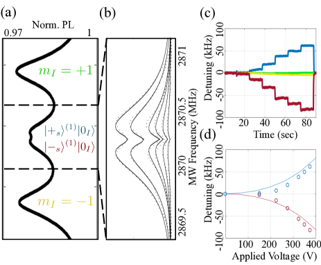
To account for the distribution of strain magnitudes and angles within the ensemble of NV-s, we use the (2,1) Gamma probability distribution as an ansatz for the magnitude distribution, and assume a uniform and isotropic angular distribution 555See Supplemental Material at [URL will be inserted by publisher] for an analysis considering the isotropic distribution of strain with an ensemble of NV-s.. This model accounting for the isotropic distribution of strain accurately fits the experimental data (See Fig. 2b). We also simulated the expected electric field induced shift on the ensemble average of NV-s in Fig. 2c using an estimated distribution of strain. The simulated results match well with the step-wise increase in electric field; this agreement validated the use of this method for accurately scaling the measured shift in frequency to the reported noise floor of the noise spectral density (See Figures 2c,d).
To detect a shift in NV- transition frequencies of the NV-ensemble due to an external electric field, the magnetic field along the NV- axes must be significantly weaker than the internal electric or strain fields. The maximum electric field sensitivity is achieved at zero magnetic field, but at the expense of vector sensitivity Dolde et al. (2011). Additionally, the shot-noise limited sensitivity given by Eqn. 4 can be optimized by controlling the laser and microwave excitation powers.
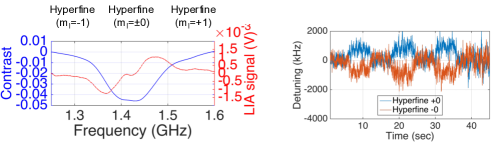
We measured two electric and strain sensitive transition frequencies (denoted as ) simultaneously at a rate inversely proportional to the time constant of the home-built lock-in instrumentation 666See Supplemental Material at [URL will be inserted by publisher] for a description of the technical details of the setup.. Although only the two transitions are monitored, the shift in frequencies correspond to an average shift due to the entire ensemble. The inhomogeneous strain typically found in the ensemble is indistinguishable from an inhomogeneous distribution of electric fields. Using a bias electric field beyond the average strain of the ensemble of NV- centers, the shift of the (See Fig. 1 for notation) transitions become linearly sensitive to electric fields, while the transitions, , remain relatively insensitive to electric fields due to the quadrupole field of the host nuclear spin (See Fig.2d).
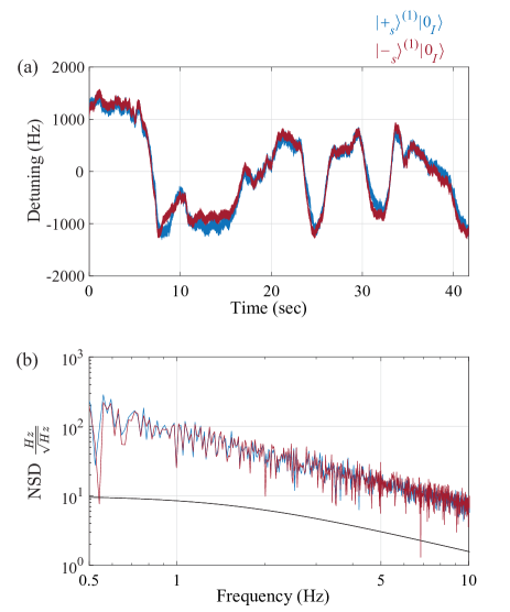
Figure 3 presents the resulting sensitivity measurements. A maximum electric field sensitivity of the ensemble of NV-s was achieved with an incident laser power of 1.8 W. However, the high input laser (30 W/) powers required to saturate the photoluminescence from the NV-s contributes to greater temperature fluctuations in the diamond. In a simultaneous time trace of the transitions, there are significant correlated shifts due to the temperature fluctuations (See Fig. 3a). The noise-spectral densities (NSD) of the two time traces indicate -type noise, which is consistent with the source of the noise being due to temperature fluctuations. The noise floors of both channels are more than a factor of 10 greater than the shot-noise limit (See Fig. 3b).
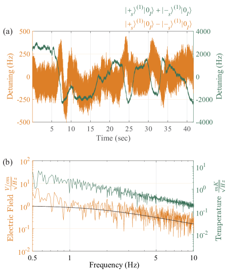
The temperature fluctuations are separated from the electric field fluctuations using the temperature-dependent, correlated shifts of the parameter (See Eqn. 3). The sum of the time traces corresponds to the temperature fluctuations while the difference of the time traces corresponds to the electric field fluctuations. The NSD of the resulting sum and differences shows temperature fluctuations of and electric field fluctuations of , respectively (See Fig. 4). Thus, our method shows a shot-noise-limited electric-field sensitivity that is approximately 8 improved over a measurement without deconvolution with temperature fluctuations.
IV Discussion
We have demonstrated sensing of electric fields with an ensemble of NV-s below 1 Hz with sensitivities approaching . In spite of large temperature variations, inhomogeneous distribution of strain and non-collinear orientations, our measurement technique allows for accurate measurements of the ensemble strain distribution and the ensemble average of the transverse electric susceptibility, ; both of which are needed to accurately measure low-frequency electric fields.
NV--based sensing lends itself to imaging electric fields at or below the optical diffraction limit Chen et al. (2013); Pfender et al. (2014); Hsiao et al. (2016). We anticipate that the use of low-strain nanodiamonds with our demonstrated zero-magnetic field regime would enable simultaneous monitoring of both temperature Kucsko et al. (2013) and electric fields Dolde et al. (2011). To the best of our knowledge, nanodiamonds with low-strain ( kHz) are not yet available despite the tremendous progress in improving the electronic coherence within such nano-scale structures Knowles et al. (2014); Trusheim et al. (2014). Such low-strain nanodiamonds with high densities of NV-s would be beneficial for in vitro biological studies Řehoř et al. (2016); Karaveli et al. (2016) and microelectronic diagonistics Nowodzinski et al. (2015). Finally, due to the many combinations of host materials and defects, there is significant potential in discovering defects within two- and three-dimensional materials that would further improve upon existing electronic spin-based electrometers Freysoldt et al. (2014); Tran et al. (2016).
In this work, we have demonstrated a factor of more than 200x improvement over previous demonstrations using a single NV-. The sensitivity may be further improved by using a diamond with 1000x higher densities of NV-s Barry et al. (2016), improving the photon collection efficiency by another 10-100 times by patterning the diamond surface to overcome the confinement due to total internal reflection Schell et al. (2014); Li et al. (2015), and implementing pulsed control techniques to avoid power-broadening of the transitions Hodges et al. (2013); Toyli et al. (2013); Neumann et al. (2013b); Jamonneau et al. (2016). Such readily accessible material and setup improvements could improve the shot-noise limited electric field sensitivity to . Additional coherent control on either the surrounding electron Cappellaro (2012); Bonato et al. (2016) or nuclear spins Hirose and Cappellaro (2016); Unden et al. (2016); Clevenson et al. (2016) in diamond would further improve the sensitivity by reducing the broadening of the transition line width. MW field inhomogeneities that are typically more problematic for pulsed techniques would benefit from recently proposed methodologies for generating robust pulse sequences Farfurnik et al. (2015). Other promising directions for spin-based sensing involve all-optical techniques in diamond for electrometry Wickenbrock et al. (2016).
Acknowledgements.
Acknowledgements: The authors would like to thank Paola Cappellaro, John Barry, John Cortese, Colin Bruzewicz, Florian Dolde, Carson Teale, Christopher McNally, Christopher Foy, Xiao Wang, Peter Murphy, Sinan Karaveli, Jeremy Sage, and Jonathon Sedlack for fruitful discussions. E.H.C. and H.C. were supported by NASA’s Office of Chief Technologist on the Space Technology Research Fellowship. D.E. acknowledges support by the Air Force Office of Scientific Research PECASE, supervised by Dr. Gernot Pomrenke. This material is based upon work supported by the Assistant Secretary of Defense for Research and Engineering under Air Force Contract No. FA8721-05-C-0002 and/or FA8702-15-D-0001. Any opinions, findings, conclusions or recommendations expressed in this material are those of the author(s) and do not necessarily reflect the views of the Assistant Secretary of Defense for Research and Engineering.References
- Sharma et al. (2016) S. Sharma, C. Hovde, and D. H. Beck, SPIE Proceedings 9755 (2016), 10.1117/12.2211910.
- Merceret et al. (2008) F. J. Merceret, J. G. Ward, D. M. Mach, M. G. Bateman, and J. E. Dye, Journal of Applied Meteorology and Climatology 47, 240 (2008).
- Simoes et al. (2012) F. Simoes, R. Pfaff, J.-J. Berthelier, and J. Klenzing, Space Science Reviews 168, 551 (2012), wOS:000305907900020.
- Mezuman et al. (2014) K. Mezuman, C. Price, and E. Galanti, Environmental Research Letters 9, 124023 (2014), wOS:000347454800024.
- Barry et al. (2016) J. F. Barry, M. J. Turner, J. M. Schloss, D. R. Glenn, Y. Song, M. D. Lukin, H. Park, and R. L. Walsworth, arXiv:1602.01056 [cond-mat, physics:physics, physics:quant-ph, q-bio] (2016), arXiv:1602.01056 [cond-mat, physics:physics, physics:quant-ph, q-bio] .
- Fort et al. (2011) A. Fort, M. Mugnaini, V. Vignoli, S. Rocchi, F. Perini, J. Monari, M. Schiaffino, and F. Fiocchi, Ieee Transactions on Instrumentation and Measurement 60, 2778 (2011), wOS:000293658600005.
- Riehl et al. (2003) P. S. Riehl, K. L. Scott, R. S. Muller, R. T. Howe, and J. A. Yasaitis, Journal of microelectromechanical systems 12, 577 (2003).
- Harrington (1960) R. F. Harrington, J. Res. Nat. Bur. Stand 64, 1 (1960).
- Chu (1948) L. J. Chu, Journal of Applied Physics 19, 1163 (1948).
- Chubb (2015) J. Chubb, Journal of Electrostatics 78, 1 (2015), wOS:000366780800001.
- Barr et al. (2000) R. Barr, D. L. Jones, and C. J. Rodger, Journal of Atmospheric and Solar-Terrestrial Physics 62, 1689 (NOV-DEC 2000), wOS:000166550600012.
- Savchenkov et al. (2014) A. A. Savchenkov, W. Liang, V. S. Ilchenko, E. Dale, E. A. Savchenkova, A. B. Matsko, D. Seidel, and L. Maleki, AIP Advances 4, 122901 (2014).
- Toney (2015) J. E. Toney, Lithium Niobate Photonics (Artech House, 2015).
- Vohra et al. (1991) S. T. Vohra, F. Bucholtz, and A. D. Kersey, Optics Letters 16, 1445 (1991).
- Lee et al. (2008) J. Lee, Y. Zhu, and A. Seshia, Journal of Micromechanics and Microengineering 18, 025033 (2008).
- Vincent et al. (2004) J. Vincent, V. Narayan, H. Pettersson, M. Willander, K. Jeppson, and L. Bengtsson, Journal of applied physics 95, 323 (2004).
- Neumann et al. (2013a) C. Neumann, C. Volk, S. Engels, and C. Stampfer, Nanotechnology 24, 444001 (2013a).
- Bruzewicz et al. (2015) C. D. Bruzewicz, J. M. Sage, and J. Chiaverini, Physical Review A 91, 041402 (2015).
- Osterwalder and Merkt (1999) A. Osterwalder and F. Merkt, Physical Review Letters 82, 1831 (1999).
- Sedlacek et al. (2012) J. A. Sedlacek, A. Schwettmann, H. Kübler, R. Löw, T. Pfau, and J. P. Shaffer, Nature Physics 8, 819 (2012).
- Awschalom et al. (2013) D. D. Awschalom, L. C. Bassett, a. S. Dzurak, E. L. Hu, and J. R. Petta, Science 339, 1174 (2013).
- Degen et al. (2016) C. Degen, F. Reinhard, and P. Cappellaro, arXiv preprint arXiv:1611.02427 (2016).
- Acosta and Hemmer (2013) V. Acosta and P. Hemmer, MRS Bulletin 38, 127 (2013).
- Clevenson et al. (2015) H. Clevenson, M. E. Trusheim, C. Teale, T. Schröder, D. Braje, and D. Englund, Nature Physics 11, 393 (2015).
- Fang et al. (2013) K. Fang, V. Acosta, C. Santori, Z. Huang, K. Itoh, H. Watanabe, S. Shikata, and R. Beausoleil, Physical Review Letters 110 (2013), 10.1103/PhysRevLett.110.130802.
- Dolde et al. (2011) F. Dolde, H. Fedder, M. W. Doherty, T. Nöbauer, F. Rempp, G. Balasubramanian, T. Wolf, F. Reinhard, L. C. L. Hollenberg, F. Jelezko, and J. Wrachtrup, Nature Physics 7, 459 (2011).
- Doherty et al. (2014) M. W. Doherty, J. Michl, F. Dolde, I. Jakobi, P. Neumann, N. B. Manson, and J. Wrachtrup, New Journal of Physics 16, 063067 (2014).
- Tamarat et al. (2006) P. Tamarat, T. Gaebel, J. Rabeau, M. Khan, A. Greentree, H. Wilson, L. Hollenberg, S. Prawer, P. Hemmer, F. Jelezko, and J. Wrachtrup, Physical Review Letters 97 (2006), 10.1103/PhysRevLett.97.083002.
- Note (1) See Supplemental Material at [URL will be inserted by publisher] for this projected sensitivity using values from recent magnetometry experiments Barry et al. (2016).
- Plakhotnik et al. (2014) T. Plakhotnik, M. W. Doherty, J. H. Cole, R. Chapman, and N. B. Manson, Nano Letters 14, 4989 (2014).
- Doherty et al. (2013) M. W. Doherty, N. B. Manson, P. Delaney, F. Jelezko, and L. C. L. Hollenberg, Physics Reports 528, 1 (2013).
- Note (2) See Doherty et al. (2014) for the relationship between electric-dipole moment, and the electric susceptibility, .
- Note (3) See Fig. 7 for the differences and similarities in using the ground and excited states of the NV-for electrometry.
- Chen et al. (2011) X.-D. Chen, C.-H. Dong, F.-W. Sun, C.-L. Zou, J.-M. Cui, Z.-F. Han, and G.-C. Guo, Applied Physics Letters 99, 161903 (2011).
- Note (4) .
- Note (5) See Supplemental Material at [URL will be inserted by publisher] for an analysis considering the isotropic distribution of strain with an ensemble of NV-s.
- Note (6) See Supplemental Material at [URL will be inserted by publisher] for a description of the technical details of the setup.
- Chen et al. (2013) E. H. Chen, O. Gaathon, M. E. Trusheim, and D. Englund, Nano Letters 13, 2073 (2013).
- Pfender et al. (2014) M. Pfender, N. Aslam, G. Waldherr, P. Neumann, and J. Wrachtrup, Proceedings of the National Academy of Sciences 111, 14669 (2014).
- Hsiao et al. (2016) W. W.-W. Hsiao, Y. Y. Hui, P.-C. Tsai, and H.-C. Chang, Accounts of Chemical Research (2016), 10.1021/acs.accounts.5b00484.
- Kucsko et al. (2013) G. Kucsko, P. C. Maurer, N. Y. Yao, M. Kubo, H. J. Noh, P. K. Lo, H. Park, and M. D. Lukin, Nature 500, 54 (2013).
- Knowles et al. (2014) H. S. Knowles, D. M. Kara, and M. Atatüre, Nature Materials 13, 21 (2014).
- Trusheim et al. (2014) M. E. Trusheim, L. Li, A. Laraoui, E. H. Chen, H. Bakhru, T. Schröder, O. Gaathon, C. A. Meriles, and D. Englund, Nano Letters 14, 32 (2014).
- Řehoř et al. (2016) I. Řehoř, J. Šlegerová, J. Havlík, H. Raabová, J. Hývl, E. Muchová, and P. Cígler, in Carbon Nanomaterials for Biomedical Applications, Springer Series in Biomaterials Science and Engineering No. 5, edited by M. Zhang, R. R. Naik, and L. Dai (Springer International Publishing, 2016) pp. 319–361.
- Karaveli et al. (2016) S. Karaveli, O. Gaathon, A. Wolcott, R. Sakakibara, O. A. Shemesh, D. S. Peterka, E. S. Boyden, J. S. Owen, R. Yuste, and D. Englund, Proceedings of the National Academy of Sciences , 201504451 (2016).
- Nowodzinski et al. (2015) A. Nowodzinski, M. Chipaux, L. Toraille, V. Jacques, J.-F. Roch, and T. Debuisschert, Microelectronics Reliability 55, 1549 (2015).
- Freysoldt et al. (2014) C. Freysoldt, B. Grabowski, T. Hickel, J. Neugebauer, G. Kresse, A. Janotti, and C. G. Van de Walle, Reviews of Modern Physics 86, 253 (2014).
- Tran et al. (2016) T. T. Tran, C. Zachreson, A. M. Berhane, K. Bray, R. G. Sandstrom, L. H. Li, T. Taniguchi, K. Watanabe, I. Aharonovich, and M. Toth, Physical Review Applied 5, 034005 (2016).
- Schell et al. (2014) A. W. Schell, T. Neumer, Q. Shi, J. Kaschke, J. Fischer, M. Wegener, and O. Benson, Applied Physics Letters 105, 231117 (2014).
- Li et al. (2015) L. Li, E. H. Chen, J. Zheng, S. L. Mouradian, F. Dolde, T. Schröder, S. Karaveli, M. L. Markham, D. J. Twitchen, and D. Englund, Nano Letters 15, 1493 (2015).
- Hodges et al. (2013) J. Hodges, N. Yao, D. Maclaurin, C. Rastogi, M. Lukin, and D. Englund, Physical Review A 87 (2013), 10.1103/PhysRevA.87.032118.
- Toyli et al. (2013) D. M. Toyli, C. F. de las Casas, D. J. Christle, V. V. Dobrovitski, and D. D. Awschalom, Proceedings of the National Academy of Sciences 110, 8417 (2013).
- Neumann et al. (2013b) P. Neumann, I. Jakobi, F. Dolde, C. Burk, R. Reuter, G. Waldherr, J. Honert, T. Wolf, A. Brunner, J. H. Shim, D. Suter, H. Sumiya, J. Isoya, and J. Wrachtrup, Nano Letters 13, 2738 (2013b).
- Jamonneau et al. (2016) P. Jamonneau, M. Lesik, J. Tetienne, I. Alvizu, L. Mayer, A. Dréau, S. Kosen, J.-F. Roch, S. Pezzagna, J. Meijer, et al., Physical Review B 93, 024305 (2016).
- Cappellaro (2012) P. Cappellaro, Physical Review A 85, 030301 (2012).
- Bonato et al. (2016) C. Bonato, M. S. Blok, H. T. Dinani, D. W. Berry, M. L. Markham, D. J. Twitchen, and R. Hanson, Nature nanotechnology 11, 247 (2016).
- Hirose and Cappellaro (2016) M. Hirose and P. Cappellaro, Nature 532, 77 (2016).
- Unden et al. (2016) T. Unden, P. Balasubramanian, D. Louzon, Y. Vinkler, M. B. Plenio, M. Markham, D. Twitchen, A. Stacey, I. Lovchinsky, A. O. Sushkov, et al., Physical Review Letters 116, 230502 (2016).
- Clevenson et al. (2016) H. A. Clevenson, E. H. Chen, F. Dolde, C. Teale, D. Englund, and D. Braje, Phys. Rev. A 94, 021401 (2016).
- Farfurnik et al. (2015) D. Farfurnik, A. Jarmola, L. M. Pham, Z.-H. Wang, V. V. Dobrovitski, R. L. Walsworth, D. Budker, and N. Bar-Gill, Physical Review B 92, 060301 (2015).
- Wickenbrock et al. (2016) A. Wickenbrock, H. Zheng, L. Bougas, N. Leefer, S. Afach, A. Jarmola, V. M. Acosta, and D. Budker, arXiv preprint arXiv:1606.03070 (2016).
Appendix A Supplementary Information
A.1 Addressing an ensemble of NV-s
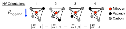
A diagram showing four of the eight possible NV- orientations found with a diamond containing an ensemble of NV-s (See Fig. 5).
A.2 Sensitivity approaching
Using Eqn. 4 in the main text, we expect a shot-noise-limited sensitivity approaching
using photocurrent values of 10 mW ( eV/sec 1 photon/1.9eV = photon/sec) as typically seen with ensemble NV- measurements for magnetometry experiments [5], a transverse electric susceptibility of , line width () of 1 MHz, and contrast() of 0.05.
A.3 Full energy transition expression
Using second-order, degenerate perturbation theory, we derive the microwave transition frequencies between the eigenstates split by transverse electric fields:
| (5) |
where , , , , , and .
The equation which describes the ensemble ODMR spectrum is given by:
| (6) |
where is the frequency of the applied MW field, is the ensemble average of the ODMR contrast, is the ensemble average of the crystal field, is the (2,1) Gamma probability distribution of the strain magnitude, is the ensemble average of the strain magnitude, is the full-width half-maximum of single-NV line-widths, denotes the strain vector’s altitude angle away from the NV- symmetry axis, and is the strain vector’s azimuthal angle.
A.4 Zero-ing of magnetic field using gradient descent
It is possible to zero the magnetic field using gradient descent because the overlap of the transitions of all eight orientations of NV-s has a contrast that varies smoothly with respect to applied small magnetic fields. By taking local gradients of the contrast at each magnetic field setting (, and ) followed by successively smaller step sizes, we find the setting of that achieves the globally maximum ODMR contrast and hence a zero magnetic field.
A.5 Digital Lock-In Amplifier Implementation
Using an FPGA high speed DAC, our system contains both the waveform generation and lock-in detection to perform readout of the optical signals from the diamond. The MW waveform sent to the diamond is generated digitally in the FPGA by direct-sampling with a high-speed DAC (2.4 Giga-samples, 3rd nyquist zone), which significantly simplifies the RF hardware and allows generation of arbitrary waveforms. Control is performed by a Linux based Python TCP/IP server running on the Zynq’s ARM processor that interfaces to MATLAB on the control PC.
A.6 Bandwidth limitations of the NV-based electrometer
The mechanism that determines the NV spin’s sensitivity to high frequency electric fields at room temperature is limited by the spin-dependent readout rate. This rate is limited by the intersystem crossing process which is weakly temperature dependent due to its non-spin conserving property, and is 1/300 ns. Due to current experimental constraints such as limited photon collection efficiency and a limited bandwidth of the photodiode given the large dynamic range needed, the time constant on the LIA can then be set to match the bandwidth of the NV electrometer’s spin readout of 3 MHz. Higher detection bandwidths can be achieved using single-shot spin readout at cryogenic temperatures.
A.7 Excited-state optically detected magnetic resonance
The spin physics of the NV-’s excited state is identical with the NV-’s ground state at temperatures above approximately 50 Kelvin [25]. For purposes of sensing electric fields, the excited state is expected to be significantly less effective despite having 20 greater transverse field sensitivity. This is attributed to shorter optical spontaneous lifetime (12 ns) and smaller ODMR contrast in the excited state. This analysis can be validated by substituting values from Fig. 7 into Eqn. 4.