Influence of magnetic field and ferromagnetic film thickness on domain pattern transfer in multiferroic heterostructures
Abstract
We report on domain pattern transfer from a ferroelectric BaTiO3 substrate to a CoFeB wedge film with a thickness of up to 150 nm. Strain coupling to domains in BaTiO3 induces a regular modulation of uniaxial magnetic anisotropy in CoFeB via an inverse magnetostriction effect. As a result, the domain structures of the CoFeB wedge film and BaTiO3 substrate correlate fully and straight ferroelectric domain boundaries in BaTiO3 pin magnetic domain walls in CoFeB. We use x-ray photoemission electron microscopy and magneto-optical Kerr effect microscopy to characterize the spin structure of the pinned domain walls. In a rotating magnetic field, abrupt and reversible transitions between two domain wall types occur, namely, narrow walls where the magnetization vectors align head-to-tail and much broader walls with alternating head-to-head and tail-to-tail magnetization configurations. We characterize variations of the domain wall spin structure as a function of magnetic field strength and CoFeB film thickness and compare the experimental results with micromagnetic simulations.
I Introduction
Magnetic patterning refers to any method that induces controlled variations of magnetic properties in a continuous ferromagnetic film without topographic structuring. It allows for the creation of regular patterns of magnetic domains and domain walls, defining magnetic responses that would not occur in magnetically uniform films. Several techniques are available for magnetic patterning. These include focused ion beam irradiation Chappert et al. (1998); Fassbender and McCord (2008); Franken et al. (2012); Hamann et al. (2014), low-energy proton irradiation Kim et al. (2012), oxygen ion migration from an adjacent metal-oxide layer Bauer et al. (2013, 2015), and thermally-assisted scanning probe lithography Albisetti et al. (2016). Interface coupling in multiferroic heterostructures can also be used to tailor the properties of ferromagnetic films. Exchange coupling to domains in a multiferroic BiFeO3 layer Chu et al. (2008); Lebeugle et al. (2009); Heron et al. (2011); You et al. (2013); Heron et al. (2014) or strain coupling to ferroelastic domains in a BaTiO3 crystal Lahtinen et al. (2011, 2012a, 2012b); Chopdekar et al. (2012); Streubel et al. (2013); Ghidini et al. (2015); Franke et al. (2015); Shirahata et al. (2015), for instance, induce lateral modulations of magnetic anisotropy in the adjacent ferromagnetic film. If the modulations of magnetic anisotropy are strong enough, one-to-one correlations between domain patterns in the ferroelectric and ferromagnetic layers are attained. Full domain pattern transfer in multiferroic heterostructures enables electric-field induced magnetic switching Chu et al. (2008); Lebeugle et al. (2009); Heron et al. (2011, 2014); Lahtinen et al. (2011, 2012a); Ghidini et al. (2015); Shirahata et al. (2015) and reversible magnetic domain wall motion Lahtinen et al. (2012a); Franke et al. (2015), offering promising prospects for low-power spintronic devices.
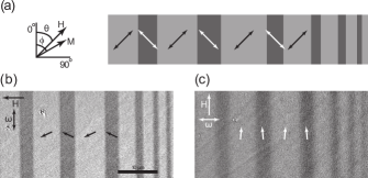
Here, we investigate how domain pattern transfer from a ferroelectric BaTiO3 substrate to a CoFeB wedge film varies with ferromagnetic film thickness and applied magnetic field. In our experiments, the BaTiO3 substrate consists of stripe domains with in-plane ferroelectric polarization. At the domain boundaries, the polarization rotates abruptly by 90∘. Since the BaTiO3 crystal is tetragonal at room temperature, rotation of the ferroelectric polarization also reorients the axis of lattice tetragonality. Via inverse magnetostriction, this induces regular modulations of uniaxial magnetic anisotropy in the CoFeB wedge film, as illustrated in Fig. 1(a). Consequently, the ferroelectric stripe domain pattern in the BaTiO3 substrate is fully transferred to the CoFeB wedge film and the strain-induced rotations of uniaxial magnetic anisotropy at the ferroelectric domain boundaries firmly pin the magnetic domain walls. Magnetic domain walls are therefore as straight as their ferroelectric counterpart and do not move in a magnetic field. The latter effect enables active switching between two types of magnetic domain walls Franke et al. (2012). Domain walls with a head-to-tail alignment of magnetization form when an in-plane magnetic field is applied perpendicular to the stripe domains (Fig. 1(b)). The energy and width of these walls are determined mostly by the strength of exchange interactions and magnetic anisotropy. An in-plane magnetic field parallel to the stripe domains, on the other hand, initializes domain walls with alternating head-to-head and tail-to-tail magnetization configurations (Fig. 1(c)). Being defined by magnetic anisotropy and long-range magnetostatic interactions (i.e. magnetic charges), these magnetic domain walls are much wider and higher in energy than the head-to-tail walls. Hereafter, we will refer to the two domain-wall types as magnetically charged (head-to-head and tail-to-tail) and uncharged (head-to-tail).
The width and energy of pinned magnetic domain walls affects domain pattern transfer and magnetic switching in multiferroic heterostructures Franke et al. (2014); Casiraghi et al. (2015). Breakdown of pattern transfer occurs when the width of magnetic domain walls and ferroelectric stripe domains become comparable. More specifically, in the strain-coupled CoFeB/BaTiO3 system we consider here, the rotation of magnetization between neighboring domains in zero magnetic field decreases from 90∘ for wide ferroelectric stripe domains to nearly 0∘ for very narrow domains. As the widths of charged and uncharged magnetic domain walls differ significantly (up to about two orders of magnitude in thick ferromagnetic films), magnetic switching from one domain wall type to the other changes the amount of magnetization rotation between domains and, thereby, the magnetic contrast. An example is shown in Figs. 1(b) and (c). The magneto-optical Kerr effect (MOKE) microscopy images in these figures are recorded on a sample area where the CoFeB wedge film is 150 nm thick. In (b), a 40 mT in-plane magnetic field is oriented perpendicular to the stripe domains. The uncharged magnetic domain walls that form are much narrower than the stripe domains and, consequently, a sizeable rotation of magnetization between domains and clear magnetic contrast are obtained. In (c), the in-plane magnetic field is rotated by 90∘. Now, much wider charged domain walls separate the stripe domains and the magnetization in the CoFeB film is more uniform, particularly for the narrow stripe domains on the right. Rotation of an external magnetic field thus causes the consecutive writing and erasure of magnetic stripe patterns, as previously discussed in Ref. 23. In this paper, we report on the variation of domain pattern transfer with ferromagnetic film thickness and the strength and orientation of applied magnetic field. Experimentally, we measure the evolution of magnetic domain patterns in a rotating magnetic field. From these measurements we derive , where and indicate the angles of magnetization in two neighboring stripe domains. Large values of thus represent robust domain pattern transfer. We use micromagnetic simulations to interpret our experimental data.
II Methods
For the experiments we grew a Co40Fe40B20 wedge film, with thickness up to 150 nm, onto a BaTiO3 substrate. The film was sputtered at 300 ∘C and capped with 3 nm Au to prevent oxidation. At this deposition temperature the BaTiO3 substrate is paraelectric and its crystal structure is cubic. The ferroelectric and ferromagnetic stripe domains are formed during post-deposition cooling through the BaTiO3 paraelectric-to-ferroelectric phase transition at C. This procedure resulted in one-to-one domain correlations across the entire CoFeB wedge film. We used MOKE microscopy to image the magnetic stripe domains in a slowly rotating in-plane magnetic field. High-resolution images of the magnetic domains were obtained by x-ray photoemission electron microscopy (PEEM) on beamline UE49-PGM1 at the BESSY II synchrotron facility. Illumination at oblique incidence and x-ray magnetic circular dichroism (XMCD) at the Fe L3 edge were used to visualize the direction of in-plane magnetization with a spatial resolution of about 30 nm. Micromagnetic simulations were performed in MuMax3 Vansteenkiste et al. (2014). In the simulations, the width of the stripe domains was set to 3 m and the simulation area was discretized into nm3 cells. As input parameters we used a uniaxial magnetic anisotropy J/m3 (derived from MOKE measurements), a saturation magnetization A/m, and an exchange constant J/m.
III Results and discussion
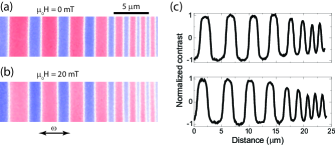
Figure 2 shows PEEM images of the CoFeB film (a) at remanence and (b) under an in-plane magnetic field of 20 mT. In these experiments, charged domain walls separate the magnetic stripe domains and the CoFeB film is 150 nm thick. From line profiles on wide domains (Fig. 2(c)), we extract a domain wall width of 2.0 m for mT and 2.1 m for mT. Because of the large width of charged domain walls, the magnetic contrast reduces considerably in the narrow stripe domains on the right side of the PEEM images. This finite-size scaling effect is slightly more pronounced for mT, which confirms the notion that wider domain walls cause a stronger reduction of magnetization rotation in narrow domains.
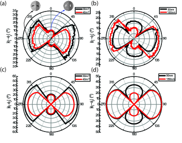
Next, we investigate the effect of a rotating in-plane magnetic field on domain pattern transfer. In the experiments, MOKE microscopy images are recorded as a function of magnetic field angle . From the series of images we extract the orientation of magnetization ( and ) in two neighboring stripe domains. The stripe domains are 3 - 4 m wide. Figures 3(a) and (b) show results for a rotating magnetic field of 30 mT and 40 mT and a CoFeB film thickness of 50 nm and 150 nm. In all cases, transitions between small and larger values of are measured. These switching events, which signify a change in magnetic contrast (see Fig. 1), are caused by abrupt domain wall transformations. Starting from , the stripe domains are initially separated by broad charged domain walls. The rotation of magnetization between neighboring domains is thus small. Clockwise rotation of a constant magnetic field switches the magnetization of every second stripe domain at . As a result, the broad charged domain walls transform into narrow uncharged domain walls. This increases and, consequently, the magnetic contrast of MOKE microscopy images. At , a second switching event restores the charged domain walls, causing a reduction of . Back and forth switching between the two types of domain walls continues upon further rotation of the magnetic field. For narrow uncharged domain walls, the ferroelectric stripe domain pattern in the BaTiO3 substrate is clearly transferred to the CoFeB wedge. Broad charged domain walls, on the other hand, lead to nearly uniform magnetization in the CoFeB film. Results from micromagnetic simulations, shown in Figs. 3(c) and (d), qualitatively confirm the measurements. While the shape of the switching curves is nearly identical, the magnitude of is larger in the simulations. The main reason for this is a difference in data acquisition. In order to increase the signal to noise ratio in the experimental data, we extract the average direction of magnetization in two neighboring stripe domains, while simulated data is collected at the two domain centers.
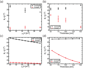
Figure 4 summarizes the dependence of on applied magnetic field and CoFeB film thickness. With increasing field, the magnetization rotates towards the field axis. The resulting reduction in the rotation of magnetization between neighboring stripe domains is more pronounced for uncharged domain walls. The effect of CoFeB film thickness is opposite for the two types of magnetic domain walls. The width of charged domain walls increases with ferromagnetic film thickness due to stronger magnetostatic interactions. For charged walls, the width is given by Hubert (1979). Although the exact profile of charged domain walls changes upon a reduction of magnetization rotation, the width of smaller-angle walls does also increase with ferromagnetic film thickness. Wider charged domain walls on the thick side of the CoFeB wedge film significantly reduce and, thus, the degree of domain pattern transfer. We measure and simulate a much smaller and opposite effect for uncharged domain walls. While the spin structure of these narrow walls is mostly determined by the strength of exchange interactions and uniaxial magnetic anisotropy, magnetostatic interactions slightly reduce their width in thick films Franke et al. (2014). This effect enhances the rotation of magnetization between neighboring domains, in agreement with the data of Figs. 4(b) and (d).
Finally, we use micromagnetic simulations to estimate how the width of pinned magnetic domain walls in our CoFeB/BaTiO3 multiferroic heterostructure varies as a function of magnetic field angle. We define the domain wall width as Franke et al. (2014)
| (1) |
where is the reduced magnetization angle
| (2) |
and and are the angles of magnetization in the centers of two neighboring stripe domains. For zero magnetic field and a CoFeB film thickness of 150 nm, we simulate a width of 25 nm and 1.9 m for uncharged and charged domain walls, respectively, a difference of nearly two orders of magnitude. The width of charged magnetic domain walls agrees well with the PEEM measurements of Fig. 2.
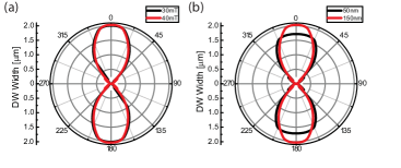
Figure 5 shows the variation of domain wall width in a rotating in-plane magnetic field. The widest domain walls are obtained if the magnetic field is aligned parallel to the stripe domains. Rotation of the magnetic field away from this position reduces the width of these charged domain walls. At , a transformation to much narrower uncharged domain walls occurs. Back and forth switching between the two types of domain walls in a rotating magnetic field changes the wall width by about two orders of magnitude for nm. Thus, while the walls remain firmly pinned onto the ferroelectric boundaries in the BaTiO3 substrate, the magnetic field tunes their spin structure and width. As a result, clear imprinting of narrow BaTiO3 stripe domains into the CoFeB film occurs only if the magnetic domain walls are uncharged.
In conclusions, we have studied domain pattern transfer from a ferroelectric BaTiO3 substrate to a ferromagnetic CoFeB wedge film using MOKE microscopy, x-ray PEEM, and micromagnetic simulations. This strain-coupled multiferroic system is characterized by strong pinning of magnetic domain walls onto ferroelectric boundaries. Using a rotating magnetic field, we have demonstrated that the width of pinned magnetic domain walls can be tuned by two orders of magnitude. Switching from narrow uncharged domain walls to broad charged domain walls deteriorates the transfer of domain patterns, which is reflected by a decrease of magnetic contrast in MOKE microscopy images. The weakest magnetic contrast is obtained when the stripe domains are narrow and the CoFeB film is thick.
IV Acknowledgments
This work was supported by the European Research Council (ERC-2012-StG 307502-E-CONTROL and ERC-2014-PoC 665215-EMOTION).
References
- Chappert et al. (1998) C. Chappert, H. Bernas, J. Ferre, V. Kottler, J.-P. Jamet, Y. Chen, E. Cambril, T. Devolder, F. Rousseaux, V. Mathet, and H. Launois, Science 280, 1919 (1998).
- Fassbender and McCord (2008) J. Fassbender and J. McCord, Journal of Magnetism and Magnetic Materials 320, 579 (2008).
- Franken et al. (2012) J. H. Franken, H. J. M. Swagten, and B. Koopmans, Nature Nanotechnology 7, 499 (2012).
- Hamann et al. (2014) C. Hamann, R. Mattheis, I. Mönch, J. Fassbender, L. Schultz, and J. McCord, New Journal of Physics 16, 023010 (2014).
- Kim et al. (2012) S. Kim, S. Lee, J. Ko, J. Son, M. Kim, S. Kang, and J. Hong, Nature Nanotechnology 7, 567 (2012).
- Bauer et al. (2013) U. Bauer, S. Emori, and G. S. D. Beach, Nature Nanotechnology 8, 411 (2013).
- Bauer et al. (2015) U. Bauer, L. Yao, A. J. Tan, P. Agrawal, S. Emori, H. L. Tuller, S. van Dijken, and G. S. D. Beach, Nature Materials 14, 174 (2015).
- Albisetti et al. (2016) E. Albisetti, D. Petti, M. Pancaldi, M. Madami, S. Tacchi, J. Curtis, W. P. King, A. Papp, G. Csaba, W. Porod, P. Vavassori, E. Riedo, and R. Bertacco, Nature Nanotechnology 11, 545 (2016).
- Chu et al. (2008) Y.-H. Chu, L. W. Martin, M. B. Holcomb, M. Gajek, S.-J. Han, Q. He, N. Balke, C.-H. Yang, D. Lee, W. Hu, Q. Zhan, P.-L. Yang, A. Fraile-Rodríguez, A. Scholl, S. X. Wang, and R. Ramesh, Nature Materials 7, 478 (2008).
- Lebeugle et al. (2009) D. Lebeugle, A. Mougin, M. Viret, D. Colson, and L. Ranno, Physical Review Letters 103, 257601 (2009).
- Heron et al. (2011) J. T. Heron, M. Trassin, K. Ashraf, M. Gajek, Q. He, S. Y. Yang, D. E. Nikonov, Y.-H. Chu, S. Salahuddin, and R. Ramesh, Physical Review Letters 107, 217202 (2011).
- You et al. (2013) L. You, B. Wang, X. Zou, Z. S. Lim, Y. Zhou, H. Ding, L. Chen, and J. Wang, Physical Review B 88, 184426 (2013).
- Heron et al. (2014) J. T. Heron, J. L. Bosse, Q. He, Y. Gao, M. Trassin, L. Ye, J. D. Clarkson, C. Wang, J. Liu, S. Salahuddin, D. C. Ralph, D. G. Schlom, J. Íñiguez, B. D. Huey, and R. Ramesh, Nature 516, 370 (2014).
- Lahtinen et al. (2011) T. H. E. Lahtinen, J. O. Tuomi, and S. van Dijken, Advanced Materials 23, 3187 (2011).
- Lahtinen et al. (2012a) T. H. E. Lahtinen, K. J. A. Franke, and S. van Dijken, Scientific Reports 2, 258 (2012a).
- Lahtinen et al. (2012b) T. H. E. Lahtinen, Y. Shirahata, L. Yao, K. J. A. Franke, G. Venkataiah, T. Taniyama, and S. van Dijken, Applied Physics Letters 101, 262405 (2012b).
- Chopdekar et al. (2012) R. V. Chopdekar, V. K. Malik, A. Fraile Rodríguez, L. Le Guyader, Y. Takamura, A. Scholl, D. Stender, C. W. Schneider, C. Bernhard, F. Nolting, and L. J. Heyderman, Physical Review B 86, 014408 (2012).
- Streubel et al. (2013) R. Streubel, D. Köhler, R. Schäfer, and L. M. Eng, Physical Review B 87, 054410 (2013).
- Ghidini et al. (2015) M. Ghidini, F. Maccherozzi, X. Moya, L. C. Phillips, W. Yan, J. Soussi, N. Métallier, M. E. Vickers, N. J. Steinke, R. Mansell, C. H. W. Barnes, S. S. Dhesi, and N. D. Mathur, Advanced Materials 27, 1460 (2015).
- Franke et al. (2015) K. J. A. Franke, B. Van de Wiele, Y. Shirahata, S. J. Hämäläinen, T. Taniyama, and S. van Dijken, Physical Review X 5, 011010 (2015).
- Shirahata et al. (2015) Y. Shirahata, R. Shiina, D. López González, K. J. A. Franke, E. Wada, M. Itoh, N. A. Pertsev, S. van Dijken, and T. Taniyama, NPG Asia Materials 7, e198 (2015).
- Franke et al. (2012) K. J. A. Franke, T. H. E. Lahtinen, and S. van Dijken, Physical Review B 85, 094423 (2012).
- Franke et al. (2014) K. J. A. Franke, D. López González, S. J. Hämäläinen, and S. van Dijken, Physical Review Letters 112, 017201 (2014).
- Casiraghi et al. (2015) A. Casiraghi, T. Rincón Domínguez, S. Rößler, K. J. A. Franke, D. López González, S. J. Hämäläinen, R. Frömter, H. P. Oepen, and S. van Dijken, Physical Review B 92, 054406 (2015).
- Vansteenkiste et al. (2014) A. Vansteenkiste, J. Leliaert, M. Dvornik, M. Helsen, F. Garcia-Sanchez, and B. Van Waeyenberge, AIP Advances 4, 107133 (2014).
- Hubert (1979) A. Hubert, IEEE Trans. Magn. 15, 1251 (1979).