Reconfigurable re-entrant cavity for wireless coupling to an electro-optomechanical device
Abstract
An electro-optomechanical device capable of microwave-to-optics conversion has recently been demonstrated, with the vision of enabling optical networks of superconducting qubits. Here we present an improved converter design that uses a three-dimensional (3D) microwave cavity for coupling between the microwave transmission line and an integrated LC resonator on the converter chip. The new design simplifies the optical assembly and decouples it from the microwave part of the setup. Experimental demonstrations show that the modular device assembly allows us to flexibly tune the microwave coupling to the converter chip while maintaining small loss. We also find that electromechanical experiments are not impacted by the additional microwave cavity. Our design is compatible with a high-finesse optical cavity and will improve optical performance.
Quantum information networks will likely combine several disparate physical systems, exploiting their different advantages Wallquist et al. (2009). Using superconducting circuits to process and store information and optical fields to transmit it over long distances provides a promising possible realization Barends et al. (2014); Leghtas et al. (2015); Reagor et al. (2016); Ma et al. (2012); Tsang (2010); Safavi-Naeini and Painter (2011); Regal and Lehnert (2011). A key enabling technology for such a vision is a quantum state preserving electro-optic converter Tsang (2010); Safavi-Naeini and Painter (2011). A particular challenge lies in coupling the converter to propagating modes, which can transport information between nodes in the network. When addressing this challange, both the optical and microwave ports of the device must be considered.
Reliable optical connectivity requires easy assembly of the components and high optical stability, especially when cooling to cryogenic temperatures. For superconducting microwave circuits, one problem lies in coupling an electrical circuit to a microwave transmission line without also introducing undesirable coupling to other modes or otherwise spoiling the system’s coherence Axline et al. (2016). A solution is to place a chip-based, integrated circuit inside a 3D microwave cavity, which is then coupled to a transmission line. This approach has already been used successfully for several potential components of quantum information networks, such as superconducting qubits Paik et al. (2011); Rigetti et al. (2012), Josephson parametric amplifiers Narla et al. (2014), and quantum electromechanics Yuan et al. (2015); Noguchi et al. (2016).
Microwave-optics conversion has recently been demonstrated with an electro-optomechanical device, enabling a conversion efficiency of 10 % for classical signals with the prospect of quantum state transfer in the future Andrews et al. (2014). The efficiency was limited by the optical performance, which was lower than in the best pure optomechanics experiments Peterson et al. (2016). A likely source of this problem was the complex device assembly and direct connection of the transducer chip to a microwave transmission line.
In this work, we overcome these difficulties by creating a more compact, more robust system in which the optical, electrical inductor-capacitor (LC) and mechanical resonators are located inside a re-entrant microwave cavity. The modular structure of the device decouples the microwave and optical parts of the assembly. We expect this to simplify the optical alignment and ensure higher optical stability during thermal cycling. In addition, the device allows for a reduction of the mirror spacing from 5 mm to 1.2 mm, which enables a 4-fold increase of the optomechanical coupling rate Aspelmeyer, Kippenberg, and Marquardt (2014).
On the microwave side, the 3D cavity allows for precise control of the coupling between the transmission line and the chip. Cryogenic measurements at 4 K show that the coupling rate between the microwave transmission line and the superconducting LC circuit can be varied by more than one order of magnitude around the desired value, which permits high flexibility when tuning the experimental parameters. With further cooling to millikelvin temperatures, we show that the energy decay of the LC is dominated by coupling to the transmission line - as required for quantum state preservation - with only 17 % of the total loss arising from dissipation. Finally, we show that electromechanical measurements can readily be performed with the device. Our approach extends the advantages of 3D microwave cavities to a crucial quantum device and opens the path to integrate an electro-optic converter with other devices that use such cavities.
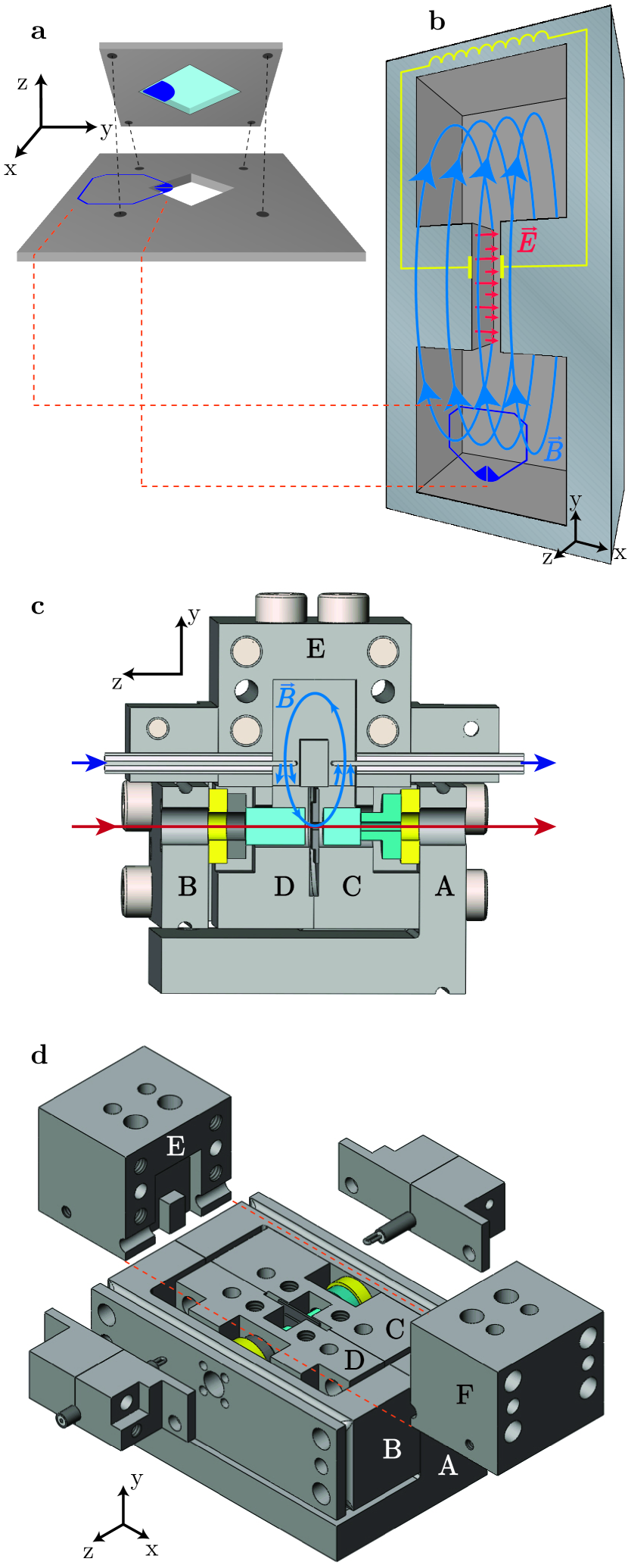
The microwave-to-optics transducer chip, shown in Fig. 1a, consists of a thin membrane that couples to the electromagnetic modes of both a microwave LC resonator and an optical Fabry-Pérot resonator. The partially metallized portion of the membrane is part of a superconducting LC circuit and forms a mechanically compliant capacitor plate. A displacement of the membrane shifts the resonant frequency of the circuit, which couples the mechanical and microwave modes. In the complete conversion setup, the membrane is additionally placed inside of an optical, high-finesse Fabry-Pérot cavity. This forms an optomechanical system and enables bidirectional conversion between the microwave and optical fields Andrews et al. (2014). The work presented here, however, solely concentrates on measurements of the microwave portion of the device.
A re-entrant microwave cavity is engineered to create a reconfigurable, effective coupling between the LC circuit and the transmission line, but without coupling substantially to other modes or sources of loss. For microwave testing purposes, the device is made out of aluminum. For experiments that also require optical stability, we would choose copper coated invar, which minimizes thermal contraction while maintaining acceptable microwave performance. The magnetic field of the cavity mode couples inductively to the chip circuit, as shown in Fig. 1b. The cavity also couples to external microwave ports via loop antennas. The cavity can be modeled as an effective LC circuit, where the capacitance depends on the dimensions of the center posts. By changing the post separation, we can thus control the microwave cavity frequency and effective coupling without otherwise disturbing the superconducting circuit or optical cavity.
Fig. 1c presents the integration of the microwave cavity with an optical Fabry-Pérot cavity. Piezoelectric crystals are mounted outside of the microwave cavity volume. They allow for adjustments of the optical cavity length and of the membrane position along the standing wave light field. The exploded view in Fig. 1d shows how the microwave and optical parts of the device have been decoupled. This greatly reduces the complexity of the setup. The optical cavity and membrane on the chip can now be aligned and assembled in the same way as a pure optomechanics system Purdy et al. (2012). The small number of interfaces and symmetric design of the mount are expected to minimize misalignment that arises from thermal contraction. Parts E-F, dubbed the “hat” of the microwave cavity, contain the center posts and connect the device to the microwave circuitry via coaxial loop couplers. We can readily change to a hat with different center post separation without interfering with any other part of the device. The external coupling can also be adjusted by changing the size of the loop couplers. In this way, we have precise control over the microwave cavity’s resonant frequency and coupling to the external ports.
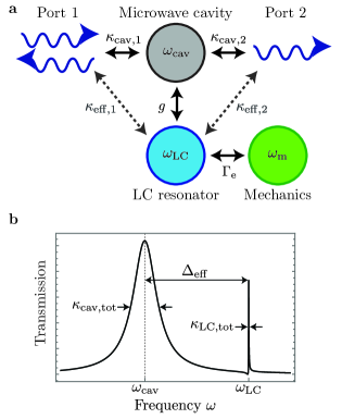
Fig. 2a outlines the relevant coupling rates of the 3D microwave cavity and electromechanical chip. The cavity has two ports and couples to them with external coupling rates and , respectively. The coupling rates are chosen such that . In this way, transmission and reflection measurements can be performed while minimizing the signal that is lost in reflection. In addition, there is an internal cavity loss rate due to absorption and radiation through seams. In total, energy stored in the cavity decays at the rate . The inductive coupling rate between the cavity and LC is quantified by the frequency . It depends on the size and position of the LC circuit’s loop inside the re-entrant cavity. The external and inductive coupling rates can be estimated by finite element simulations to guide the design process 111The electromagnetic structure solver Ansys HFSS 15.0 is used.
The coupling of the re-entrant microwave cavity mode to both the transmission line and the LC circuit gives rise to an effective, wireless coupling of the external microwave ports to the LC circuit. The cavity resonant frequency and the LC resonator frequency have been shifted from their bare values by the coupling, and their effective detuning is . For sufficient detuning , the effective coupling of the LC circuit to the cavity ports is given by
| (1) |
where . We call the couplings , to the transmission line “wireless” because there is no direct connection of the LC circuit to a waveguide or coaxial cable. Note that the effective coupling leads to an LC dissipation rate that is higher than the bare loss rate of the circuit.
The design targets an effective coupling in the 1.5-2.0 MHz range. In this way, the LC circuit is well overcoupled with respect to its expected internal loss rate, which in earlier cryogenic measurements at 4 K on a similar LC circuit was measured at 0.37 MHz Andrews et al. (2014). The total LC decay rate then also fulfills the resolved sideband criterion: , where the chip is designed to have a mechanical resonance frequency . The last inequality ensures that electro-optic conversion occurs without photon number gain, as required for quantum state preservation. From Eq. (1) we understand that we need to couple the re-entrant cavity strongly to both the LC circuit and the transmission line. In particular, the re-entrant cavity should couple to port 1 much more strongly than it couples to its internal loss such that most of the LC decay is due to its coupling to the transmission line: . Finite element simulations show that an inductive coupling MHz and external coupling to port 1 can be achieved. We know from Eq. (1) that the desired effective coupling then requires a detuning .
Fig. 2b shows the theoretical transmission spectrum of the device. The cavity and LC resonator appear as peaks at their respective resonant frequencies. The full width at half maximum (FWHM) of the Lorentzian peak centered around the cavity frequency is given by the total cavity loss rate . The second peak at frequency results from the wireless coupling. It is much narrower and has an asymmetry that depends on the cavity-LC coupling rate . The FWHM is approximately given by the total LC decay rate .
In order to test the wireless microwave coupling concept and its compatibility with electro-optomechanics experimentally, we measure the microwave response of the device. Furthermore, we demonstrate its modular, reconfigurable nature by measuring this response with several different microwave cavity hats that have different center post separations. In these measurements, we test the accuracy of Eq. (1) as a model of the device’s behavior and determine its model parameters. In particular, these measurements reveal the desirable coupling and undesirable loss that the LC inherits from the cavity. Finally, we show that the re-entrant cavity does not prevent or otherwise interfere with the electromechanical phenomena by observing parametric interaction between the mechanical resonator’s motion and the energy stored in the LC.
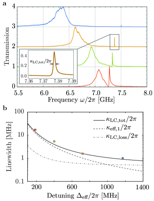
We determine the model parameters , by measuring the device in a cryostat at 4 K, where the niobium thin film of the LC resonator is superconducting. Microwave cavity transmission is measured for four different hats and the resulting power spectra are plotted in Fig. 3a. By fitting these curves to the theoretical transfer function, we extract the parameter averages and . Note that agrees well with the simulated coupling of 60 MHz between cavity and LC.
We next establish that Eq. (1) accurately models the device’s behavior. Fig. 3b shows the LC linewidths that are extracted directly from the measured transmission spectra. These are compared to a plot of the theoretical total loss rate that is obtained from Eq. (1) using the fitted model parameters. We observe that both agree well in the regime of large detuning. This allows us to infer the desirable and undesirable LC loss, which are plotted as and in the figure. Note that the wireless coupling has been varied by over an order of magnitude by using the different hats. In the target regime of 1.5-2.0 MHz for the effective coupling, the unwanted dissipation rate constitutes at most 30 % of the total LC loss rate. In a separate measurement, we find that the dissipation contribution is reduced to 17 % when operating the device in the millikelvin regime.
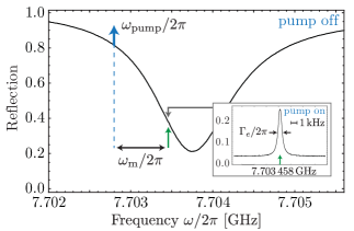
Finally, we demonstrate electromechanical interaction between the mechanical and LC resonators in the millikelvin environment of a dilution refrigerator. A coherent pump tone is applied at a frequency that is detuned from the LC resonator by approximately the mechanical frequency. The microwave cavity is then probed in reflection off the strongly coupled port. Fig. 4 shows the reflection spectrum with the pump tone turned off. The LC resonator appears as a dip, in contrast to a peak in transmission. In the presence of the pump tone, the interaction between the mechanical resonator’s motion and the photons stored in the LC circuit gives rise to a narrow peak on top of this feature. This phenomenon is commonly referred to as optomechanically induced transparency Weis et al. (2010); Teufel et al. (2011). For the LC circuit presented here, the pump tone leads to unexpected additional modes in the reflection spectrum. They likely are a result of weak glue joints between the silicon chips forming the microwave-to-optics transducer. In the Fig. 4 inset, we show the peak of an example mechanical mode at a frequency of 0.66 MHz. The electromechanical coupling rate of this mode to the LC resonator is lower than that of the desired 1.5 MHz mode. Therefore, a higher pump power has to be applied in order to observe the electromechanical interaction. This leads to a deeper LC resonance that is shifted down in frequency. With the pump turned on, the mechanics peak is centered on the shifted LC resonant frequency and displays a symmetric line shape. We have subsequently tested other chips that exhibit only the expected mode spectrum and the higher electromechanical coupling rate of the desired 1.5 MHz mode. For the transducer chip and pump tone chosen for this experiment, we demonstrate an electromechanical coupling strength of . This shows that the basic functionality of the electromechanical system is not altered by the additional microwave cavity.
In conclusion, we have overcome an important challenge of a microwave-to-optics converter design by placing the components inside a re-entrant microwave cavity. We were able to simplify the optical cavity assembly while achieving the desired performance of the microwave LC resonator. Going forward, we will test the full device including a functional optomechanical part. This device will be operated at mK temperatures in a dilution refrigerator, where we expect to enable microwave-to-optics conversion in the quantum regime. This constitutes an important step towards a quantum microwave-optics transducer that can readibly be integrated with other components of quantum information networks.
This work was supported by the AFOSR MURI under grant number FA9550-15-1-0015, and the National Science Foundation under grant number 1125844.
References
- Wallquist et al. (2009) M. Wallquist, K. Hammerer, P. Rabl, M. Lukin, and P. Zoller, Phys. Scr. T137 (2009).
- Barends et al. (2014) R. Barends, J. Kelly, A. Megrant, A. Veitia, D. Sank, E. Jeffrey, T. C. White, J. Mutus, A. G. Fowler, B. Campbell, Y. Chen, Z. Chen, B. Chiaro, A. Dunsworth, C. Neill, P. O’Malley, P. Roushan, A. Vainsencher, J. Wenner, A. N. Korotkov, A. N. Cleland, and J. M. Martinis, Nature 508, 500 (2014).
- Leghtas et al. (2015) Z. Leghtas, S. Touzard, I. M. Pop, A. Kou, B. Vlastakis, A. Petrenko, K. M. Sliwa, A. Narla, S. Shankar, M. J. Hatridge, M. Reagor, L. Frunzio, R. J. Schoelkopf, M. Mirrahimi, and M. H. Devoret, Science 347, 853 (2015).
- Reagor et al. (2016) M. Reagor, W. Pfaff, C. Axline, R. W. Heeres, N. Ofek, K. Sliwa, E. Holland, C. Wang, J. Blumoff, K. Chou, M. J. Hatridge, L. Frunzio, M. H. Devoret, L. Jiang, and R. J. Schoelkopf, Phys. Rev. B 94, 1 (2016).
- Ma et al. (2012) X.-S. Ma, T. Herbst, T. Scheidl, D. Wang, S. Kropatschek, W. Naylor, B. Wittmann, A. Mech, J. Kofler, E. Anisimova, V. Makarov, T. Jennewein, R. Ursin, and A. Zeilinger, Nature 489, 269 (2012).
- Tsang (2010) M. Tsang, Phys. Rev. A 81, 1 (2010).
- Safavi-Naeini and Painter (2011) A. H. Safavi-Naeini and O. Painter, New J. Phys. 13 (2011).
- Regal and Lehnert (2011) C. A. Regal and K. W. Lehnert, J. Phys. Conf. Ser. 264, 1 (2011).
- Axline et al. (2016) C. Axline, M. Reagor, R. Heeres, P. Reinhold, C. Wang, K. Shain, W. Pfaff, Y. Chu, L. Frunzio, and R. J. Schoelkopf, Appl. Phys. Lett. 109, 042601 (2016).
- Paik et al. (2011) H. Paik, D. I. Schuster, L. S. Bishop, G. Kirchmair, G. Catelani, a. P. Sears, B. R. Johnson, M. J. Reagor, L. Frunzio, L. I. Glazman, S. M. Girvin, M. H. Devoret, and R. J. Schoelkopf, Phys. Rev. Lett. 107, 1 (2011), arXiv:1105.4652 .
- Rigetti et al. (2012) C. Rigetti, J. M. Gambetta, S. Poletto, B. L. T. Plourde, J. M. Chow, A. D. Córcoles, J. A. Smolin, S. T. Merkel, J. R. Rozen, G. A. Keefe, M. B. Rothwell, M. B. Ketchen, and M. Steffen, Phys. Rev. B 86, 1 (2012).
- Narla et al. (2014) A. Narla, K. M. Sliwa, M. Hatridge, S. Shankar, L. Frunzio, R. J. Schoelkopf, and M. H. Devoret, Appl. Phys. Lett. 104, 232605 (2014).
- Yuan et al. (2015) M. Yuan, V. Singh, Y. M. Blanter, and G. A. Steele, Nat. Commun. 6, 8491 (2015).
- Noguchi et al. (2016) A. Noguchi, R. Yamazaki, M. Ataka, H. Fujita, Y. Tabuchi, T. Ishikawa, K. Usami, and Y. Nakamura, New J. Phys. 18 (2016).
- Andrews et al. (2014) R. W. Andrews, R. W. Peterson, T. P. Purdy, K. Cicak, R. W. Simmonds, C. A. Regal, and K. W. Lehnert, Nat. Phys. 10, 321 (2014).
- Peterson et al. (2016) R. W. Peterson, T. P. Purdy, N. S. Kampel, R. W. Andrews, P.-L. Yu, K. W. Lehnert, and C. A. Regal, Phys. Rev. Lett. 116, 063601 (2016).
- Aspelmeyer, Kippenberg, and Marquardt (2014) M. Aspelmeyer, T. J. Kippenberg, and F. Marquardt, Rev. Mod. Phys. 86, 1391 (2014).
- Purdy et al. (2012) T. P. Purdy, R. W. Peterson, P. L. Yu, and C. A. Regal, New J. Phys. 14 (2012).
- Note (1) The electromagnetic structure solver Ansys HFSS 15.0 is used.
- Weis et al. (2010) S. Weis, R. Rivière, S. Deléglise, E. Gavartin, O. Arcizet, A. Schliesser, and T. J. Kippenberg, Science 330, 1520 (2010).
- Teufel et al. (2011) J. D. Teufel, D. Li, M. S. Allman, K. Cicak, A. J. Sirois, J. D. Whittaker, and R. W. Simmonds, Nature 471, 204 (2011).