Potential 2D thermoelectric materials ATeI (A=Sb and Bi) monolayers from a first-principles study
Abstract
Lots of two-dimensional (2D) materials have been predicted theoretically, and further confirmed in experiment, which have wide applications in nanoscale electronic, optoelectronic and thermoelectric devices. Here, the thermoelectric properties of ATeI (A=Sb and Bi) monolayers are systematically investigated, based on semiclassical Boltzmann transport theory. It is found that spin-orbit coupling (SOC) has important effects on electronic transport coefficients in p-type doping, but neglectful influences on n-type ones. The room-temperature sheet thermal conductance is 14.2 for SbTeI and 12.6 for BiTeI, which are lower than one of most well-known 2D materials, such as transition-metal dichalcogenide, group IV-VI, group-VA and group-IV monolayers. By analyzing group velocities and phonon lifetimes, the very low sheet thermal conductance of ATeI (A=Sb and Bi) monolayers is mainly due to small group velocities. It is found that the high-frequency optical branches contribute significantly to the total thermal conductivity, being obviously different from usual picture with little contribution from optical branches. According to cumulative lattice thermal conductivity with respect to phonon mean free path (MFP), it is difficulty to further reduce lattice thermal conductivity by nanostructures. Finally, possible thermoelectric figure of merit of ATeI (A=Sb and Bi) monolayers are calculated. It is found that the p-type doping has more excellent thermoelectric properties than n-type doping, and at room temperature, the peak can reach 1.11 for SbTeI and 0.87 for BiTeI, respectively. These results make us believe that ATeI (A=Sb and Bi) monolayers may be potential 2D thermoelectric materials, and can stimulate further experimental works to synthesize these monolayers.
pacs:
72.15.Jf, 71.20.-b, 71.70.Ej, 79.10.-n Email:guosd@cumt.edu.cnI Introduction
Due to their potential applications in energy-related issues, thermoelectric materials have been widely investigated both in experiment and theoryq0 ; q1 . The performance of a thermoelectric material is measured by the dimensionless figure of merit , defined as , in which S, , T, and are the Seebeck coefficient, electrical conductivity, working temperature, the electronic and lattice thermal conductivities, respectively. To attain a high value, a high power factor () and/or a low thermal conductivity () are required. Unfortunately, these transport coefficients of bulk materials are coupled with each other, which are oppositely proportional to carrier density. Therefore, searching for high-performance thermoelectric materials is challenging.
The values of thermoelectric materials can be significantly enhanced by using low-dimensional systems or nanostructures, which is firstly proposed by Hicks and Dresselhaus in 1993q2 ; q3 . A large number of subsequent works have been centered on nanostructured materialsq4 ; q5 ; q6 , questing for highly efficient thermoelectric materials. Lots of 2D monolayers have been predicted in theory, or have been synthesized experimentally, including semiconducting transition-metal dichalcogenideq7 (such as and ), group IV-VIq8 (such as SnS and SnSe), group-VAq9 ; q10 (such as arsenene and antimonene) and group-IVq11 (such as germanene and stanene) monolayers. To design high-performance thermoelectric devices, the thermoelectric properties related with these 2D materials have also been investigated.
Based on ab-initio method and ballistic transport model,the thermoelectric properties of (M=Mo, W; X=S, Se) monolayers have been studiedq12 , and a maximum of monolayer is up to 0.5 at room temperature. For monolayer , a value of S as 30 mV/K has been reported experimentllyq13 . It has been proved that strain is a very effective strategy to improve thermoelectric properties of monolayer by enhancing power factor and reducing lattice thermal conductivityq14 . The transport coefficients of orthorhombic group IV-VI monolayers (A=Ge and Sn; B=S and Se) have been systematically investigated theoreticallyq15 ; q16 . The lattice thermal conductivities of - and -As, Sb monolayers have been performed in theoryq17 ; q18 ; q19 ; q20 . The thermoelectric properties of -As monolayer have been investigated with Green’s function based transport techniques21 , and thermoelectric properties of -Bi monolayer have also been studied by equilibrium molecular dynamics simulationsq22 . Phonon transport properties of group-IV monolayers (graphene, silicene, germanene and stanene) have been systematically investigated from ab initio calculationsq23 , and it is found that the lattice thermal conductivity for graphene, silicene and germanene decreases monotonically, but higher lattice thermal conductivity is observed in stanene.
Recently, based on the first-principles calculations, stable ATeI (A=Sb and Bi) monolayers have been predicted with a giant Rashba spin splittingq24 ; q25 . The thermoelectric properties related with bulk BiTeI have been performedq26 , and the figure of merit at 300 K is 0.05, and the of undoped BiTeI reaches 0.3 at 520 K. The thermoelectric performance of bulk BiTeI can be improved in Cu-intercalated BiTeI q27 or through Br-substitutionq28 . The pressure-enhanced power factor has been predicted by the first-principles calculations in bulk BiTeIq29 . Here, we systematically study the thermoelectric performance of ATeI (A=Sb and Bi) monolayers by combining the first-principles calculations and semiclassical Boltzmann transport theory. It is necessary for calculations of electronic transport coefficients of ATeI (A=Sb and Bi) monolayers to include SOC. The calculated sheet thermal conductances of ATeI (A=Sb and Bi) monolayers are lower than ones of other well-studied 2D materials. The contribution to total thermal conductivity from high-frequency optical branches is larger than 19%. This is different from the usual picture that high frequency optical branches have very little contribution. Based on calculated , ATeI (A=Sb and Bi) monolayers may be potential 2D thermoelectric materials.
The rest of the paper is organized as follows. In the next section, we shall give our computational details about calculations of electronic structures, electron and phonon transport. In the third section, we shall present electronic structures, electron and phonon transport of ATeI (A=Sb and Bi) monolayers. Finally, we shall give our discussions and conclusions in the fourth section.
II Computational detail
A full-potential linearized augmented-plane-waves method within the density functional theory (DFT) 1 is employed to carry out electronic structures of ATeI (A=Sb and Bi) monolayers, as implemented in the WIEN2k code 2 . The GGA of Perdew, Burke and Ernzerhof (GGA-PBE)pbe is used to optimize free atomic position parameters with a force standard of 2 mRy/a.u.. The SOC is included self-consistently 10 ; 11 ; 12 ; so due to large Rashba spin splitting, which produces important effects on electronic transport coefficients. The convergence results are determined by using 4000 k-points in the first Brillouin zone (BZ) for the self-consistent calculation, making harmonic expansion up to in each of the atomic spheres, and setting for the plane-wave cut-off. The self-consistent calculations are considered to be converged when the integration of the absolute charge-density difference between the input and output electron density is less than per formula unit, where is the electron charge.
Based on calculated energy band structures, transport coefficients of electron part, including Seebeck coefficient and electrical conductivity, are calculated through solving Boltzmann transport equations within the constant scattering time approximation (CSTA), as implemented in BoltzTrap codeb , which shows reliable results in many classic thermoelectric materialsb1-1 ; b2 ; b3 . To obtain accurate transport coefficients, the parameter LPFAC is set as 20, and at least 2000 k-points is used in the irreducible BZ for the calculation of energy band structures. The lattice thermal conductivities are performed by using Phono3py+VASP codespv1 ; pv2 ; pv3 ; pv4 . The second order harmonic and third order anharmonic interatomic force constants (IFC) are calculated by using a 5 5 1 supercell and a 3 3 1 supercell, respectively. To compute lattice thermal conductivities, the reciprocal spaces of the primitive cells are sampled using the 40 40 2 meshes.
For 2D material, the calculated electrical conductivity, electronic and lattice thermal conductivities depend on the length of unit cell along z direction2dl . They should be normalized by multiplying Lz/d, where Lz is the length of unit cell used in the calculations along z direction and d is the thickness of 2D material, but the d is not well defined. However, the dimensionless figure of merit is independent of the length of unit cell along z direction. In this work, the length of unit cell (20 ) along z direction is used as the thickness of ATeI (A=Sb and Bi) monolayers. By d, the thermal sheet conductance can be attained, which is used to compare the thermal conductivities of various 2D monolayers.
| Name | - | ||||
|---|---|---|---|---|---|
| SbTeI | 4.32 | 1.17 | 0.90 | 0.27 | 18 |
| BiTeI | 4.42 | 1.52 | 0.69 | 0.83 | 42 |

III MAIN CALCULATED RESULTS AND ANALYSIS
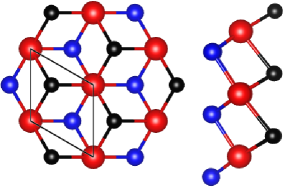
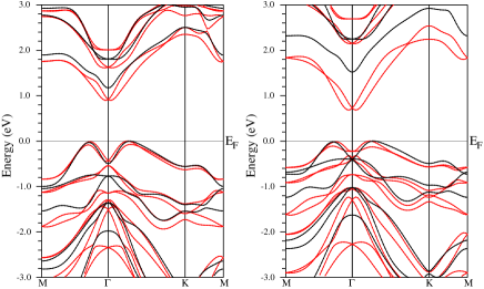
ATeI (A=Sb, I) monolayers can be attained from their bulk counterparts with a trigonal structure, and they consist of three sublayers with A atoms in the center sublayer, while Te and I atoms are located in the top and bottom sublayers. The schematic crystal structure is plotted in Figure 1. The unit cell of ATeI (A=Sb, I) monolayers, containing one A, one Te and one I atoms, is built with the vacuum region of larger than 15 to avoid spurious interaction. The optimized lattice constantsq25 within GGA-PBE are used to investigate their electronic structures and thermoelectric properties, and free atomic positions are also optimized. Figure 2 shows the energy band structures of ATeI (A=Sb, I) monolayers using both GGA and GGA+SOC. At the absence of SOC, ATeI (A=Sb, I) monolayers are both semiconductors with the conduction band minimum (CBM) at the point, and with two valence band maxima (VBM) between the and K or M points. When the SOC is considered, two CBM are located slightly shifted away from point along the -K and -M paths due to Rashba effect, and the energy band gap is reduced from 1.17 eV to 0.90 eV for SbTeI, and from 1.52 eV to 0.69 eV for BiTeI. The Rashba energy of ATeI (A=Sb, I) monolayers, defined as the energy difference between the CBM and the band crossing point of conduction bands at point, is 18 meV and 42 meV, respectively. Some key data are shown in Table 1, which agree well with previous resultsq25 .
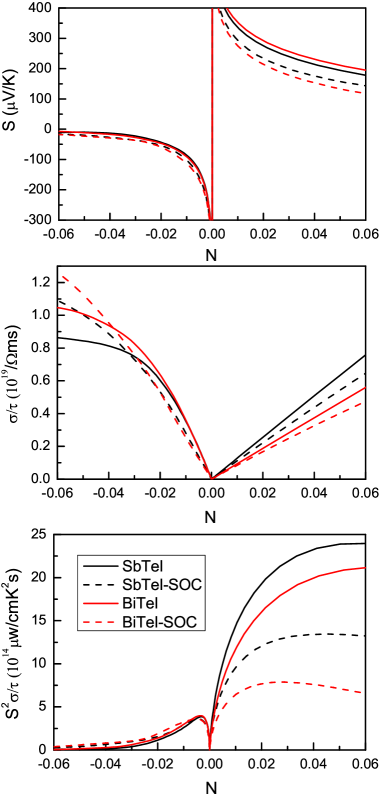
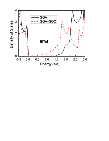
Based on calculated energy band structures, the electronic transport coefficients of ATeI (A=Sb, I) monolayers can be attained using CSTA Boltzmann theory. The calculated Seebeck coefficient is independent of scattering time, while electrical conductivity depends on scattering time. Figure 3 shows the Seebeck coefficient S, electrical conductivity with respect to scattering time and power factor with respect to scattering time as a function of doping level using both GGA and GGA+SOC at room temperature. By simply shifting Fermi level into conduction or valence bands, the n- or p-type doping level can be simulated within the framework of rigid band approach. The approximation is effective in low doping levelq30 ; q31 ; q32 . It is found that SOC has a slightly enhanced effect on n-type Seebeck coefficient, but has a obviously reduced influence on p-type Seebeck coefficient. According to Figure 4, the slope of density of states (DOS) of valence bands of BiTeI near the energy band gap with GGA+SOC decreases with respect to one with GGA, which leads to reduced S. Similar results can be found in SbTeI. For , the detrimental influence caused by SOC can be observed in p-type and low n-type doping. A signally reduced effect on p-type power factor can be caused by SOC, while a neglectful influence on n-type power factor can be observed.
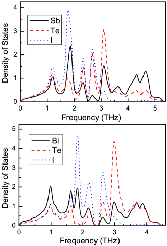
Based on calculated harmonic IFCs, the phonon dispersions of ATeI (A=Sb, I) monolayers, determining the group velocities and allowed three phonon scattering processes, are attained along high-symmetry pathes, which are plotted in Figure 5, together with partial DOS in Figure 6. The 3 acoustic and 6 optical phonon branches in the phonon spectra can be observed due to three atoms in the unit cell of ATeI (A=Sb, I) monolayers. It is clearly seen that the longitudinal acoustic (LA) and transverse acoustic (TA) branches are linear near the point, while the z-direction acoustic (ZA) branch is quadratic. Similar results can be found in many other 2D materialsq15 ; q17 ; q18 ; q19 ; q23 . The whole phonon branches move toward lower energy from SbTeI to BiTeI monolayer, which suggests the phonon dispersion becomes more localized. The width of acoustic branches is 1.80 THz and 1.71 THz from SbTeI to BiTeI monolayer, which is also maximal acoustic vibration frequency (MAVF). The low MAVF means small group velocities, producing low lattice thermal conductivity. It is a very noteworthy phenomenon that the last two optical branches have very large dispersions, which may lead to obvious contribution to lattice thermal conductivity. According to Figure 6, the high-frequency optical modes of ATeI (A=Sb, I) monolayers are mainly from A and Te vibrations, while the low-frequency optical and acoustic branches are due to the vibrations of all atoms.
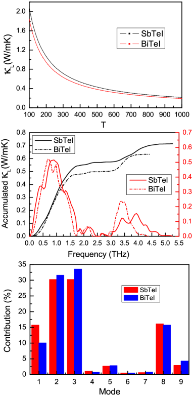
The lattice thermal conductivities of ATeI (A=Sb, I) monolayers as a function of temperature and the accumulated lattice thermal conductivity (300 K) along with the derivatives are plotted in Figure 7. The room-temperature lattice thermal conductivity of ATeI (A=Sb, I) monolayers is 0.71 and 0.63 with the same thickness 20 , respectively. To compare their thermal conductivities with ones of other 2D materials, the room-temperature thermal conductivity is converted into thermal sheet conductance2dl , and the corresponding value is 14.2 and 12.6 , respectively. Their thermal sheet conductances are lower than one of semiconducting transition-metal dichalcogenide, group IV-VI, group-VA and group-IV (expect germanene) monolayersq23 ; 2dl ; q33 . The very low thermal sheet conductance suggests that SbTeI and BiTeI monolayers are potential 2D thermoelectric materials. The cumulative lattice thermal conductivity and the derivatives show that the acoustic phonon branches dominate lattice thermal conductivity, and the high-frequency optical modes have obvious contribution to lattice thermal conductivity. The acoustic branches comprise around 76.13% for SbTeI and 75.10% for BiTeI, respectively. Furthermore, the relative contributions of nine phonon modes to the total lattice thermal conductivity at 300K are plotted in Figure 7. It is found that ZA branch provides the smallest contribution in acoustic branches, while the LA and TA branches have about the same contribution. It is a surprising thing that the last two optical branches of SbTeI and BiTeI monolayers provide a contribution of 19.02% and 20.03%, which is different from usual picture with little contribution from optical branches. Moreover, the second optical branch has also relatively large contribution to the total lattice thermal conductivity.
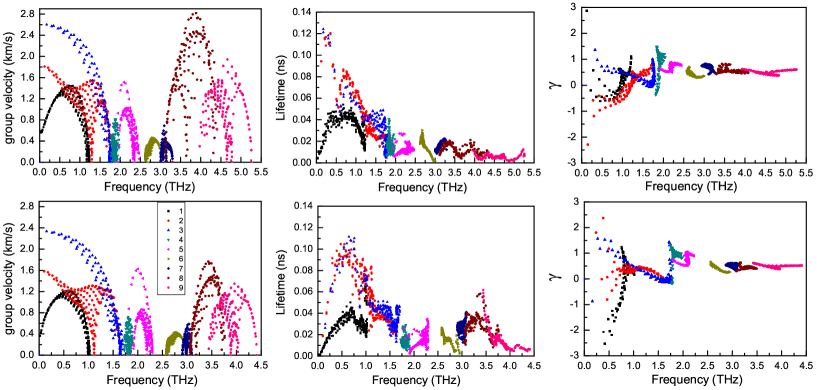
According to Figure 8, the group velocities of LA and TA branches are larger than ones of ZA branch, due to quadratic dispersion of ZA branch near the point. The largest group velocity for ZA, TA and LA branches near point is 0.58 , 1.81 and 2.60 for SbTeI monolayer and 0.36 , 1.58 and 2.34 for BiTeI monolayer. In other 2D materials, larger phonon group velocities near point can be found than in ATeI (A=Sb, I) monolayers, such as in blue phosphorene, arsenene, antimonene, stanene and siliceneq15 ; q17 ; q18 ; q19 ; q23 . The small phonon group velocities can lead to lower thermal conductivity in ATeI (A=Sb, I) monolayers than in other 2D materials. The group velocities become smaller from SbTeI to BiTeI monolayer, and then a decrescent lattice thermal conductivity can be induced. It is very rare that optical modes have very large group velocities, especially for the second and last two optical branches. For SbTeI, the maximum group velocity of the fifth optical branch is 2.82 , which is larger than maximum group velocity of acoustic branches. These suggest that optical branches play an important role in determining lattice thermal conductivity of ATeI (A=Sb, I) monolayers.
Phonon lifetimes of ATeI (A=Sb, I) monolayers at room temperature are also plotted in Figure 8, which can attained by the phonon linewidth. In the single-mode relaxation time methodpv4 , the phonon lifetimes and lattice thermal conductivity are merely proportional to each other. The most lifetimes of ZA branch is shorter than ones of LA and TA branches, which leads to smaller contribution to lattice thermal conductivity for ZA branch than LA and TA branches. The lifetimes of most acoustic modes of SbTeI are between 20 ps and 80 ps, and 20 ps and 100 ps for BiTeI. The lifetimes of most optical modes are less than 20 ps for SbTeI, but ones of high-frequency optical modes of BiTeI are well-matched with ones of ZA branches. By considering group velocities and phonon lifetimes, smaller group velocities for BiTeI than SbTeI lead to lower lattice thermal conductivity. Based on third order anharmonic IFCs, mode Grneisen parameters can be attained, which is shown in Figure 8. Most of they are positive, especially for optical branches. The mode Grneisen parameters can be used to describe the anharmonicity of materials, and larger can lead to lower lattice thermal conductivity because of strong anharmonic phonon scattering. It is found that Grneisen parameters of ZA branch of BiTeI are larger than of ones of SbTeI, which induces lower intrinsic thermal conductivity for BiTeI than SbTeI.
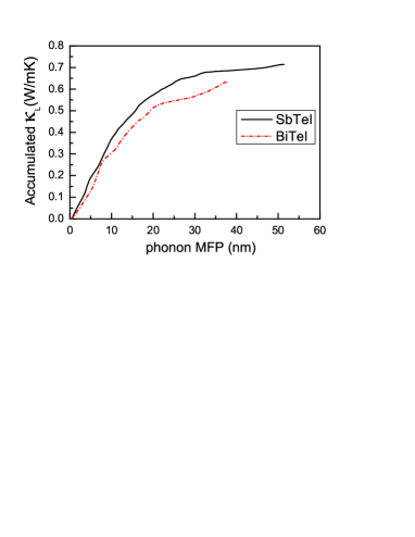
To quantify the contribution from phonons with various mean free paths (MFP), the cumulative lattice thermal conductivity with respect to phonon MFP is plotted in Figure 9 at room temperature. The cumulative lattice thermal conductivity increases with MFP increasing, and then approaches maximum after MFP reaches 51.4 nm for SbTeI and 37.7 nm for BiTeI, respectively. When the characteristic length is smaller than 51.4 nm for SbTeI and 37.7 nm for BiTeI, the lattice thermal conductivity can be significantly reduced. The stronger intrinsic phonon scattering, causing phonons to have shorter MFP, can induce lower lattice thermal conductivity. These critical values are very small, so scale reduction may be difficult to reduce lattice thermal conductivity.
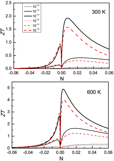
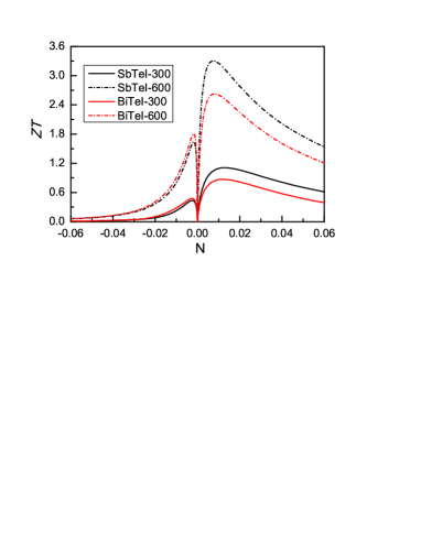
To estimate the efficiency of thermoelectric conversion, the figure of merit is calculated, based on calculated electron and phonon transport coefficients. However, scattering time is unknown, which can be attained by comparing experimental value of electronic conductivity with the calculated value . Firstly, some empirical values, such as 1 s, 1 s and 1 s, are used to calculate the power factor and electronic thermal conductivity. Here, the electrical thermal conductivities are calculated by the Wiedemann-Franz law with the Lorenz number of 2.4 , which is also used in bulk BiTeIq26 . At 300 and 600 K, the possible of ATeI (A=Sb, I) monolayers with respect to doping level are shown in Figure 10. The =, where , which is independent of , as an upper limit of . The increasing makes be more close to one, which leads to increasing with changing from 1 s to 1 s. It is found that the p-type doping for ATeI (A=Sb, I) monolayers shows more excellent than n-type doping. Calculated results show that SbTeI monolayer has better thermoelectric properties than BiTeI monolayer in p-type doping due to larger , while they show almost equivalent in n-type doping. In p-type doping, a peak is up to 1.65 for SbTeI and 1.23 for BiTeI using classic = s at 600 K. For bulk BiTeI, the related experimental transport coefficients can be found in ref.q34 . Finally, the is calculated by comparing experimental values of the n-type conductivity of bulk BiTeI with the calculated values of q29 at room temperature. The scattering time is found to be 3.93 s, which is also used in ATeI (A=Sb, I) monolayers. The recomputed of ATeI (A=Sb, I) monolayers as a function of doping level with being 3.93 s are plotted in Figure 11. At room temperature, the peak reaches 1.11 for SbTeI and 0.87 for BiTeI, respectively.
| GeS | GeSe | SnS | SnSe | ||||
|---|---|---|---|---|---|---|---|
| 52.93 | 31.58 | 18.68 | 17.55 | 77.89 | 62.14 | 97.35 | 69.38 |
| Si | Ge | Sn | As | Sb | Bi | SbTeI | BiTeI |
| 120.12 | 11.39 | 26.04 | 161.10 | 46.62 | 16.02 | 14.20 | 12.60 |
IV Discussions and Conclusion
ATeI (A=Sb, I) monolayers display the Rashba effect due strong SOC, which significantly changes their conduction and valence bands. However, SOC has little effect on n-type Seebeck coefficient, leading to little influence on n-type power factor. For bulk BiTeI, a detrimental influence on n-type Seebeck coefficient can be observedq29 . For BiTeI monolayer, the SOC not only can remove the degeneracy of conduction bands, but also can make conduction bands to be more localized. The two combined factors lead to little influence on n-type Seebeck coefficient caused by SOC. For both bulk and monolayer BiTeI, the reduced effect on p-type Seebeck coefficient can be produced by SOC.
Low lattice thermal conductivity is very crucial for potential thermoelectric materials. To make a fair comparison for thermal transport capability of 2D materials, the same thickness should be used, or the sheet thermal conductance should be adopted2dl . The sheet thermal conductances of ATeI (A=Sb, I) monolayers, some semiconducting transition-metal dichalcogenide, group IV-VI, group-VA and group-IV monolayersq23 ; 2dl ; q33 are summarized in Table 2. The sheet thermal conductances of ATeI (A=Sb, I) monolayers are lower than that of semiconducting transition-metal dichalcogenide, group IV-VI, group-VA and group-IV monolayers except Ge monolayer, which suggests that they may be potential 2D thermoelectric material compared to other well-known 2D materials. It is found that the small phonon group velocities lead to low sheet thermal conductances of ATeI (A=Sb, I) monolayers.
In summary, we have employed first-principles calculations and semiclassical Boltzmann transport theory to investigate the thermoelectric properties of ATeI (A=Sb, I) monolayers. It is found that SOC can produce important effects on electronic structures and transport coefficients due to Rashba effect in ATeI (A=Sb, I) monolayers. The sheet thermal conductance is employed to make a fair comparison for lattice thermal conductivities of different 2D materials. The sheet thermal conductances of ATeI (A=Sb, I) monolayers are lower than one of other well-studied 2D materials due to small group velocities. It is found that the high-frequency optical branches make a considerable contribution to the total lattice thermal conductivity. Nanostructuring is difficult to further reduce the lattice thermal conductivity unless their characteristic lengths are less than 51.4 nm for SbTeI and 37.7 nm for BiTeI. According to estimated , ATeI (A=Sb, I) monolayers may be potential 2D thermoelectric materials, which can stimulate further experimental works to synthesize these 2D monolayers.
Acknowledgements.
This work is supported by the National Natural Science Foundation of China (Grant No. 11404391). We are grateful to the Advanced Analysis and Computation Center of CUMT for the award of CPU hours to accomplish this work.References
- (1) T. M. Tritt and M. A. Subramanian, MRS Bulletin 31, 188 (2006).
- (2) G. J. Snyder and E. S. Toberer, Nature Materials 7, 105 (2008).
- (3) L. D. Hicks and M. S. Dresselhaus, Phys. Rev. B 47, 12727 (1993).
- (4) L. D. Hicks and M. S. Dresselhaus, Phys. Rev. B 47, 16631(R) (1993).
- (5) A. J. Minnich, M. S. Dresselhaus, Z. F. Ren and G. Chen, Energy Environ. Sci. 2, 466 (2009).
- (6) A. I. Boukai, Y. Bunimovich, J. T. Kheli, J. K. Yu, W. A. Goddard III and J. R. Heath, Nature 451, 168 (2008).
- (7) T. C. Harman, P. J. Taylor, M. P. Walsh and B. E. LaForge, Science 297, 2229 (2002).
- (8) M. Chhowalla, H. S. Shin, G. Eda, L. J. Li, K. P. Loh and H. Zhang, Nature Chemistry 5, 263 (2013).
- (9) R. X. Fei, W. B. Li, J. Li and L. Yang, Appl. Phys. Lett. 107, 173104 (2015).
- (10) S. L. Zhang et al., Angew. Chem. 128, 1698 (2016).
- (11) J. P. Ji et al., Nat. Commun. 7, 13352 (2016).
- (12) S. Balendhran, S. Walia, H. Nili, S. Sriram and M.Bhaskaran, small 11, 640 (2015).
- (13) W. Huang, H. X. Da and G. C. Liang, J. Appl. Phys. 113, 104304 (2013).
- (14) J. Wu et al. Nano Lett. 14, 2730 (2014).
- (15) S. D. Guo, J. Mater. Chem. C 4, 9366 (2016).
- (16) G. Qin, Z. Qin, W. Fang, L. Zhang, S. Yue, Q. Yan, M. Hu and G. Su, Nanoscale 8, 11306 (2016).
- (17) S. D. Guo and Y. H. Wang, J. Appl. Phys. 121, 034302 (2017).
- (18) S. D. Wang, W. H. Wang and G. J. Zhao, Phys. Chem. Chem. Phys. 18, 31217 (2016).
- (19) G. H. Zheng, Y. L. Jia, S. Gao and S. H. Ke, Phys. Rev. B 94, 155448 (2016).
- (20) M. Zeraati, S. M. V. Allaei, I. A. Sarsari, M. Pourfath, and D. Donadio, Phys. Rev. B 93, 085424 (2016).
- (21) T. Zhang, Y. Y. Qi, X. R. Chen and L. C. Cai, Phys. Chem. Chem. Phys. 18, 30061 (2016).
- (22) L. M. Sandonas,D. Teich, R. Gutierrez, T. Lorenz, A. Pecchia, G. Seifert and G. Cuniberti, J. Phys. Chem. C 120, 18841 (2016).
- (23) L. Cheng, H. J. Liu, X. J. Tan, J. Zhang, J. Wei, H. Y. Lv, J. Shi and X. F. Tang, J. Phys. Chem. C 118, 904 (2014).
- (24) B. Peng, H. Zhang, H. Z. Shao, Y. F. Xu, G. Ni, R. J. Zhang and H. Y. Zhu, Phys. Rev. B 94, 245420 (2016).
- (25) Y. D. Ma, Y. Dai, W. Wei, X. R. Li and B. B. Huang, Phys. Chem. Chem. Phys. 16, 17603 (2014).
- (26) H. L. Zhuang, V. R. Cooper, H. Y. Xu, P. Ganesh, R. G. Hennig and P. R. C. Kent, Phys. Rev. B 92, 115302 (2015).
- (27) L. H. Wu, J. Yang, S. Y. Wang, P. Wei, J. H. Yang, W. Q. Zhang and L. D. Chen, Phys. Rev. B 90, 195210 (2014).
- (28) L. H. Wu, J. Yang, M. F. Chi, S. Y. Wang, P. Wei, W. Q. Zhang, L. D. Chen and J. H. Yang, Sci. Rep. 5, 14319 (2015).
- (29) L. H. Wu, J. Yang, T. S. Zhang, S. Y. Wang, P. Wei, W. Q. Zhang, L. D. Chen and J. H. Yang, J. Phys.: Condens. Matter 28, 085801 (2016).
- (30) S. D. Guo and J. L. Wang, J. Phys. D: Appl. Phys. 49, 215107 (2016).
- (31) P. Hohenberg and W. Kohn, Phys. Rev. 136, B864 (1964); W. Kohn and L. J. Sham, Phys. Rev. 140, A1133 (1965).
- (32) P. Blaha, K. Schwarz, G. K. H. Madsen, D. Kvasnicka and J. Luitz, WIEN2k, an Augmented Plane Wave + Local Orbitals Program for Calculating Crystal Properties (Karlheinz Schwarz Technische Universität Wien, Austria) 2001, ISBN 3-9501031-1-2
- (33) J. P. Perdew, K. Burke and M. Ernzerhof, Phys. Rev. Lett. 77, 3865 (1996).
- (34) A. H. MacDonald, W. E. Pickett and D. D. Koelling, J. Phys. C 13, 2675 (1980).
- (35) D. J. Singh and L. Nordstrom, Plane Waves, Pseudopotentials and the LAPW Method, 2nd Edition (Springer, New York, 2006).
- (36) J. Kunes, P. Novak, R. Schmid, P. Blaha and K. Schwarz, Phys. Rev. B 64, 153102 (2001).
- (37) D. D. Koelling, B. N. Harmon, J. Phys. C Solid State Phys. 10, 3107 (1977).
- (38) G. K. H. Madsen and D. J. Singh, Comput. Phys. Commun. 175, 67 (2006).
- (39) B. L. Huang and M. Kaviany, Phys. Rev. B 77, 125209 (2008).
- (40) L. Q. Xu, Y. P. Zheng and J. C. Zheng, Phys. Rev. B 82, 195102 (2010).
- (41) J. J. Pulikkotil, D. J. Singh, S. Auluck, M. Saravanan, D. K. Misra, A. Dhar and R. C. Budhani, Phys. Rev. B 86, 155204 (2012).
- (42) G. Kresse, J. Non-Cryst. Solids 193, 222 (1995).
- (43) G. Kresse and J. Furthmller, Comput. Mater. Sci. 6, 15 (1996).
- (44) G. Kresse and D. Joubert, Phys. Rev. B 59, 1758 (1999).
- (45) A. Togo, L. Chaput and I. Tanaka, Phys. Rev. B 91, 094306 (2015).
- (46) X. F. Wu, V. Varshney et al., Chem. Phys. Lett. 669, 233 (2017).
- (47) T. J. Scheidemantel, C. Ambrosch-Draxl, T. Thonhauser, J. V. Badding and J. O. Sofo, Phys. Rev. B 68, 125210 (2003).
- (48) G. K. H. Madsen, J. Am. Chem. Soc. 128, 12140 (2006).
- (49) X. Gao, K. Uehara, D. Klug, S. Patchkovskii, J. Tse and T. Tritt, Phys. Rev. B 72, 125202 (2005).
- (50) D. C. Zhang, A. X. Zhang and S. D. Guo, arXiv:1701.08944 (2017).
- (51) V. A. Kulbachinskii, V. G.Kytin, A. A. Kudryashov, A. N. Kuznetsov and A. V. Shevelkov, J. Sold State Chem. 193, 154 (2012).