Polarized SERS of individual suspended carbon nanotubes by Pt-Re nanoantennas
Abstract
We present optical nanoantennas designed for applications that require processing temperatures larger than 800∘C. The antennas consist of arrays of Re/Pt bilayer strips fabricated with a lift-off-free technique on top of etched trenches. Reflectance measurements show a clear plasmonic resonance at approximately 670 nm for light polarized orthogonal to the strip axis. The functionality of the antennas is demonstrated by growing single-walled carbon nanotubes (CNTs) on top of the antenna arrays and measuring the corresponding Raman signal enhancement of individual CNTs. The results of the measurements are quantitatively discussed in light of numerical simulations which highlight the impact of the substrate.
pacs:
78.67.Ch, 78.30.-j, 63.22.Gh, 61.48.De, 52.40.Fd, 42.79.DjThe key feature of plasmonic nanostructures is their ability to confine light on a much smaller scale compared to the far field wavelength Novonty and Hecht (2006); Tame et al. (2013). As a consequence, such structures are able to amplify the optical near field at their surface by many orders of magnitude, especially if a localized surface plasmon resonance (LSPR) is excited. This has a dramatic impact on optical spectroscopy, where the near field amplification makes it possible to detect spectra of single molecules Kneipp et al. (1997); Nie (1997); Chikkaraddy et al. (2016). In particular, the use of plasmonic structures represented a fundamental breakthrough for Raman spectroscopy, where it is referred to as surface-enhanced Raman spectroscopy (SERS) Moskovits (1985); Stosch et al. (2011); Kneipp et al. (2004). The name reflects the fact that early experiments made use of granular metallic surfaces Moskovits (1985); Fleischmann et al. (1974); Creighton (1982). Subsequently, colloidal Au or Ag nanoparticles Creighton (1982); Benner et al. (1983); Weitz and Oliveria (1984), as well as periodically indented metal layers Sanda et al. (1980); Liao et al. (1981) were used as plasmonic resonators. Such resonators act as optical nanoantennas, i.e. they concentrate propagating radiation into a subwavelength-sized region where the near field dominates the far field.
The progress of nanoplasmonics enabled the fabrication of optical nanoantennas specifically designed to work in combination with given target molecules Kneipp et al. (1997); Nie (1997). The combination of plasmonic structures with specific devices has nevertheless a limit: the fabrication of the target device or the synthesis of the desired molecule is not always compatible with the fabrication of the optical nanoantennas. Carbon nanotubes (CNTs) represent a good example of such a situation. The fabrication of ultra-clean devices [IntheliteratureCNTswhichhaveneverbeensubjectedtoanyfabricationstepandarenotinteractingwiththesubstratearecalledultra-cleanCNTs]SMNote2 often requires that the CNT growth must be performed as last fabrication step Cao et al. (2005); Laird et al. (2015). CNTs are grown by chemical vapor deposition (CVD) at temperatures of the order of 800∘C or higher Saito et al. (1998). These temperatures are sufficient to melt thin films or nanoparticles of the most common plasmonic materials, namely Au and Ag. Therefore so far the proposed prototypes Kneipp et al. (2000); Chu et al. (2009); Heeg et al. (2014); Paradiso et al. (2015) of optical nanoantennas for CNTs had to be fabricated or deposited after the CNT growth, i.e. they were not compatible with the ultra-clean fabrication scheme.
The low degree of disorder in ultra-clean CNTs allows for a detailed comparison of quantum transport experiments with microscopic theories Laird et al. (2015). For such analysis an independent determination of diameter and chiral angle is highly desirable Cao et al. (2004); Dirnaichner et al. (2016). Such information could in principle be provided by Raman spectroscopy, but only in the rare case that the energy of the incident or scattered photon energy matches the energy separation between two van Hove singularities (VHS) of the CNT density of states Kataura et al. (1999); Jorio et al. (2001); Maultzsch et al. (2005).
In experiments with CNTs grown on top of predefined electrodes one deals typically with few devices. Without the usage of tunable lasers it is unlikely to meet the Raman resonance condition for an individual contacted CNT. The field amplification induced by plasmonic structures can be crucial to obtain a sizable optical signal from a limited number of contacted devices.
In the present work we developed optical nanoantennas which are resistant to the extreme conditions of the nanotube CVD growth. We use spatially resolved reflectance measurements to demonstrate the occurrence of a localized surface plasmon resonance (LSPR) at around 630–670 nm. Finally, we exploit the induced field enhancement to magnify the Raman signal of individual ultra-clean CNTs.
I Experimental details
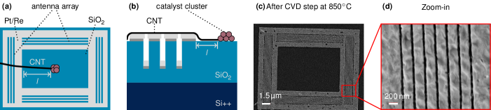
Our sample fabrication is sketched in Fig. 1. The antenna arrays are fabricated on degenerately doped silicon substrates with a 470 nm-thick SiO2 cap layer. The fabrication process starts with the etching of trenches defined by electron beam lithography (EBL). 30-nm-wide, 100-nm-deep and 6-m-long trenches are distributed in arrays of 9 elements with a periodicity of 240 nm. Four arrays are arranged as the four sides of a rectangle. On top of the trenches, we deposited a Re-Pt (with thickness 7 and 18 nm, respectively) metal bilayer. The choice of Re as sticking layer is motivated by its extraordinary stability at high temperatures. Even when reduced to a few-nanometer-thin layer, Re can stand temperatures as high as 900∘C with negligible structural deformation. On the other hand, at these temperatures Pt nanostructures suffer major roughening, while most metals (including common plasmonic materials as, e.g., Au, Ag, Pd, Al) simply melt. We found that the combination of Re as sticking layer and Pt as top layer is the best compromise between the thermal stability provided by Re, and the plasmonic performances and chemical stability guaranteed by Pt.
Etched trenches make possible to control the gap width between adjacent metal strips: the thicker the metal layer, the thinner is the residual gap Le Thi Ngoc et al. (2013). The metallization does not cover the entire sample surface, but it is limited to EBL-defined square frames overlapping the trenches, as shown in Fig. 1(a,c). In particular the inner part of the rectangular frame is not metallized: here a 1 m-wide cluster of catalyst nanoparticles is patterned by EBL [SeetheSupplementalMaterialforfurtherdetails]SMnote1.
The last fabrication step is the CVD growth. This step takes place at 850∘C under a steady stream of CH4 and H2. CNTs start growing vertically from the catalyst cluster. Owing to Van-der-Waals interaction, they bend downwards during the growth until they eventually fall on the substrate or on the antennas Huang et al. (2003). Most CNTs are shorter than the cluster-to-antenna distance m. However, some CNTs grow long enough to bridge the antennas. Owing to the small gap between the antenna strips, the CNTs are suspended over the substrate. The CNT position and orientation is clearly unpredictable, thus it is determined a posteriori by atomic force microscopy (AFM).
Beside the antenna structure described above we have investigated also alternative structures where the nanoantenna arrays are defined by EBL followed by metal deposition and lift-off, i.e. without making use of etched trenches. Each strip of the arrays consists a bilayer of 5 nm of Ti (sticking layer) and 20 nm of Pt. Although the final results are qualitatively similar, the use of etched trenches makes the fabrication process more reproducible and reliable. Moreover, etched trenches help to keep the gap between the strips homogeneous and avoid that the roughness caused by the CVD step could short-circuit adjacent strips.
Raman and reflectance measurements are performed in a confocal setup [SeetheSupplementalMaterialforfurtherdetails]SMnote1; Stosch et al. (2011); Paradiso et al. (2015). Light is transmitted through a beam splitter and focused on the sample by a objective lens. The light spot size is approximately m for white light and below m for the two laser lines, i.e. the spatial resolution is comparable to the array width. The scattered light is transmitted again through the beam splitter and then sent to the detector, as discussed in our previous work Paradiso et al. (2015). The configuration of light sources, detectors and polarizers depends on the specific measurement [SeetheSupplementalMaterialforfurtherdetails]SMnote1. For reflectance spectroscopy we use a thermal source of white light and a spectrometer as detector. An analyzer is placed in between the sample and the spectrometer. For reflectance maps the light source is a laser (either a He/Ne laser with nm or a diode laser with nm) and the detector is a power–meter. A polarizer is placed between the source and the sample. The same configuration is used for Raman spectroscopy. In this case the detector is a spectrometer.
II Experimental results
Long metal nanowires display a plasmonic resonance near the visible when excited with a field orthogonal to their axis, where the incompressible electron plasma experiences a non-negligible restoring force Novonty and Hecht (2006); Le Thi Ngoc et al. (2013). The excitation of a LSPR implies losses due to absorption in the metal, which results in a reduction of the scattered light intensity. If a metal nanowire is illuminated with white light polarized orthogonally to the wire axis, plasmonic resonances will appear therefore as minima in the spectrum of the reflected light. On the other hand, when an antenna array is excited with unpolarized light, only the polarization component perpendicular to the array axis will show a minimum at the LSPR, while the parallel component will be scarcely affected.
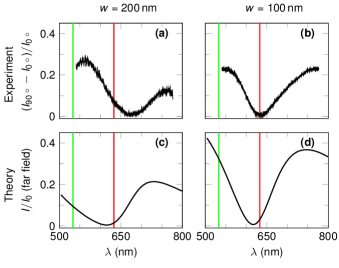
In our reflectance spectroscopy measurements we keep the analyzer oriented vertically [i.e. parallel to the shorter side of the rectangle in Fig. 1(c)] and we measure the reflected signal from two arrays, one oriented horizontally () and the other oriented vertically (), where the latter represents the background signal. The difference of the two signals is then normalized to the background signal () [Thesameresultcanbeobtainedbyrotatingtheanalyzeronthesamearray.Themethodheredescribedishowevermoreaccuratesincetheopticaltransmissionofoursetupisslightlypolarizationandwavelengthdependent]SMNote3. Figure 2(a,b) shows the difference between and , divided by the latter. The panel (a) refers to a Re/Pt antenna array patterned on etched trenches. The graph clearly displays a minimum in the reflected signal at nm, which is close to the laser wavelength nm used in our Raman experiments. The graph in Fig. 2(b) shows data obtained on a EBL-defined antenna array, i.e. without etched trenches. In this case the minimum occurs at a slightly lower wavelength, nm. Graphs in Fig. 2(c) and (d) show the corresponding results of the numerical simulations discussed in Sec. III.
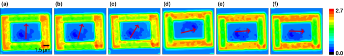
To confirm the resonant nature of the observed minimum, we acquired maps of the reflected signal as a function of the polarization of the incident light. In this case we use monochromatic light from a laser source (with or 532 nm), focused to a 0.5 m-wide spot. Figure 3 shows how reflectance maps evolve when the polarization of the incident light at nm is gradually rotated from vertical (a) to horizontal (f). The maps clearly show that horizontal antennas have a minimum in the reflected signal for incident light polarization directed vertically, and vice versa. This corresponds to the excitation of a LSPR as discussed in the previous paragraph. By rotating the incident light polarization the reflected signal from the horizontal antennas continuously increases, while the signal from the vertical ones decreases accordingly. This behavior is not observed for the green laser ( nm), because this wavelength is far from the LSPR minimum [SeetheAppendixforfurtherdetails]SMnote1.
Having demonstrated the occurrence of a plasmonic resonance, we used antenna arrays to amplify the Raman signal of selected suspended CNTs. After the CVD growth process, AFM scans are used to locate the presence of individual CNTs and where exactly they cross the antenna arrays. A convenient CNT is in this case one far from other CNTs and long enough completely bridge the antenna array.
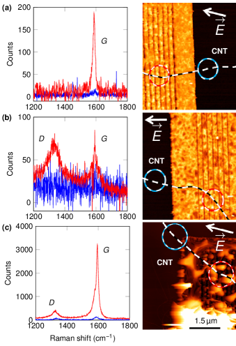
Figure 4 shows the results of Raman measurements performed on three samples. The red curves on the left panels refer to the Raman signal around the and the peak measured on CNT segments located on the antenna strips, while the blue ones correspond to Raman measurements on bare portions. The spectra have been acquired after an integration time of 30 s. The right panels in Fig. 4 show AFM topography scans of the three samples, where the red and light blue circles indicate the laser spot size and location for the bare CNT portion and for the CNT on antennas, respectively. The arrows indicate the incident light polarization for each measurement. The difference between red and blue curves in Fig. 4(a)–(c) clearly shows the dramatic amplification of the Raman signal induced by the optical antennas.
In order to quantify the signal amplification, we define the enhancement factor as the ratio between the Raman peak amplitudes measured with and without antennas. The enhancement factor is difficult to estimate when the signal on the bare portion of the CNT is too weak. The intensity of the Raman signal measured on a bare CNT depends on the difference between the incident (or the scattered ) photon energy and the energy separation between VHSs. The width of such resonance windows is roughly of the order of 200 meV for the mode and around 100 meV for the radial breathing mode (RBM) Maultzsch et al. (2005). If the difference between incident (or scattered) photon and the transition energy is larger than the above values, then the Raman signal is drastically suppressed. This is often the case: for a given laser frequency , only a small fraction of the CNTs shows a significant signal. This is precisely where the advantage of optical antennas becomes obvious, as the signal amplification compensates for the suppression due to the energy mismatch Paradiso et al. (2015). As demonstrated in Fig. 4, also CNTs which are scarcely or not measurable without antennas provide a significant signal. From the spectrum in Fig. 4(a) we deduce an enhancement factor of around 40. While the signal on the bare portion of this CNT is barely discernible, the amplified signal provides useful information: the CNT has a low number of defects, as deduced by the absence of the peak; furthermore the narrow (FWHM: 17 cm-1) peak implies a very weak components, which indicates either an achiral CNT (armchair or zig-zig) or a CNT with very low chiral angle Park et al. (2009).
The graph in Fig. 4(b) refers to a CNT whose Raman spectrum is not measurable on the bare portion even after an integration time of 300 s, i.e. ten times longer than the usual one. This indicates that the CNT has no transitions near 633 nm. However, the signal on the CNT portion suspended on the antennas is clearly detectable, though weak. Since the peak is stronger than the peak, we deduce that this CNT has a relatively high number of defects.
Finally Fig. 4(c) shows the results of Raman measurements on antennas made of Ti/Pt, i.e. without the Re sticking layer. As mentioned above, the absence of the Re sticking layer induce large corrugations in the Pt film when subjected to growth temperatures of the order of 850∘C. We note that despite the surface roughness the enhancement factor remains considerably high, of the order of 60. This particular CNT has a separation between VHSs relatively close to the incident photon energy, thus the Raman signal is large enough to be detected without antennas as well. However, the antenna array allows us to measure also the RBM (not shown). By following the standard assignment procedure we deduce the possible chiral indices for the CNT. We found that the most likely chiral indices are (22,5) or (21,7), two adjacent elements of the CNT family which share very similar properties, as e.g. diameter, chiral angle and energy separation between VHSs [SeetheSupplementalMaterialforfurtherdetails]SMnote1.
III Discussion
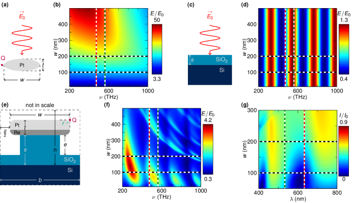
The widths of the plasmonic resonances measured in our reflectance spectroscopy experiments are of the order of nm. As shown below, simple model calculations considering metallic strips alone lead to plasmonic resonance widths much larger than the observed ones. One possibility to explain the observed narrow resonances is to consider in addition the optical interference due to the SiO2/Si interface 470 nm below the sample surface. We will show that the interplay between the optical mode in the SiO2 cavity and the plasmonic mode within the antenna strips gives rise to much sharper eigenmodes. Numerical simulations, discussed at the end of this section, show that such modes have a width comparable to that observed in the experiment.
In our analytical calculation [SeetheSupplementalMaterialforfurtherdetails]SMnote1 we approximate a single strip as an infinitely long cylinder of elliptical cross-section. As sketched in Fig. 5(a) the field is evaluated in the position Q located 5 nm away from the strip edge. The vertical axis measures 25 nm (equal to our antenna thickness) and the horizontal axis is varied. The graph in Fig. 5(b) shows the results of the calculation for the electric field amplitude (normalized to the incident field amplitude) as a function of both and the incident frequency . We notice that, owing to the large imaginary part of the refractive index of Pt Rakić et al. (1998), for all widths the LSPR resonance width is much broader than that observed in our experiment.
In principle, the plasmonic eigenmodes of an array of strips differ from those of a single structure owing to the electrostatic interaction between the strips which leads to mode hybridization. However, such a difference is relevant only if the decay length for the near field amplitude in the vicinity of a strip is comparable to the gap between two adjacent strips. In the visible range such decay length for submicrometric plasmonic structures is of the order of a few nanometers [SeetheSupplementalMaterialforfurtherdetails]SMnote1; Novonty and Hecht (2006), which is much smaller than the gap ( nm). Therefore the interaction between adjacent strips can be neglected in our case.
The sharp minima observed in our reflectance spectroscopy experiment can be explained by considering the effect of the substrate. Indeed, even in a plain SiO2/Si substrate the electric field amplitude at the sample surface strongly depends on the frequency , owing to the optical interference between the two surfaces of the SiO2 film. In Fig. 5(d) we plot the calculated electric field amplitude in a point located on the upper SiO2 surface. For ease of comparison with one of the following figures, the graph is plotted as a function of and as in Fig. 5(b), although in absence of nanoantennas the variable plays no role. The graph shows that the field amplitude at the surface considerably oscillates as a function of the frequency. Clearly, this significantly alters the LSPR profile of optical antennas patterned on top of a SiO2 film.
To quantify the impact of the substrate on the LSPR, we performed a finite-difference frequency-domain (FDFD) numerical simulation on the actual geometry, sketched in Fig. 5(e). In the calculation we model the nanoantennas as periodic arrays of infinitely long strips. By sweeping geometry parameters and laser frequency, we do not only extract field enhancement factors but also identify plasmonic modes and the interplay between the metal structure and the SiO2/Si substrate stack. The strip section is assumed to be rectangular with rounded corners (with radius of curvature nm). The gap nm, the etching depth nm and the SiO2 thickness nm are kept constant. The result of the simulation is plotted in Fig. 5(f). The graph shows the horizontal component of the electric field amplitude calculated in the point Q indicated in the sketch, plotted as a function of width and frequency . A comparison with the graphs in Fig. 5(b) and (d) reveals that the actual eigenmodes are non-trivial combinations of the cavity modes in the SiO2 layer and the plasmonic modes in the metal strip. In fact, the graph in Fig. 5(f) shows a broad feature (on the left and bottom part of the graph) modulated by almost vertical fringes which are clearly related to the SiO2 film interference. As a result, in the visible range the maximum of the near field amplitude for a 200 nm-wide strip occurs at approximately 470 THz, i.e. close to the red laser frequency. We also notice several arc-shaped features on the top-right zone of the graph, which correspond to higher energy-modes. Further details about the calculation and the interpretation of optical modes are given in the Supplemental Material.
The reflection coefficient for a thin film deposited on top of a high refractive index substrate displays a maximum when the electric field at the surface is minimal [SeetheSupplementalMaterialforfurtherdetails]SMnote1. This condition corresponds to a frequency such that the electric field forms a standing wave within the SiO2 layer, with nodes at the two interfaces. Vice versa, when the reflection coefficient is minimal, the electric field at the surface is maximal. On the other hand, when the polarizability of an optical antenna (and thus the near field amplitude) has a maximum as a function of then, due to the imaginary part of the metal refractive index, the reflected far field shows a minimum. From these arguments we expect that the color plot of the reflected far field, shown in Fig. 5(g), will display a reverse contrast when compared to that of the near field shown in Fig. 5(f). In order to compare the simulation results with the white light reflectance spectra, in Fig. 5(g) we plot the intensity as a function of the wavelength and strip width . The line cuts for and 100 nm are shown in Fig. 2(c,d). These latter indicate that the minimum for the reflected signal occurs at nm, the resonance width is approximately 100 nm and that the curve for nm is slightly sharper and slightly blue-shifted compared to the one for nm. These features are in agreement with the experimental data. We notice, however, that the precise shape of the minimum is not suitably captured by the simulation. Note that the exact wavelength for the minimum critically depends on the SiO2 layer thickness. The SiO2 layer thickness is measured with an accuracy of 10 nm, which causes a comparable uncertainty for in the simulation.
A conclusion drawn from the calculations above is that the dependence of the antenna resonance frequency on both antenna width and antenna gap is relatively smooth. Therefore the roughness produced by the CVD process has a negligible effect on both the resonance frequency and the enhancement factor. This can explain the good enhancement factor observed in Fig. 4(c) despite the surface roughness of the metal stripes of that sample.
IV Conclusions
We have demonstrated directional optical antennas for applications that require extremely high process temperatures as, e.g., those required for the CVD growth of CNTs. We have fabricated devices where CNTs are grown on top of antenna arrays and shown that the latter significantly amplify the CNT Raman signal. Numerical simulations show that the relatively sharp antenna resonance is due to the interplay of plasmonic resonance and thin film interference due to the SiO2 cap layer. Possible applications of Pt-Re optical antennas go well beyond SERS of CNTs, since the present fabrication scheme can be in principle applied to any nanostructure for optical spectroscopy whose fabrication requires extreme temperature conditions.
Acknowledgements.
The work was funded by the European Union within the STREP “SE2ND”, and by the Deutsche Forschungsgemeinschaft within Grants No. SFB689 and No. GRK1570.References
- Novonty and Hecht (2006) L. Novonty and B. Hecht, Principles of Nano-Optics (Cambridge University Press, Cambridge, 2006).
- Tame et al. (2013) M. S. Tame, K. R. McEnery, S. K. zdemir, J. Lee, S. A. Maier, and M. S. Kim, Nat. Physics 9, 329 (2013).
- Kneipp et al. (1997) K. Kneipp, Y. Wang, H. Kneipp, L. T. Perelman, I. Itzkan, R. R. Dasari, and M. S. Feld, Phys. Rev. Lett. 78, 1667 (1997).
- Nie (1997) S. Nie, Science 275, 1102 (1997).
- Chikkaraddy et al. (2016) R. Chikkaraddy, B. de Nijs, F. Benz, S. J. Barrow, O. A. Scherman, E. Rosta, A. Demetriadou, P. Fox, O. Hess, and J. J. Baumberg, Nature 535, 127 (2016).
- Moskovits (1985) M. Moskovits, Rev. Mod. Phys. 57, 783 (1985).
- Stosch et al. (2011) R. Stosch, F. Yaghobian, T. Weimann, R. J. C. Brown, M. J. T. Milton, and B. Gttler, Nanotechnology 22, 105303 (2011).
- Kneipp et al. (2004) K. Kneipp, H. Kneipp, M. S. Dresselhaus, and S. Lefrant, Philosophical Transactions of the Royal Society of London A: Mathematical, Physical and Engineering Sciences 362, 2361 (2004).
- Fleischmann et al. (1974) M. Fleischmann, P. J. Hendra, and A. J. McQuillan, Chem. Phys. Lett. 26, 163 (1974).
- Creighton (1982) J. A. Creighton, Surface Enhanced Raman Scattering, (R. K. Chang nad T. E. Furtak editors, Plenum, New York, New York, 1982) p. 315.
- Benner et al. (1983) R. Benner, K. V. Raben, K. Lee, J. Owen, R. Chang, and B. Laude, Chemical Physics Letters 96, 65 (1983).
- Weitz and Oliveria (1984) D. A. Weitz and M. Oliveria, Phys. Rev. Lett. 52, 1433 (1984).
- Sanda et al. (1980) P. N. Sanda, J. M. Warlaumont, J. E. Demuth, J. C. Tsang, K. Christmann, and J. A. Bradley, Phys. Rev. Lett. 45, 1519 (1980).
- Liao et al. (1981) P. Liao, J. Bergman, D. Chemla, A. Wokaun, J. Melngailis, A. Hawryluk, and N. Economou, Chemical Physics Letters 82, 355 (1981).
- (15) .
- Cao et al. (2005) J. Cao, Q. Wang, and H. Dai, Nat. Materials 4, 745 (2005).
- Laird et al. (2015) E. A. Laird, F. Kuemmeth, G. A. Steele, K. Grove-Rasmussen, J. Nygård, K. Flensberg, and L. P. Kouwenhoven, Rev. Mod. Phys. 87, 703 (2015).
- Saito et al. (1998) R. Saito, G. Dresselhaus, and M. S. Dresselhaus, Physical Properties of Carbon Nanotubes (Imperial College Press, London, 1998).
- Kneipp et al. (2000) K. Kneipp, H. Kneipp, P. Corio, S. D. M. Brown, K. Shafer, J. Motz, L. T. Perelman, E. B. Hanlon, A. Marucci, G. Dresselhaus, and M. S. Dresselhaus, Phys. Rev. Lett. 84, 3470 (2000).
- Chu et al. (2009) H. Chu, J. Wang, L. Ding, D. Yuan, Y. Zhang, J. Liu, and Y. Li, Journal of the American Chemical Society 131, 14310 (2009).
- Heeg et al. (2014) S. Heeg, A. Oikonomou, R. Fernandez-Garcia, C. Lehmann, S. A. Maier, A. Vijayaraghavan, and S. Reich, Nano Letters 14, 1762 (2014).
- Paradiso et al. (2015) N. Paradiso, F. Yaghobian, C. Lange, T. Korn, C. Schüller, R. Huber, and C. Strunk, Phys. Rev. B 91, 235449 (2015).
- Cao et al. (2004) J. Cao, Q. Wang, M. Rolandi, and H. Dai, Phys. Rev. Lett. 93, 216803 (2004).
- Dirnaichner et al. (2016) A. Dirnaichner, M. del Valle, K. J. G. Götz, F. J. Schupp, N. Paradiso, M. Grifoni, C. Strunk, and A. K. Hüttel, Phys. Rev. Lett. 117, 166804 (2016).
- Kataura et al. (1999) H. Kataura, Y. Kumazawa, N. Kojima, Y. Y. Maniwa, I. Umezu, S. Masubuchi, S. Kazama, X. Zhao, Y. Ando, Y. Ohtsuka, S. Suzuki, and A. Y., Proceedings of the IWEPNM’99 (American Institute of Physics, Noodbury (NY), 1999).
- Jorio et al. (2001) A. Jorio, R. Saito, J. H. Hafner, C. M. Lieber, M. Hunter, T. McClure, G. Dresselhaus, and M. S. Dresselhaus, Phys. Rev. Lett. 86, 1118 (2001).
- Maultzsch et al. (2005) J. Maultzsch, H. Telg, S. Reich, and C. Thomsen, Phys. Rev. B 72, 205438 (2005).
- Le Thi Ngoc et al. (2013) L. Le Thi Ngoc, M. Jin, J. Wiedemair, A. van den Berg, and E. T. Carlen, ACS Nano 7, 5223 (2013).
- (29) .
- Huang et al. (2003) S. Huang, X. Cai, and J. Liu, Journal of the American Chemical Society 125, 5636 (2003).
- (31) .
- Park et al. (2009) J. S. Park, K. Sasaki, R. Saito, W. Izumida, M. Kalbac, H. Farhat, G. Dresselhaus, and M. S. Dresselhaus, Phys. Rev. B 80, 081402 (2009).
- Rakić et al. (1998) A. D. Rakić, A. B. Djurišić, J. M. Elazar, and M. L. Majewski, Appl. Opt. 37, 5271 (1998).