Quantum Transport in Ambipolar Few-layer Black Phosphorus
Abstract
Few-layer black phosphorus possesses unique electronic properties giving rise to distinct quantum phenomena and thus offers a fertile platform to explore the emergent correlation phenomena in low dimensions. A great progress has been demonstrated in improving the quality of hole-doped few-layer black phosphorus and its quantum transport studies, whereas the same achievements are rather modest for electron-doped few-layer black phosphorus. Here, we report the ambipolar quantum transport in few-layer black phosphorus exhibiting undoubtedly the quantum Hall effect for hole transport and showing clear signatures of the quantum Hall effect for electron transport. By bringing the spin-resolved Landau levels of the electron-doped black phosphorus to the coincidence, we measure the spin susceptibility . This value is larger than for hole-doped black phosphorus and illustrates an energetically equidistant arrangement of spin-resolved Landau levels. Evidently, the n-type black phosphorus offers a unique platform with equidistant sequence of spin-up and spin-down states for exploring the quantum spintronic.
Few-layer black phosphorus, a two-dimensional semiconductor with a tunable direct band gap, is of a growing importance not only for the potential technological applications but also for the fundamental condensed matter studiesXia et al. (2014); Li et al. (2014); Castellanos-Gomez et al. (2014); Qiao et al. (2014); Takao et al. (1981); Ling et al. (2015); Yuan et al. (2015); Buscema et al. (2014a); Wang et al. (2015); Yuan et al. (2016); Rodin et al. (2014); Buscema et al. (2014b); Liu et al. (2015); Low et al. (2014a, b); Churchill and Jarillo-Herrero (2014). A layer-controlled small band gap of few-layer black phosphorus being on the order of a few hundreds of permits tuning the chemical potential between the conduction and valence bands by employing the field effect and thus enables the ambipolar operation of few-layer black phosphorus-based devicesTakao et al. (1981); Akahama et al. (1983); Tran et al. (2014). The development of device fabrication techniques accompanied with the improvement of black phosphorus (BP) crystal quality has experienced a tremendous progressGillgren et al. (2014); Chen et al. (2015); Li et al. (2015); Long et al. (2016a); Tayari et al. (2015). The hole mobility increased from a few hundred to a few thousands Li et al. (2016). A further boost of the hole mobility up to 45,000 has been made when a BP flake is encapsulated between hexagonal boron nitride (h-BN) in vacuumLong et al. (2016b). This high carrier mobility enabled the observation of Shubnikov-de Haas oscillations and the quantum Hall effect in a hole-doped (-type) BP. In spite of these achievements, the performance of electron-doped (-type) BP-based devices remains poor and therefore the electron quantum transport is less explored. According to the theoretical models, the electrons in BP ought to exhibit distinguishable many-body phenomena due to the expected large electron massQiao et al. (2014). Hence, there is a quest to improve the quality of electron-doped black phosphorus crystal and the performance of the devices made thereof, which will eventually lead to the emergence of new quantum phenomena in -type black phosphorus. Here, we take advantage of both encapsulating the BP flakes with h-BN in vacuum conditions and the field effect to control the charge carrier type. The ambipolar device operation demonstrates unambiguously the quantum Hall effect for holes and exhibits clear signatures of quantum Hall effect for electrons.
I Transport characteristics of ambipolar BP devices
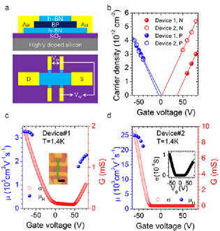
Figure 1a displays the schematic side and top views of the hallbar devices fabricated from h-BN/BP/h-BN heterostructure. The h-BN/BP/h-BN heterostructure is assembled in vacuum to reduce the surface absorption and to minimize the amount of impurities on the BP interfacesLong et al. (2016b). The Ohmic contacts are made of either chromium or titanium because of their work functions being close to conduction and valence band edges of black phosphorus, respectivelyLong et al. (2016a); Perello et al. (2015); Cai et al. (2014). All the conductance channels are along X direction (Supplementary materials). The electrical measurement are performed with standard lock-in technique(Excitation frequency: 4.579Hz). Device1 has Ti as the Ohmic contact metal, whereas device2 has Cr as the Ohmic contact metal (Supplementary materials). The devices show distinct transport characteristics with a controlled charge carrier type, and their high performance are reproducibly demonstrated on several devicesLong et al. (2016a). Figure 1b shows the dependence of the charge carrier density on the gate voltage applied between the conducting substrate acting as a gate electrode and one of the Ohmic contacts. More importantly, it manifests a good tuning capability between the electron and hole charge carrier types. Figure 1c depicts the four-terminal conductance of device1 as a function of the gate voltage at temperature . The conductance increase for positive and negative gate voltages is accompanied with the increasing Hall mobility . Here and are length and width of the device, respectively, and hole (electron) density is estimated from the Hall effect for selected gate voltage values. The Hall mobility for holes and electrons reach 3150 and 2150 at , respectively. Figure 1d summarizes the field effect characteristics of the device2 fabricated with Cr contacts. The transport characteristics measured in a four-terminal configuration shows a typical -type unipolar conductance. The channel conductance increases with the decreasing gate voltage and the Hall mobility reaches 25600 at - comparable with the previous reportLong et al. (2016b). For a positive gate voltage, the measurement of fails likely due to the failure of an Ohmic contact. Note, that the energy difference between the work function of Cr and the Fermi level of black phosphorus is rather large for the -type channel. Nonetheless, the device can be characterized in a two-point measurement, the inset of Figure 1d depicts the two-point conductance. The field effect mobility reaches 850 and 420 for holes and electrons, respectively. These values are obviously underestimated due to the contact resistance. For holes, the Hall mobility obtained in two-point and four-point measurements differs by factor of 50. Thus, assuming the same factor of underestimation for electrons, we can estimate the electron Hall mobility to be on the order 20,000 . A low Hall mobility in device1 is likely caused by the enhanced scattering rate from the impurities and imperfections of the Si substrate. Indeed, the bottom h-BN layer of device1 is only 4.6 and is smaller than 12.3 thick h-BN layer in device2. Thus, the charge carrier transport in device1 is stronger affected by the scattering centers on the Si substrate than device2.
II Ambipolar magnetotransport in BP devices
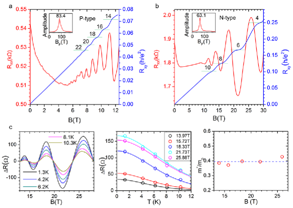
We now turn our attention to demonstrate the ambipolar quantum transport characteristics of both devices in the magnetic field. Figure 2a displays the dependence of and on the magnetic field for hole-type carriers that is obtained upon the application of a backgate voltage on device1. The magnetotransport for electron-type carriers is presented in Figure 2b when a backgate voltage of is applied. The onset of oscillation at for holes and for electrons correspond to a quantum mobility of 2000 and 1000 , respectively. The values approximate the Hall mobility value (Figure 1c) and indicate that the large angle scattering event in this device dominate, likely due to a thin bottom h-BN flakes over the small angle scattering process in this deviceLong et al. (2016b); Coleridge (1991); Piot et al. (2005); Hwang and Sarma (2008); Knap et al. (2004). The insets in Figure 2a and Figure 2b show the fast Fourier transformation (FFT) of as a function of . The peaks of FFT confirms a periodic oscillation of caused by the formation of Landau levels in the high magnetic field. The carrier concentrations extracted from the FFT frequencies agree well with those determined by the Hall resistance manifesting the absence of another parallel conducting channel in both and -type BP. At high magnetic field, exhibits the plateau formations corresponding to the quantum Hall resistance , where is an integer number. These plateaus align well with minimas of . Thus the magnetotransport signals the quantum Hall effect both for -type and -type conductance in BP device. The left panel of Figure 2c shows the temperature dependence of oscillatory component for the -type conduction and reveals the damping of the oscillation amplitude with temperature. This damping behavior follows the Lifshitz-Kosevitch formalism , where is the temperature damping factor, and allows the estimation of the electron effective massShoenberg (2009). The middle panel of Figure 2c shows a fairly good fitting of oscillation amplitude damping using the Lifshitz-Kosevitch formalism. The extracted electron effective mass is and is independent of the magnetic field as shown in Figure 2c right. This value is in consistence with previous reportsLi et al. (2015) and the theoretical predicationsQiao et al. (2014).
The magnetotransport for electron- and hole-type charge carriers shows the conductance quantization at only even filling factors, which suggests that the spin degree of freedom is not resolved even if the magnetic field is high. The discussion of the transport characteristics of device2 presented below may suggest that the high disorder of device1 – reflected in a rather low Hall mobility and a high magnetic field for oscillation onset- can likely account for not observing the lifting of the spin degeneracy. Therefore, this device does not allow to access the spin properties of electrons in black phosphorus.
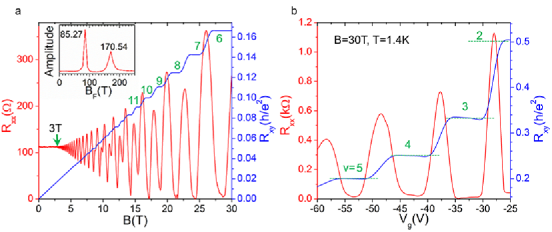
Device2 fabricated with chromium Ohmic contacts has a much higher mobility than observed in device1 suggesting that the level of the disorder is lower and now we turn our attentional to device2. The magnetotransport characteristics for holes in the magnetic field up to are shown in Figure 3a. Here the back gate voltage is and the temperature is . At low magnetic field (), exhibits nearly zero magnetoresistance indicating the bare existence of localizations in the sample and demonstrating the unprecedented quality of the BP device. The onset of oscillation starts at with the sequence of only even Landau level filling factors. This corresponds to a quantum mobility of 3300 which is about 8 times lower than Hall mobility. This suggests that the small angle scattering over remote charge impurities dominates over the large angle scattering due to a thicker h-BN bottom layer in device in device2 than in device1. The splitting of oscillations occurs at and develops rapidly in the magnetic field demonstrating the impact of exchange interactions on the splitting which is associated with lifting the spin degeneracy. The Fourier transformation of periodic oscillations on -axis show two spectra line at and (inset of Figure 3a) and thus confirms the lifting of spin degeneracy. When magnetic field reaches 15T, the zero resistance of as well as the quantized plateaus clearly establish the realization of the quantum Hall effect in -type BP deviceStone (1992). By sweeping the gate voltage at fixed magnetic field one gains an access to lower filling factors. Figure 3b reveals a set of plateaus at values , where assumes an integer number from 2 to 5, accompanied with the zero resistance states. Thus, the Landau level filling factor can be unequivocally assigned to each plateau. The quantum Hall effect observation at both even and odd filling factors confirms the lifting of spin degeneracy at high magnetic field.
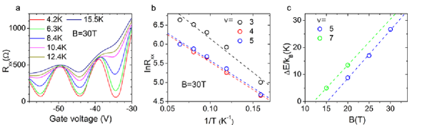
The zero-resistance states demonstrate well-developed quantum Hall states hence enabled the quantitatively study of the thermal activation energy in our BP device. Figure 4a shows the thermal activation of at . Figure 4b displays at three integer Landau level filling factors as a function of . The solid lines represent the fitting results according to the Boltzmann law , where is the activation energy. For black phosphorus the odd filling factors are associated with the Zeeman gap and therefore the activation energy can be expressed as , where is the Landau level broadening. The activation energy at filling factor and depend linearly on the magnetic field . Thus, since both filling factors are associated with the Zeeman gap, the Lande g-factor is estimated to be and for and in hole doped BP, respectively. These values are in good agreement with our previously reported g-factor value obtained through the Landau level coincidence techniqueLong et al. (2016b).
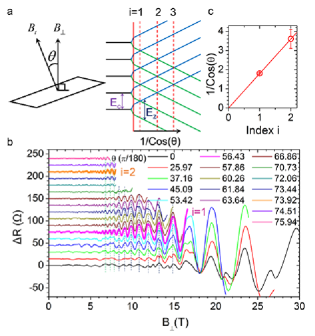
Now we draw our attention to the quantum transport characteristics on the electron side. Although the transport characteristics cannot be obtained in the four-point measurements, the two-point magnetotransport characteristics display the oscillations. The bottom line of figure 5b exemplifies the oscillation component of two-point magnetoresistance with and at zero tilt angle. The charge carrier density is determined from the period of the quantum oscillations. The minima of oscillations correspond to the integer filling factors and the splitting of quantum oscillations starts at . This splitting signals the lifting of spin degeneracy, which hence opens the access to explore the spin properties of electrons in black phosphorus. We now utilize this fact to measure the electron spin susceptibility by bringing the spin-resolved Landau level to the coincidence – so-called coincidence techniqueSchumacher et al. (1998); Kozuka et al. (2012); Maryenko et al. (2014); Tsukazaki et al. (2008); Xu et al. (2017); Long et al. (2016b); Fang and Stiles (1968); Nicholas et al. (1988). This method profits from the fact that the Zeeman energy is given by the total magnetic field , while the cyclotron energy scales with the magnetic field component normal to the the sample plane. Thus and can be controlled individually by tilting the sample in magnetic field. At certain angle , the Zeeman energy is an integer of cyclotron energy, i.e. , the spin resolved Landau levels overlap as shown in Figure 5a. The spin resolved Landau levels cross each other and is the coincidence angle. The spin-susceptibility can be extracted from the coincidence angle condition . Figure 5b displays the evolution of the oscillatory part of the two-point resistance under a constant as and/or tilt angle increases. A coincidence event in the experiment is marked by the vanishing of quantum oscillation components of quantum states at even/odd filling factors i.e. the disappearance of the splitting features. As shown in figure 5b, when the tilt angle approaches even- deeps gradually become weak and finally disappear at . When the tilt angle increases beyond the deep feature reappears. The same evolution takes place at , but with a large uncertainty.The oscillation amplitudes reaches its maxima at both and further confirming the coincidence events at these two anglesKurganova et al. (2011). The coincidence events at and are emphasized by representing with bold lines in figure 5b. Figure 5c plots versus . The linear fit of this dependence yields the spin susceptibility for -type BP . This value of illustrates an energetically equidistant arrangement of spin-resolved Landau levels for high filling factors () at zero tilt angle which makes -type BP an ideal platform to explore spin-related phenomena like quantum-spintronic. Considering the electron effective mass , the Lande g-factor for -type conducting BP is determined to be . The enhanced Lande g-factors have been observed in 2DEGs/2DHGs and can be ascribed to the exchange interactionsNicholas et al. (1988); Kurganova et al. (2011); Shashkin et al. (2001); Zhu et al. (2003); Vakili et al. (2004); Gokmen et al. (2007). This value in -type BP is slightly larger than that in -type conducting BPLong et al. (2016b), which might be ascribed to the enhanced electron-electron interactions due to large effective mass of electronZhou et al. (2017); Girvin (2000); Falson et al. (2015). The interaction strength is gauged by the ratio of the Coulomb energy to the kinetic energy , where n (or p) is carrier density, is the Bohr radius, and is the dielectric constant of surrounding mediumMovva et al. (2017); Maryenko et al. (2015).
In summary, this study demonstrates the quantum Hall effect in the ambipolar operation of the black phosphorus field effect devices. For hole-doped black phosphorus, we demonstrate the unprecedented quality of the device showing no localization effects around zero field. Furthermore, we measured the Lande g-factor by analyzing the excitation gap at odd filling factors. Its value is consistent with the previous report. For black phosphorus with electron-type carriers, The quantum Hall effect is observed and the Landau level crossing has been studied using the standard coincidence technique. The determined electron mass and Lande g-factor illustrate a equidistant sequence of spin-up and spin-down states makes n-type BP an ideal model system for quantum-spintronic applications.
Acknowledgements
We acknowledge the support of the HFML-RU/FOM, member of the European Magnetic Field Laboratory (EMFL).
Financial support from the Research Grants Council of Hong Kong (Project Nos. 16302215, HKU9/CRF/13G, 604112, and N_HKUST613/12), Guangdong-Hong Kong joint innovation project (Grant 2016A050503012) and technical support of the Raith-HKUST Nanotechnology Laboratory for the electron-beam lithography facility at MCPF are hereby acknowledged.
Competing financial interests
The authors declare no competing financial interests.
Author contributions
G. L. and N. W. conceived the project. G. L. fabricated the devices and performed electronic transport measurements with the help of S. P. and U. Z. G. L., D. M., S. p., U. Z., and N. W. analyzed the data and wrote the manuscript. Other authors provided technical assistance in the project.
References
- Xia et al. (2014) F. Xia, H. Wang, and Y. Jia, Nature communications 5, 4458 (2014).
- Li et al. (2014) L. Li, Y. Yu, G. J. Ye, Q. Ge, X. Ou, H. Wu, D. Feng, X. H. Chen, and Y. Zhang, Nature nanotechnology 9, 372 (2014).
- Castellanos-Gomez et al. (2014) A. Castellanos-Gomez, L. Vicarelli, E. Prada, J. O. Island, K. Narasimha-Acharya, S. I. Blanter, D. J. Groenendijk, M. Buscema, G. A. Steele, J. Alvarez, et al., 2D Materials 1, 025001 (2014).
- Qiao et al. (2014) J. Qiao, X. Kong, Z.-X. Hu, F. Yang, and W. Ji, Nature communications 5, 4475 (2014).
- Takao et al. (1981) Y. Takao, H. Asahina, and A. Morita, Journal of the Physical Society of Japan 50, 3362 (1981).
- Ling et al. (2015) X. Ling, H. Wang, S. Huang, F. Xia, and M. S. Dresselhaus, Proceedings of the National Academy of Sciences 112, 4523 (2015).
- Yuan et al. (2015) H. Yuan, X. Liu, F. Afshinmanesh, W. Li, G. Xu, J. Sun, B. Lian, A. G. Curto, G. Ye, Y. Hikita, et al., Nature nanotechnology 10, 707 (2015).
- Buscema et al. (2014a) M. Buscema, D. J. Groenendijk, G. A. Steele, H. S. Van Der Zant, and A. Castellanos-Gomez, Nature Communications 5, 4651 (2014a).
- Wang et al. (2015) X. Wang, A. M. Jones, K. L. Seyler, V. Tran, Y. Jia, H. Zhao, H. Wang, L. Yang, X. Xu, and F. Xia, Nature nanotechnology 10, 517 (2015).
- Yuan et al. (2016) S. Yuan, E. van Veen, M. I. Katsnelson, and R. Roldán, Physical Review B 93, 245433 (2016).
- Rodin et al. (2014) A. Rodin, A. Carvalho, and A. C. Neto, Physical review letters 112, 176801 (2014).
- Buscema et al. (2014b) M. Buscema, D. J. Groenendijk, S. I. Blanter, G. A. Steele, H. S. van der Zant, and A. Castellanos-Gomez, Nano letters 14, 3347 (2014b).
- Liu et al. (2015) H. Liu, Y. Du, Y. Deng, and D. Y. Peide, Chemical Society Reviews 44, 2732 (2015).
- Low et al. (2014a) T. Low, A. Rodin, A. Carvalho, Y. Jiang, H. Wang, F. Xia, and A. C. Neto, Physical Review B 90, 075434 (2014a).
- Low et al. (2014b) T. Low, R. Roldán, H. Wang, F. Xia, P. Avouris, L. M. Moreno, and F. Guinea, Physical review letters 113, 106802 (2014b).
- Churchill and Jarillo-Herrero (2014) H. O. Churchill and P. Jarillo-Herrero, Nature nanotechnology 9, 330 (2014).
- Akahama et al. (1983) Y. Akahama, S. Endo, and S.-i. Narita, Journal of the Physical Society of Japan 52, 2148 (1983).
- Tran et al. (2014) V. Tran, R. Soklaski, Y. Liang, and L. Yang, Physical Review B 89, 235319 (2014).
- Gillgren et al. (2014) N. Gillgren, D. Wickramaratne, Y. Shi, T. Espiritu, J. Yang, J. Hu, J. Wei, X. Liu, Z. Mao, K. Watanabe, et al., 2D Materials 2, 011001 (2014).
- Chen et al. (2015) X. Chen, Y. Wu, Z. Wu, Y. Han, S. Xu, L. Wang, W. Ye, T. Han, Y. He, Y. Cai, et al., Nature communications 6, 7315 (2015).
- Li et al. (2015) L. Li, G. J. Ye, V. Tran, R. Fei, G. Chen, H. Wang, J. Wang, K. Watanabe, T. Taniguchi, L. Yang, et al., Nature nanotechnology 10, 608 (2015).
- Long et al. (2016a) G. Long, S. Xu, J. Shen, J. Hou, Z. Wu, T. Han, J. Lin, W. K. Wong, Y. Cai, R. Lortz, et al., 2D Materials 3, 031001 (2016a).
- Tayari et al. (2015) V. Tayari, N. Hemsworth, I. Fakih, A. Favron, E. Gaufres, G. Gervais, R. Martel, and T. Szkopek, Nature communications 6, 7702 (2015).
- Li et al. (2016) L. Li, F. Yang, G. J. Ye, Z. Zhang, Z. Zhu, W. Lou, X. Zhou, L. Li, K. Watanabe, T. Taniguchi, et al., Nature nanotechnology 11, 593 (2016).
- Long et al. (2016b) G. Long, D. Maryenko, J. Shen, S. Xu, J. Hou, Z. Wu, W. K. Wong, T. Han, J. Lin, Y. Cai, et al., Nano Letters 16 (12), 7768 (2016b).
- Perello et al. (2015) D. J. Perello, S. H. Chae, S. Song, and Y. H. Lee, Nature communications 6, 7809 (2015).
- Cai et al. (2014) Y. Cai, G. Zhang, and Y.-W. Zhang, Scientific Reports 4, 6677 (2014).
- Coleridge (1991) P. Coleridge, Physical Review B 44, 3793 (1991).
- Piot et al. (2005) B. Piot, D. Maude, M. Henini, Z. Wasilewski, K. Friedland, R. Hey, K. Ploog, A. Toropov, R. Airey, and G. Hill, Physical Review B 72, 245325 (2005).
- Hwang and Sarma (2008) E. Hwang and S. D. Sarma, Physical Review B 77, 195412 (2008).
- Knap et al. (2004) W. Knap, V. Fal’ko, E. Frayssinet, P. Lorenzini, N. Grandjean, D. Maude, G. Karczewski, B. Brandt, J. Łusakowski, I. Grzegory, et al., Journal of Physics: Condensed Matter 16, 3421 (2004).
- Shoenberg (2009) D. Shoenberg, Magnetic oscillations in metals (Cambridge University Press, 2009).
- Stone (1992) M. Stone, Quantum Hall Effect (World Scientific, 1992).
- Schumacher et al. (1998) H. Schumacher, A. Nauen, U. Zeitler, R. Haug, P. Weitz, A. Jansen, and F. Schäffler, Physica B: Condensed Matter 256, 260 (1998).
- Kozuka et al. (2012) Y. Kozuka, A. Tsukazaki, D. Maryenko, J. Falson, C. Bell, M. Kim, Y. Hikita, H. Hwang, and M. Kawasaki, Physical Review B 85, 075302 (2012).
- Maryenko et al. (2014) D. Maryenko, J. Falson, Y. Kozuka, A. Tsukazaki, and M. Kawasaki, Physical Review B 90, 245303 (2014).
- Tsukazaki et al. (2008) A. Tsukazaki, A. Ohtomo, M. Kawasaki, S. Akasaka, H. Yuji, K. Tamura, K. Nakahara, T. Tanabe, A. Kamisawa, T. Gokmen, et al., Physical Review B 78, 233308 (2008).
- Xu et al. (2017) S. Xu, J. Shen, G. Long, Z. Wu, Z.-q. Bao, C.-C. Liu, X. Xiao, T. Han, J. Lin, Y. Wu, H. Lu, J. Hou, L. An, Y. Wang, Y. Cai, K. M. Ho, Y. He, R. Lortz, F. Zhang, and N. Wang, Phys. Rev. Lett. 118, 067702 (2017).
- Fang and Stiles (1968) F. F. Fang and P. J. Stiles, Phys. Rev. 174, 823 (1968).
- Nicholas et al. (1988) R. J. Nicholas, R. J. Haug, K. v. Klitzing, and G. Weimann, Phys. Rev. B 37, 1294 (1988).
- Kurganova et al. (2011) E. Kurganova, H. van Elferen, A. McCollam, L. Ponomarenko, K. Novoselov, A. Veligura, B. van Wees, J. Maan, and U. Zeitler, Physical Review B 84, 121407 (2011).
- Shashkin et al. (2001) A. Shashkin, S. Kravchenko, V. Dolgopolov, and T. Klapwijk, Physical review letters 87, 086801 (2001).
- Zhu et al. (2003) J. Zhu, H. Stormer, L. Pfeiffer, K. Baldwin, and K. West, Physical review letters 90, 056805 (2003).
- Vakili et al. (2004) K. Vakili, Y. Shkolnikov, E. Tutuc, E. De Poortere, and M. Shayegan, Physical review letters 92, 226401 (2004).
- Gokmen et al. (2007) T. Gokmen, M. Padmanabhan, E. Tutuc, M. Shayegan, S. De Palo, S. Moroni, and G. Senatore, Physical Review B 76, 233301 (2007).
- Zhou et al. (2017) X. Zhou, W.-K. Lou, D. Zhang, F. Cheng, G. Zhou, and K. Chang, Physical Review B 95, 045408 (2017).
- Girvin (2000) S. M. Girvin, Physics Today 53, 39 (2000).
- Falson et al. (2015) J. Falson, D. Maryenko, B. Friess, D. Zhang, Y. Kozuka, A. Tsukazaki, J. Smet, and M. Kawasaki, Nature Physics 11, 347 (2015).
- Movva et al. (2017) H. C. Movva, B. Fallahazad, K. Kim, S. Larentis, T. Taniguchi, K. Watanabe, S. K. Banerjee, and E. Tutuc, arXiv preprint arXiv:1702.05166 (2017).
- Maryenko et al. (2015) D. Maryenko, J. Falson, M. Bahramy, I. Dmitriev, Y. Kozuka, A. Tsukazaki, and M. Kawasaki, Physical review letters 115, 197601 (2015).