Aggregation of BiTe Monolayer on Bi2Te3(111) Induced by Diffusion of Intercalated Atoms in van der Waals Gap
Abstract
We report a post-growth aging mechanism of Bi2Te3(111) films with scanning tunneling microscopy in combination with density functional theory calculation. It is found that a monolayered structure with a squared lattice symmetry gradually aggregates from surface steps. Theoretical calculations indicate that the van der Waals (vdW) gap not only acts as a natural reservoir for self-intercalated Bi and Te atoms, but also provides them easy diffusion pathways. Once hopping out of the gap, these defective atoms prefer to develop into a two dimensional BiTe superstructure on the Bi2Te3(111) surface driven by positive energy gain. Considering the common nature of weakly bonding between vdW layers, we expect such unusual diffusion and aggregation of the intercalated atoms may be of general importance for most kinds of vdW layered materials.
Studies on bismuth chalcogenide (Bi2X3) have long been focused regarding the potential in thermoelectricity Wright (1958), and also been revived recently by the discovery of topological insulators (TIs) Moore (2010); Qi and Zhang (2011); Hasan and Kane (2010); Zhang et al. (2009a); Hsieh et al. (2009a); Chen et al. (2009); Hsieh et al. (2009b); Wang et al. (2011); Kim et al. (2016). It has been confirmed that most Bi2X3 compounds, such as Bi2Te3, Bi2Se3 and Sb2Se3, are prototypical 3D TIs Zhang et al. (2009a); Chen et al. (2009); Hsieh et al. (2009a, b). Hosting the topological surface states and gapped bulk band structure, Bi2X3 becomes promising in the future applications such as quantum computation and spintronic etc Moore (2010); Qi and Zhang (2011); Hasan and Kane (2010).
In spite of the robustness of the topological surface states against time-reversal invariant perturbation, temporal stability of the surface or interface still greatly affects the Bi2X3’s performance and application. Intensive studies have been conducted regarding the surface atomistic and band structure evolution upon exposing to various gases including air Benia et al. (2011); Chen et al. (2012a); Koleini et al. (2013); Edmonds et al. (2014); Zhang et al. (2016); Atuchin et al. (2011, 2016), however it still remains elusive whether and how the Bi2X3 intrinsically evolves in ultrahigh vacuum (UHV). ARPES studies indicated that a long stay in UHV induces an energy band splitting Benia et al. (2011). A low-energy ion scattering (LEIS) study confirmed a way of surface degradation of Bi2Se3, i.e., the cleaved surface in UHV undergoes a fast Se evaporation and is thus terminated by Bi bilayer He et al. (2013). It was also observed that annealing induces the surface segregation of Bi bilayer Coelho et al. (2013). Therefore, a direct characterization of surface evolution upon long term exposure in UHV is important, which, however, hasn’t been reported yet.
In this Letter, we demonstrate a post-growth aggregation on Bi2Te3(111) surface induced by the self-intercalation and diffusion of Bi and Te atoms in the van der Waals (vdW) gap with scanning tunneling microscopy (STM) in combination with density functional theory (DFT) calculation. We observe that upon long term aging, a monolayered Mosaic pattern, presumably composed of Bi and Te, is gradually formed starting at the step edges of Bi2Te3(111) surface. DFT calculations confirm that Bi atoms prefer to be intercalated in the vdW gap between quintuple layers (QLs) than being adsorbed on the surface, and the difference between the formation energy of Bi and Te intercalated atoms in the gap is smaller than that on the surface. The diffusion barriers of the intercalated atoms in the vdW gap are also comparable to those on the surface. We therefore suggest that the vdW gap acts as a reservoir for the bulk defect Bi and Te atoms with thermally activated diffusion pathways. The lateral segregation of the intercalated atoms from the steps leads to a BiTe monolayered structure on Bi2Te3 (111) surface. Furthermore, elastic relaxation due to the stress mismatch between BiTe monolayer and Bi2Te3 surface forms a Mosaic pattern in the BiTe monolayer. In contrast to the previous studies about the surface stability, which are mainly surface decomposition or reaction He et al. (2013); Coelho et al. (2013), this work presents a long term effect induced by the bulk intercalated atoms. Since intercalation of atoms commonly exist in vdW gaps Eknapakul et al. (2014); Moutaabbid et al. (2016), it is expected that such a novel mechanism may exist in other layered materials as well, considering the intrinsic nature of vdW interactions.
Thin Bi2Te3 films were grown by molecular beam epitaxy (MBE) in UHV with a Unisoku LT-STM-MBE joint system. The base pressure is mbar. Bi2Te3(111) films were grown on the Si(111)- substrate at 260∘C, and 2 monolayers (MLs) of Te buffer layer was deposited prior to the Bi2Te3(111) film growth. The as-grown Bi2Te3 film was kept in UHV without any further processing prior to STM scan. STM measurements were performed at 80 K. Constant current mode was adopted, and a mechanically polished PtIr tip was applied.
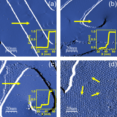
Figure 1 shows the temporal evolution of the surface morphology of Bi2Te3 films upon aging in UHV. The as-grown Bi2Te3 film, as shown in Fig. 1(a), is terminated by the spiral steps and atomically flat surface terraces. The step height of Bi2Te3 is 1 nm, consistent with Bi2Te3 crystal structure and previous report Zhang et al. (2009b). Upon long term exposure in UHV, a superstructure starts to develop. Figures 1(b) to (d) show the surface morphology after aging in UHV for four days, six days and thirteen days, respectively. The newly formed structure prefers to nucleate adjacent to the Bi2Te3 steps and grows laterally in the lower terrace. The coverage of superstructure increases with the aging time. The thickness of the superstructure is kept at 0.2 nm, as measured in the insets of Fig. 1(b) and (c), implying that the superstructure is a monolayered structure. Moreover, as marked by the yellow arrows in Fig. 1(d), there exists three equivalent domains in the superstructure, oriented 120∘ with each other.
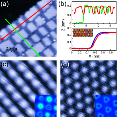
Zoom-in images indicate that the superstructure features the ribbon-like structure. The width of the ribbons is distributed uniformly at 2.5 nm, as illustrated by the green line in Fig. 2(a) and the scan profile in Fig. 2(b). There also exists depressions along the ribbons, with a corrugation of 0.1 nm. The lateral interspace distribution of these depressions varies from 1.5 nm to 5.0 nm, as illustrated by the red line in Fig. 2(a) and blue scan profile in Fig. 2(b). Atomically resolved STM image of the superstructure, Fig. 2(c), shows a nearly squared periodicity, different from the hexagonal symmetry in the Bi2Te3(111) surface, Fig. 2(d).
It is well known that Bi forms bilayer islands on top of Bi2Te3 surface, with a thickness of 0.4 nm Chen et al. (2012b); Coelho et al. (2013), much larger than the superstructure’s thickness of 0.2 nm. Pure Te on Bi2Te3 surface forms islands or clusters near the surface steps Hoefer et al. (2015), in contrast to the observed monolayered superstructure as well. In addition, the symmetry of Bi and Te adlayer structures are both hexagonal Chen et al. (2012b); Coelho et al. (2013); Hoefer et al. (2015), not in the squared periodicity as observed in Fig. 2(c). Therefore, we rule out the possibility that the superstructure is composed of either pure Bi or pure Te. According to the alloy phase diagram of BimTen Baker (1992), the plausible candidate with a squared lattice symmetry should be the (001) termination of metastable BiTe phase, which takes a rock-salt structure in a space group Baker (1992). Therefore, we propose that the superstructure is composed of both Bi and Te atoms in the BiTe phase.
Since the superstructure forms in the post-growth aging process, it is reasonable to assume that both the required Te and Bi atoms originate within the intercalated atoms from the as-grown Bi2Te3 layers. To verify such a mechanism, we need to check the following questions: (1) How can the atoms be stored as defects in a bulk? (2) How can the atoms migrate freely to the surface in aging? To address these issues, we conduct first-principles DFT calculations to compare the formation and diffusion process of Bi and Te atoms in the bulk and on the surface, respectively.
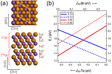
The DFT calculations Payne et al. (1992) were performed with the Vienna Ab Initial Simulation Package (VASP) using the projector augmented wave method Kresse and Furthmüller (1996); Kresse and Joubert (1999). The Perdew-Burke-Ernzerhoff exchange-correlation functional with the semiempirical vdW correction based on Grimmes scheme (PBE-D2) Grimme (2006); Barone et al. (2009); Grimme et al. (2010); Luo et al. (2012) was employed, with an energy cutoff of 300 eV and no spin-orbit coupling effect included Luo et al. (2012). With these settings, the lattice parameters of bulk Bi2Te3 is a = 4.34 and c = 31.71 , which agrees well with the experimental values Nakajima (1963). The Bi2Te3(111) surface was modeled by using a supercell Hashibon and Elsässer (2011); Zhang et al. (2013) consisting of a three-QL slab and a vacuum with thickness of 12 , as shown in Fig. 3(a). The surface brillouin zone was sampled with a -centered mesh, which has been tested to be well converged. The positions of atoms in the bottom QL were fixed to mimic the bulk, and the other atoms were relaxed until the forces were converged to 0.01 eV/. A larger supercell with a k-mesh sampling is used to check the size convergence. The difference is 60 meV at maximum in formation energies of Bi atoms at high-symmetrical sites of the surface and within the vdW gap. STM images were simulated using the Tersoff and Hamann approximation Tersoff and Hamann (1985).
As the inter-QL interaction is vdW type, much weaker than the expected covalent bonding within the QLs, it is intuitive to consider the vdW gap as a possible reservoir to adopt the Te and Bi defect atoms. We thus compare the formation energy of intercalated Te and Bi atoms in the vdW gap and that of adatoms on the surface. The formation energy of a defect complex containing Bi and Te atoms depends on the chemical potential of Bi and Te components. Assuming the approximate equilibrium of the chemical potential of Bi2Te3 and those of Bi and Te, we obtain the following,
| (1) |
where , with and the total energy of the Bi2Te3 host system with and without the defect atoms, respectively. are the free energy per atom in the bulk Bi (Te) metal. is the formation energy of bulk Bi2Te3 in reference to the bulk metals. The upper and lower bounds of , the chemical potential of Te in reference to the bulk Te metal, are determined by the formation of Te metal and Bi metal, respectively. According to our calculation, .
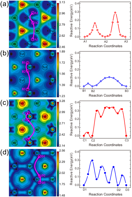
The potential energy surface (PES) of Bi and Te adatom on the surface in Te-rich limit are plotted in Fig. 4(a) and (b) respectively, , . Similar PES of Bi and Te in the vdW gap are plotted in Fig. 4(c) and (d). Obviously, the formation of Bi adatom is less favorable than that of Te adatom by 1.23 eV. The formation of intercalated Bi in the vdW gap is also less favorable than that of Te, but only by 0.65 eV. Note that the minimum sites both on the surface and in the gap deviate evidently from the sites of high symmetry.
It is interesting to note that in Te-rich condition, the formation of Bi defect atom is much easier in the vdW gap than on the surface, by 0.32 eV. In comparison, formation of Te defect atom is less favorable in the gap than on the surface by 0.26 eV. Therefore the difference between the probability of forming Bi and Te defect atoms in the gap is quite smaller than on the surface. This difference decreases with decreasing , as shown in Fig. 3(b). The intercalation of Bi and Te atoms becomes equally favorable in the vdW gap at of eV. It means that the number ratio of Bi and Te intercalated in the gap approaches to 1:1 when the number of Bi adatoms is still much smaller than that of Te adatoms on the surface.
In addition to the formation energy, the diffusion barriers of the defect atoms are also important because they determine the dynamics during the aging process. The nudged elastic band (NEB) method Mills et al. (1995) is used to obtain the accurate diffusion barrier for the diffusion pathways based on the PES, as illustrated by the red curves in Fig. 4. The limiting barriers for the diffusion of Bi and Te atom on the surface are obtained to be 0.28 eV (A2-A3) and 0.11 eV (B2-B3), respectively. Comparatively, the diffusion barriers of Bi and Te atom in the gap are 0.34 eV (C2-C3) and 0.30 eV (D1-D2), respectively. It is obvious that the diffusion barriers of both Bi and Te atoms in the vdW gap are still small enough for thermal activation during the aging process.
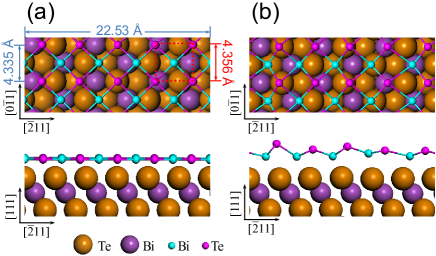
Combining the DFT results and experiments, it follows that a monolayered BimTen with :2:3 can be formed as a result of the lateral segregation of intercalated Bi and Te atoms from the vdW gap. The aforementioned BiTe satisfies the condition. The lattice parameters of an free-standing BiTe monolayer is 4.356 according to our calculation. In comparison, the lattice constant of the Bi2Te3(111) surface is 4.335 and 3.755 along and , respectively. Obviously it is well commensurate along the direction of Bi2Te3 with the BiTe monolayer. We thus construct the BiTe/Bi2Te3(111) interface using a slab with a supercell of Bi2Te3(111) surface which accommodates atop BiTe supercell, as shown in Fig. 5.
The BiTe monolayer after relaxation becomes slightly undulated, with the average distance of 3.71 and 2.79 away from the surface for Te and Bi atoms, respectively. However, it is worthy to note that the monolayer still keeps the original squared periodicity, consistent with the experimental observation. The formation energy of a BiTe monolayer on the Bi2Te3(111) surface is calculated to be 0.44 eV per atom under the Te-rich condition, which is quite smaller than that of an isolated Bi or Te defect atom either on the surface or in the gap. It follows that once the diffusion of the defects is thermally activated, Bi and Te defect atoms tend to aggregate and form a BiTe monolayer. Note that the BiTe supercell may have three equivalent orientation 120∘ with each other due to the hexagonal symmetry of the substrate, which is consistent with the experimental observations. We also construct a slab with a BiTe supercell on the supercell of Bi2Te3(111) surface to model the step height of the BiTe monolayer. As shown in Fig. 2(b), the obtained 2.3 is well consistent with the experimental result.
It is well-known that a monolayer is unstable against the formation of domains via elastic relaxation if there is a mismatch between the surface stress of the monolayer and that of the substrateShchukin and Bimberg (1999). The instability wavelength in a specific direction can be roughly estimated as follows Srolovitz (1989); Alerhand et al. (1988),
| (2) |
For present system, is the lattice constant of the BiTe monolayer, the edge energy, the Young modulus, and is the stress tensor difference between the Bi2Te3(111) surface with and without the BiTe monolayer. We can assume , where and are the surface energy of Bi2Te3(111) surface and the thickness of the BiTe monolayer, respectively. According to our calculation, eV/, GPa and GPa along the and directions, respectively. Thus, we obtain the instability wavelength as 18 and 32 in and directions, respectively, which are consistent with the typical length scale of the Mosaic pattern observed experimentally.
In summary, we demonstrate for the first time a post-growth aging effect on Bi2Te3 (111) surface in UHV, i.e. the aggregation of BiTe monolayer on Bi2Te3 (111) surface, which is facilitated by the low formation energy and the thermally activated diffusion of intercalated Bi and Te atoms in the vdW gap. In contrast to the previous studies which can be well explained by surface decomposition or reaction, this study uncovers an intrinsic process originated from a novel diffusion process of the defects within the vdW gaps. Considering the common nature of weakly bonding between vdW layers, we expect such unusual formation, diffusion and aggregation of defects may be of general importance for the stability and performance of devices based on most kinds of vdW layered materials.
This work was supported by the Ministry of Science and Technology of China (Grants No.2014CB921103 and No. 2013CB922103),the National Natural Science Foundation of China (Grants No. 11374140, No. 11174123,No. 11474157, No. 11674155 and No. 11634005), the Basic Research Project of Jiangsu Province(Grant No. BK20161390) and the Open Research Fund Program of the State Key Laboratory of Low-Dimensional Quantum Physics. The numerical calculations were carried out at the National Supercomputing Center in Tianjin.
Z.-W. W. and W.-K. H. contributed equally to this work.
References
- Wright (1958) D. A. Wright, Nature (London) 181, 834 (1958).
- Moore (2010) J. E. Moore, Nature (London) 464, 194 (2010).
- Qi and Zhang (2011) X. L. Qi and S. C. Zhang, Rev. Mod. Phys. 83, 1057 (2011).
- Hasan and Kane (2010) M. Z. Hasan and C. L. Kane, Rev. Mod. Phys. 82, 3045 (2010).
- Zhang et al. (2009a) H. Zhang, C. X. Liu, X. L. Qi, X. Dai, Z. Fang, and S. C. Zhang, Nat. Phys. 5, 438 (2009a).
- Hsieh et al. (2009a) D. Hsieh, Y. Xia, D. Qian, L. Wray, J. H. Dil, F. Meier, J. Osterwalder, L. Patthey, J. G. Checkelsky, N. P. Ong, et al., Nature (London) 460, 1101 (2009a).
- Chen et al. (2009) Y. L. Chen, J. G. Analytis, J. H. Chu, Z. K. Liu, S. K. Mo, X. L. Qi, H. J. Zhang, D. H. Lu, X. Dai, Z. Fang, et al., Science 325, 178 (2009).
- Hsieh et al. (2009b) D. Hsieh, Y. Xia, D. Qian, L. Wray, F. Meier, J. H. Dil, J. Osterwalder, L. Patthey, A. V. Fedorov, H. Lin, et al., Phys. Rev. Lett. 103, 146401 (2009b).
- Wang et al. (2011) G. Wang, X. G. Zhu, Y. Y. Sun, Y. Y. Li, T. Zhang, J. Wen, X. Chen, K. He, L. L. Wang, X. C. Ma, et al., Adv. Mater. 23, 2929 (2011).
- Kim et al. (2016) K. C. Kim, J. Lee, B. K. Kim, W. Y. Choi, H. J. Chang, S. O. Won, B. Kwon, S. K. Kim, D. B. Hyun, H. J. Kim, et al., Nat. Commun. 7, 12449 (2016).
- Benia et al. (2011) H. M. Benia, C. Lin, K. Kern, and C. R. Ast, Phys. Rev. Lett. 107, 177602 (2011).
- Chen et al. (2012a) C. Chen, S. He, H. Weng, W. Zhang, L. Zhao, H. Liu, X. Jia, D. Mou, S. Liu, J. He, et al., Proc. Natl. Acad. Sci. U.S.A. 109, 3694 (2012a).
- Koleini et al. (2013) M. Koleini, T. Frauenheim, and B. Yan, Phys. Rev. Lett. 110, 016403 (2013).
- Edmonds et al. (2014) M. T. Edmonds, J. T. Hellerstedt, A. Tadich, A. Schenk, K. M. O’Donnell, J. Tosado, N. P. Butch, P. Syers, J. Paglione, and M. S. Fuhrer, J. Phys. Chem. C 118, 20413 (2014).
- Zhang et al. (2016) K. W. Zhang, D. Ding, C. L. Yang, Y. Gan, S. Li, W. K. Huang, Y. H. Song, Z. Y. Jia, X. B. Li, Z. Zhu, et al., Phys. Rev. B 93, 235445 (2016).
- Atuchin et al. (2011) V. V. Atuchin, V. A. Golyashov, K. A. Kokh, I. V. Korolkov, A. S. Kozhukhov, V. N. Kruchinin, S. V. Makarenko, L. D. Pokrovsky, I. P. Prosvirin, K. N. Romanyuk, et al., Cryst. Growth Des. 11, 5507 (2011).
- Atuchin et al. (2016) V. V. Atuchin, V. A. Golyashov, K. A. Kokh, I. V. Korolkov, A. S. Kozhukhov, V. N. Kruchinin, I. D. Loshkarev, L. D. Pokrovsky, I. P. Prosvirin, K. N. Romanyuk, et al., J. Solid State Chem. 236, 203 (2016).
- He et al. (2013) X. He, W. Zhou, Z. Y. Wang, Y. N. Zhang, J. Shi, R. Q. Wu, and J. A. Yarmoff, Phys. Rev. Lett. 110, 156101 (2013).
- Coelho et al. (2013) P. M. Coelho, G. A. S. Ribeiro, A. Malachias, V. L. Pimentel, W. S. Silva, D. D. Reis, M. S. C. Mazzoni, and R. Magalh ̵̡ es-Paniago, Nano Lett. 13, 4517 (2013).
- Eknapakul et al. (2014) T. Eknapakul, P. D. King, M. Asakawa, P. Buaphet, R. H. He, S. K. Mo, H. Takagi, K. M. Shen, F. Baumberger, T. Sasagawa, et al., Nano Lett. 14, 1312 (2014).
- Moutaabbid et al. (2016) H. Moutaabbid, Y. Le Godec, D. Taverna, B. Baptiste, Y. Klein, G. Loupias, and A. Gauzzi, Inorg. Chem. 55, 6481 (2016).
- Zhang et al. (2009b) T. Zhang, P. Cheng, X. Chen, J. F. Jia, X. Ma, K. He, L. Wang, H. Zhang, X. Dai, Z. Fang, et al., Phys. Rev. Lett. 103, 266803 (2009b).
- Chen et al. (2012b) M. Chen, J. P. Peng, H. M. Zhang, L. L. Wang, K. He, X. C. Ma, and Q. K. Xue, Appl. Phys. Lett. 101, 081603 (2012b).
- Hoefer et al. (2015) K. Hoefer, C. Becker, S. Wirth, and L. H. Tjeng, AIP Adv. 5, 097139 (2015).
- Baker (1992) H. Baker, ed., ASM Handbook: Vol. 3 Alloy Phase Diagrams (ASM International, Ohio, 1992).
- Payne et al. (1992) M. C. Payne, M. P. Teter, D. C. Allan, T. A. Arias, and J. D. Joannopoulos, Rev. Mod. Phys. 64, 1045 (1992).
- Kresse and Furthmüller (1996) G. Kresse and J. Furthmüller, Phys. Rev. B 54, 11169 (1996).
- Kresse and Joubert (1999) G. Kresse and D. Joubert, Phys. Rev. B 59, 1758 (1999).
- Grimme (2006) S. Grimme, J. Comput. Chem. 27, 1787 (2006).
- Barone et al. (2009) V. Barone, M. Casarin, D. Forrer, M. Pavone, M. Sambi, and A. Vittadini, J. Comput. Chem. 30, 934 (2009).
- Grimme et al. (2010) S. Grimme, J. Antony, S. Ehrlich, and H. Krieg, J. Chem. Phys. 132, 154104 (2010).
- Luo et al. (2012) X. Luo, M. B. Sullivan, and S. Y. Quek, Phys. Rev. B 86, 184111 (2012).
- Nakajima (1963) S. Nakajima, J. Phys. Chem. Solids 24, 479 (1963).
- Hashibon and Elsässer (2011) A. Hashibon and C. Elsässer, Phys. Rev. B 84, 144117 (2011).
- Zhang et al. (2013) J. M. Zhang, W. Ming, Z. Huang, G. B. Liu, X. Kou, Y. Fan, K. L. Wang, and Y. Yao, Phys. Rev. B 88, 235131 (2013).
- Tersoff and Hamann (1985) J. Tersoff and D. R. Hamann, Phys. Rev. B 31, 805 (1985).
- Mills et al. (1995) G. Mills, H. Jónsson, and G. K. Schenter, Surf. Sci. 324, 305 (1995).
- Shchukin and Bimberg (1999) V. A. Shchukin and D. Bimberg, Rev. Mod. Phys. 71, 1125 (1999).
- Srolovitz (1989) D. Srolovitz, Acta Metall. 37, 621 (1989).
- Alerhand et al. (1988) O. L. Alerhand, D. Vanderbilt, R. D. Meade, and J. D. Joannopoulos, Phys. Rev. Lett. 61, 1973 (1988).