Two-dimensional superconductivity at the \hkl(111)\ceLaAlO3/\ceSrTiO3interface
Abstract
We report on the discovery and transport study of the superconducting ground state present at the \hkl(111)\ceLaAlO3/\ceSrTiO3 interface. The superconducting transition is consistent with a Berezinskii-Kosterlitz-Thouless transition and its 2D nature is further corroborated by the anisotropy of the critical magnetic field, as calculated by Tinkham. The estimated superconducting layer thickness and coherence length are and , respectively. The results of this work provide new insight to clarify the microscopic details of superconductivity in LAO/STO interfaces, in particular in what concerns the link with orbital symmetry.
Transition metal oxide interfaces host a rich spectrum of functional properties which are not present in their parent bulk constituents Hwang et al. (2012). Following the groundbreaking discovery of a high-mobility two-dimensional electron system (2DES) at the interface between the two wide band-gap insulators \ceLaAlO3 (LAO) and \ceSrTiO3 (STO) Ohtomo and Hwang (2004), a growing body of research efforts have brought to light many of its interesting properties. The system features a gate tunable metal-to-insulator transitionThiel et al. (2006); Cen et al. (2008), strong Rashba spin-orbit coupling Caviglia et al. (2010) and superconductivityReyren et al. (2007), possibly in coexistence with magnetismBert et al. (2011); Li et al. (2011). To date, the vast majority of research efforts has been directed towards the investigation of the \hkl(001)-oriented LAO/STO interface. However, it is well recognized that the direction of confinement plays a pivotal role in determining hierarchy of orbital symmetries and, consequently, in properties such as the spatial extension of the 2DES and the Rashba spin-orbit fields Herranz et al. (2015). Recent work suggests that \hkl(111)-oriented \ceABO3 perovskites are potentially suitable for the realization of topologically non-trivial phases Xiao et al. (2011), since along this direction a bilayer of \ceB-site ions forms a honeycomb lattice. The 2DES at the \hkl(111)LAO/STO interface Herranz et al. (2012) is an interesting subject of investigation, combining a polar discontinuity at the interface with such a hexagonal lattice. Signatures of the 6-fold symmetry related to the \hkl(111)STO orientation have recently been observed by angle-resolved photoemission spectroscopy Rödel et al. (2014); Walker et al. (2014) (ARPES) and magnetoresistanceMiao et al. (2016); Rout et al. (2017) measurements, making the system potentially suitable for exotic time-reversal symmetry breaking superconductivityScheurer, Agterberg, and Schmalian (2017). Moreover, ARPES measurements at the surface of \hkl(111)STO have confirmed a distinct orbital ordering of the manifoldRödel et al. (2014), where all the bands are degenerate at the -point. This implies the absence of a Lifshitz point, considered to be at the origin of many physical properties at the \hkl(001)-oriented interface. In particular, the ‘optimal doping’ for superconductivity was found to occur concomitantly with the Lifshitz transition Joshua et al. (2012). Therefore, within this view, it is timely to investigate whether a 2D superconducting ground state arises at the \hkl(111) orientation.

The \hkl(111)LAO/STO interface under investigation was prepared by pulsed laser deposition. An LAO film with a thickness of 9 unit cells (u.c.) was epitaxially grown on a commercially available \hkl(111)STO substrate with Ti-rich surface. The film was deposited at in an oxygen pressure of . The laser pulses were supplied by a KrF excimer source with an energy density of and a frequency of . The growth process was followed by an annealing step in order to refill oxygen vacancies. The chamber was filled with of oxygen and the sample temperature was kept at for 1 hour. The sample was then cooled down to room temperature at a rate of in the same oxygen atmosphere. The growth process was monitored in-situ using reflection high-energy electron diffraction (RHEED), which indicates a layer-by-layer growth mode, as shown in Figure 1a. An atomic force microscope (AFM) topographic image of the surface after growth is shown in Figure 1b, where an atomically flat surface with step-and-terrace structure can be observed. The step height corresponds to the \hkl(111)STO interplanar distance (). Transport measurements were carried out in a Hall bar geometry, as shown in Figure 1c. The fabrication process relied on argon dry etching in order to define the channel and e-beam evaporation of metal contacts (for a detailed description, see Supporting Information). Hall bars were patterned along different in-plane orientations (, , , and ) in order to investigate possible anisotropies in the transport properties.

The temperature dependence of the sheet resistance () is shown in Figure 2a, evidencing a clear metallic behavior and absence of carrier localisation down to . At this temperature the back gate voltage is swept to the maximum applied voltage () and back to . At variance with previous reports, we observed no hysteretic or anisotropic transport behavior attributed to the presence of oxygen vacancies Davis et al. (2016). All further measurements presented in this work are shown for one Hall bar recorded at a fixed back gate voltage of . The detailed investigation of the evolution of the transport properties with electrostatic doping shall be discussed elsewhere.
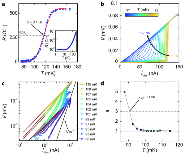
In the milliKelvin regime, a superconducting transition with a critical temperature is observed (Figure 2a). The value of was defined as the temperature at which the resistance is 50% of its normal state value (, measured at ). The width of the transition, defined between 20% and 80% of , is .
For a 2D system, it is well established that superconductivity should exhibit a Berezinskii-Kosterlitz-Thouless (BKT) transition, at a characteristic temperature . Below this temperature, vortex-antivortex pairs are formed. As the temperature increases and approaches , a thermodynamic instability occurs and the vortex-antivortex pairs spontaneously unbind into free vortices. The resulting proliferation of free vortices destroys superconductivity, yielding a finite-resistance state. According to the BKT scenario, a strong non-Ohmic behavior in the characteristics emerges near , following a power law behavior with at .
In order to investigate the 2D character of superconductivity in the system, we measured the characteristics of a 9 u.c. \hkl(111)LAO/STO interface as a function of temperature. The characteristics were recorded from , where the samples are completely superconducting, up to the temperature at which the sample fully recovers to the normal state. As shown in Figure 2b, there is a clear superconducting current plateau for the curve at . As the temperature is increased, the supercurrent plateau becomes progressively shorter, until it vanishes at approximately . At this temperature, the curve becomes completely linear. Concomitantly with the disappearance of the superconducting plateau, power-law type curves emerge, indicating a BKT transition. In order to confirm this scenario, we plot the characteristics on a logarithmic scale, as shown in Figure 2c. At sufficiently low current, the characteristics display Ohmic behaviour in the entire temperature range due to well-known finite size effects Kosterlitz and Thouless (1972, 1973). At higher current values, the curves show a clear power-law dependence, as indicated by the red lines. The black line corresponds to . The exponents are obtained by fitting all the characteristics and are plotted as a function of temperature in Figure 2d, revealing that . At , at low currents, transitioning to a strongly non-linear behaviour at higher currents and showing the characteristic rounding. In contrast, at the power-law behaviour terminates abruptly with a voltage jump at a well defined current. It should be noted that the evolution of does not display the characteristic discontinuous jump from to , but rather transitions smoothly from 1 to 3 over a range of several milliKelvin. This behaviour, also observed in \hkl(001)- and \hkl(110)-oriented interfaces Reyren et al. (2007); Han et al. (2014), stems from inhomogeneties in the local superconducting properties of the system (such as inhomogeneous superfluid density Bert et al. (2012) or structural twin domains of the STO substrate Noad et al. (2016)) which smear the universal jump Baity et al. (2016).

For a quantitative estimation of both the superconducting coherence length () and the layer thickness , we carried out an analysis based on the Landau-Ginzburg formalism. To this purpose, a quantitative criterion was chosen in order to determine the out-of-plane () and in-plane () critical magnetic fields. At each temperature, characteristics are recorded for increasing values of applied magnetic field. As shown in the Supporting Information, for small applied magnetic fields, the values of are zero at low currents, corresponding to the superconducting state. As the current rises, increases until a saturating value, , which corresponds to the normal state resistance. For larger applied magnetic fields, is non-zero, and its value increases with the magnitude of the applied magnetic field.
We define the critical magnetic field as the value at which reaches of the normal state resistance, i.e., .
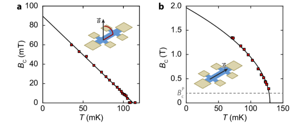
We track the temperature evolution of the critical magnetic field for the out-of-plane and in-plane orientations, which are shown in Figure 3a and b, respectively. The black lines represent a fit to the expected dependence for a 2D superconductor, i.e.,
| (1) |
and
| (2) |
From the extrapolation of the critical magnetic fields at , we extracted the in-plane coherence length and the thickness of the superconducting layer . The fact that the superconducting coherence length is larger than the estimated thickness is consistent with the 2D character of superconductivity.
In fact, can seemingly go far beyond the Pauli paramagnetic limit, which gives a higher bound for the upper critical magnetic field resulting from field-induced pair-breaking Chandrasekhar (1962); Clogston (1962). For weak coupling Bardeen-Cooper-Schrieffer (BCS) superconductors, this value is given by
| (3) |
where is the Boltzmann’s constant and is the Bohr magneton.
Violation of the paramagnetic limit has been observed in \hkl(001)- and \hkl(110)-oriented LAO/STO interfacesHan et al. (2014); Reyren et al. (2009); Shalom et al. (2010), as well as in other STO-based superconductors Kim et al. (2012). In these systems, the paramagnetic limit is exceeded by a factor of approximately -. In our case, we find , which results in a violation of the Pauli paramagnetic limit by a factor of 10, since . As a matter of fact, the violation is already present at temperatures very close to , as shown by the dashed line in Figure 3b. The enhancement of well beyond the BCS prediction has been reported in superconductors which display strong spin-orbit effects Lu et al. (2013); Khim et al. (2011); Gardner et al. (2011). These are expected to cause randomization of electron spins, and thus result in suppression of the effect of spin paramagnetism Maki (1966). Indeed, we have confirmed the presence of strong spin-orbit fluctuations in the system by magnetotransport measurements (see Supporting Information), suggesting that spin-orbit coupling plays an important role in the violation of the Pauli paramagnetic limit.

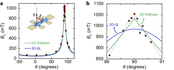
To further investigate the dimensionality of the superconducting layer, we have studied the angular dependence of the critical magnetic field at . Figure 4a shows the critical magnetic field as a function of the angle , defined between the magnetic field vector and the normal to the surface. The data was fitted with the 2D Tinkham formula (green curve) and the 3D anisotropic Ginzburg-Landau model (blue curve), given by
| (4) |
and
| (5) |
respectively.
For the overall range, the data seems to be well described by both models. However, a closer look at the region around in Figure 4b reveals a clear difference between the two models: the 3D model yields a rounded maximum when the magnetic field vector is completely in plane, while the observed cusp-shaped peak can only be well captured by the 2D model.
In summary, by means of systematic (magneto)transport measurements we have demonstrated that the electrons hosted at the \hkl(111)LAO/STO interface condense into a superconducting ground state with . The estimated thickness of the 2D superconducting layer is approximatelly , very similar to the one usually reported for \hkl(001)-oriented interfaces. The characteristics are consistent with a BKT transition, and the two-dimensional character of the superconducting layer was further corroborated by the angular dependence of the critical magnetic field. The Pauli paramagnetic limit is exceeded by a factor of 10, indicating strong spin-orbit coupling in the system. In view of the differences between the symmetries, electronic structure, and orbital ordering of the confined states at the \hkl(001)- and \hkl(111)-oriented LAO/STO interfaces, further investigation of the latter can extend the current understanding of the link between orbital symmetry and superconductivity at LAO/STO interfaces.
Acknowledgements.
We thank T. Baturina for fruitful discussions on the BKT analysis and T. Kool for technical support. This work was supported by The Netherlands Organisation for Scientific Research (NWO/OCW) as part of the Frontiers of Nanoscience program (NanoFront), by the Dutch Foundation for Fundamental Research on Matter (FOM). The research leading to these results has received funding from the European Research Council under the European Union’s H2020 programme/ ERC GrantAgreement n. [677458].References
- Hwang et al. (2012) H. Hwang, Y. Iwasa, M. Kawasaki, B. Keimer, N. Nagaosa, and Y. Tokura, Nature Materials 11, 103 (2012).
- Ohtomo and Hwang (2004) A. Ohtomo and H. Hwang, Nature 427, 423 (2004).
- Thiel et al. (2006) S. Thiel, G. Hammerl, A. Schmehl, C. Schneider, and J. Mannhart, Science 313, 1942 (2006).
- Cen et al. (2008) C. Cen, S. Thiel, G. Hammerl, C. Schneider, K. Andersen, C. Hellberg, J. Mannhart, and J. Levy, Nature Materials 7, 298 (2008).
- Caviglia et al. (2010) A. Caviglia, M. Gabay, S. Gariglio, N. Reyren, C. Cancellieri, and J.-M. Triscone, Physical Review Letters 104, 126803 (2010).
- Reyren et al. (2007) N. Reyren, S. Thiel, A. Caviglia, L. F. Kourkoutis, G. Hammerl, C. Richter, C. Schneider, T. Kopp, A.-S. Rüetschi, D. Jaccard, m. Gabay, D. Muller, J.-M. Triscone, and J. Mannhart, Science 317, 1196 (2007).
- Bert et al. (2011) J. Bert, B. Kalisky, C. Bell, M. Kim, Y. Hikita, H. Hwang, and K. Moler, Nature Physics 7, 767 (2011).
- Li et al. (2011) L. Li, C. Richter, J. Mannhart, and R. Ashoori, Nature Physics 7, 762 (2011).
- Herranz et al. (2015) G. Herranz, G. Singh, N. Bergeal, A. Jouan, J. Lesueur, J. Gázquez, M. Varela, M. Scigaj, N. Dix, F. Sánchez, and J. Fontcuberta, Nature Communications 6, 6028 (2015).
- Xiao et al. (2011) D. Xiao, W. Zhu, Y. Ran, N. Nagaosa, and S. Okamoto, Nature Communications 2, 596 (2011).
- Herranz et al. (2012) G. Herranz, F. Sánchez, N. Dix, M. Scigaj, and J. Fontcuberta, Scientific Reports 2, 758 (2012).
- Rödel et al. (2014) T. Rödel, C. Bareille, F. Fortuna, C. Baumier, F. Bertran, P. Le Fèvre, M. Gabay, O. H. Cubelos, M. Rozenberg, T. Maroutian, P. Lecoeur, and A. Santander-Syro, Physical Review Applied 1, 051002 (2014).
- Walker et al. (2014) S. Walker, A. De La Torre, F. Bruno, A. Tamai, T. Kim, M. Hoesch, M. Shi, M. Bahramy, P. King, and F. Baumberger, Physical Review Letters 113, 177601 (2014).
- Miao et al. (2016) L. Miao, R. Du, Y. Yin, and Q. Li, Applied Physics Letters 109, 261604 (2016).
- Rout et al. (2017) P. Rout, I. Agireen, E. Maniv, M. Goldstein, and Y. Dagan, arXiv:1701.02153 (2017).
- Scheurer, Agterberg, and Schmalian (2017) M. S. Scheurer, D. F. Agterberg, and J. Schmalian, npj Quantum Materials 9, 2 (2017).
- Joshua et al. (2012) A. Joshua, S. Pecker, J. Ruhman, E. Altman, and S. Ilani, Nature Communications 3, 1129 (2012).
- Davis et al. (2016) S. Davis, Z. Huang, K. Han, T. Venkatesan, and V. Chandrasekhar, Advanced Materials Interfaces (2016).
- Kosterlitz and Thouless (1972) J. Kosterlitz and D. Thouless, Journal of Physics C: Solid State Physics 5, L124 (1972).
- Kosterlitz and Thouless (1973) J. M. Kosterlitz and D. J. Thouless, Journal of Physics C: Solid State Physics 6, 1181 (1973).
- Han et al. (2014) Y.-L. Han, S.-C. Shen, J. You, H.-O. Li, Z.-Z. Luo, G.-L. Li, C.-J.and Qu, C.-M. Xiong, R.-F. Dou, L. He, D. Naugle., G.-P. Guo, and J. Nie, Applied Physics Letters 105, 192603 (2014).
- Bert et al. (2012) J. A. Bert, K. C. Nowack, B. Kalisky, H. Noad, J. R. Kirtley, C. Bell, H. K. Sato, M. Hosoda, Y. Hikita, H. Y. Hwang, and K. A. Moler, Phys. Rev. B 86, 060503 (2012).
- Noad et al. (2016) H. Noad, E. M. Spanton, K. C. Nowack, H. Inoue, M. Kim, T. A. Merz, C. Bell, Y. Hikita, R. Xu, W. Liu, et al., Phys. Rev. B 94, 174516 (2016).
- Baity et al. (2016) P. G. Baity, X. Shi, Z. Shi, L. Benfatto, and D. Popović, Phys. Rev. B 93, 024519 (2016).
- Chandrasekhar (1962) B. Chandrasekhar, Applied Physics Letters 1, 7 (1962).
- Clogston (1962) A. Clogston, Physical Review Letters 9, 266 (1962).
- Reyren et al. (2009) N. Reyren, S. Gariglio, A. Caviglia, D. Jaccard, T. Schneider, and J.-M. Triscone, Applied Physics Letters 94, 112506 (2009).
- Shalom et al. (2010) M. Shalom, M. Sachs, D. Rakhmilevitch, A. Palevski, and Y. Dagan, Physical Review Letters 104, 126802 (2010).
- Kim et al. (2012) M. Kim, Y. Kozuka, C. Bell, Y. Hikita, and H. Hwang, Physical Review B 86, 085121 (2012).
- Lu et al. (2013) Y. Lu, T. Takayama, A. F. Bangura, Y. Katsura, D. Hashizume, and H. Takagi, Journal of the Physical Society of Japan 83, 023702 (2013).
- Khim et al. (2011) S. Khim, B. Lee, J. W. Kim, E. S. Choi, G. R. Stewart, and K. H. Kim, Phys. Rev. B 84, 104502 (2011).
- Gardner et al. (2011) H. J. Gardner, A. Kumar, L. Yu, P. Xiong, M. P. Warusawithana, L. Wang, O. Vafek, and D. G. Schlom, Nature Physics 7, 895 (2011).
- Maki (1966) K. Maki, Physical Review 148, 362 (1966).