Thermotronics: toward nanocircuits to manage radiative heat flux
Abstract
The control of electric currents in solids is at the origin of the modern electronics revolution which has driven our daily life since the second half of 20th century. Surprisingly, to date, there is no thermal analog for a control of heat flux. Here, we summarize the very last developments carried out in this direction to control heat exchanges by radiation both in near and far-field in complex architecture networks.
I Introduction
The control of electric currents in solids is at the origin of modern electronics which has revolutionized our daily life. The diode and the transistor introduced by Braun Braun and Bardeen Bardeen are undoubtedly the corner stones of modern information technologies. Such devices allow for rectifying, switching, modulating and even amplifying the electric current. Beside these developements, in the mid 1890s, Tesla’s work Tesla on its remotely-controlled device also called "telautomaton" conceived electronically tunable components with respect to the value of external excitations (electromotrice forces) giving rise to the very first logic gates.
Astonishingly, similar devices which would make possible the control of heat flow do not exist in our current life. An important step forward in this direction has been carried out in 2006 by Baowen Li and co-workers et al. Casati1 by introducing phononic counterpart of a field-effect transistor. In their device, composed as its electronic analog, of three interconnected solid elements, the temperature bias plays the role of the voltage bias and the heat currents carried by phonons play the role of the electric currents. Later, several prototypes of phononic thermal logic gates BaowenLi2 as well as thermal memories BaowenLi3 ; BaowenLiEtAl2012 have been developed in order to process information by phononic heat currents rather than by electric currents. Beside these results, different phononic thermal rectifiers have been proposed BaowenLi2004 ; Chang to introduce an asymmetry in the heat transport with respect to the sign of the temperature gradient Starr1936 ; RobertsWalker2011 opening so the way to the development of thermal diodes.
However, this transport of heat with phonons in solid networks suffers from some weaknesses of fundamental nature which intrinsically limit its performances. One of these limitations is linked to the speed of acoustic phonons itself which is limited by the speed of sound in solids. Another intrinsic limitation of phononic devices is the presence of local Kapitza resistances which come from the mismatch of vibrational modes supported by the different solid elements in the network. This resistance can drastically reduce the heat flux transported across the system.
In this paper we discuss a photonic alternative to the phononic technology by making a review of the latest developments in this direction showing the possibility to realize thermal analogs of electronic fundamental building blocks such as thermal transistor, thermal memory and thermal logic gates for controlling the flow of heat by radiation, storing thermal energy and even making logical operations using thermal photons instead of electrons. Finally, we suggest new research directions for advanced thermal management by tuning radiative heat exchanges in many-body systems using magnetic fields.
II Thermal transistor
As outlined in the introduction, a purely photonic technology has been proposed as an alternative to the phononic one. An important step forward in this direction has been carried out by Fan et al. OteyEtAl2010 by introducing the first radiative thermal rectifier by exploiting the thermal dependence of optical properties of materials in interaction. During the next five years the rectification performances have been improved BasuFrancoeur2011 ; NefzaouiEtAl2013 ; Zhang2 ; Huang ; Dames ; Zhu2 until the development of a phase-change radiative thermal diode able to rectify 66% of heat flux in far-field PBA_APL ; Ito and even more than 99% in the near-field regime van Zwol1 , respectively. Contrary to the relatively weak dependence with respect to the temperature of optical properties of materials used in the thermal rectifier developed so far, the phase-change thermal diode exploites a sudden change of these properties around a critical temperature, the transition temperature.
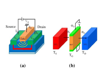
Following this idea, a general concept of radiative transistor has been introduced in 2014 PBA_PRL2014 and applied in 2015 JoulainAPL2015 in the particular situation where only propagating photons participate to the transfer. Before introducing it, let us briefly describe the classical electronic transistor. This last is sketched in Fig. 1(a). It is composed by three solid elements, the drain, the source, and the gate. It is basically used to control the flux of electrons exchanged in the channel between the drain and the source by changing the voltage bias applied on the gate. While, the physical diameter of this channel is fixed its effective electrical diameter can be tuned by application of a voltage on the gate. A tiny change in this voltage can cause a large variation in the current from the source to the drain.
.
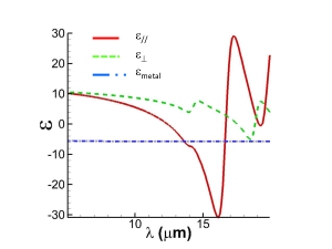
The radiative analog of an electronic transistor PBA_PRL2014 is depicted in Fig. 1(b). It basically consists in a source and a drain, labeled by the indices S and D, which are maintained at temperatures and (which play an analog role as the voltage) using thermostats where so that a net heat flux is transferred from the source towards the drain. A thin layer of a metal-isulator transition material (MIT) labeled by G of width is placed between the source and the drain at a distance from both media and operates as a gate. This configuration coincides with two heat-radiation diodes PBA_APL which are connected in series, so that the heat radiation transistor corresponds to a bipolar transistor. In a MIT material a small change in the temperature around its critical temperature causes a sudden qualitative and quantitative change in its optical properties. Vanadium dioxide (VO2) is one of such materials (see Fig. 2) which undergoes a first-order transition (Mott transition Mott ) from a high-temperature metallic phase to a low-temperature insulating phase Baker close to room-temperature (). Different works have shown van Zwol1 ; van Zwol2 ; vanZwol3 that the heat-flux exchanged at close separation distances (i.e. in the near-field regime) between an MIT material and another medium, can be modulated by several orders of magnitude across the phase transition of MIT materials.
.
Without external excitation, the system will reach its steady state for which the net flux received by the intermediate medium, the gate, is zero by heating or cooling the gate until it reaches its steady state or equilibrium temperature . In this case the gate temperature is set by the temperature of the surrounding media, i.e. the drain and the source. When a certain amount of heat is added to or removed from the gate for example by applying a voltage difference through a couple of electrodes as illustrated in Fig. 1(b) or by extracting heat using Peltier elements, its temperature can be either increased or reduced around its equilibrium temperature . This external action on the gate allows to tailor the heat flux between the source and the gate and the heat flux between the gate and the drain.
To show that this system operates as a transistor let us examinate how the radiative heat flux evolves in this system with respect to the gate temperature. In a three-body system the radiative flux received by the drain takes the form Messina ; Messina2
| (1) |
where the spectral heat flux is given by
| (2) |
Here, and denote the transmission coefficients of each mode between the source and the gate and between the gate and the drain for both polarization states . In the above relation denotes the difference of functions and , being the mean energy of a Planck oscillator at temperature . According to the N-body near-field heat transfer theory Messina ; Messina2 , the transmission coefficients and of the energy carried by each mode written in terms of optical reflection coefficients () and transmission coefficients of each basic element of the system and in terms of reflection coefficients ( and ) of couples of elementary elements is given by ()
| (3) |
introducing the imaginary part of the wavevector normal to the surfaces in the multilayer structure . Similarly the heat flux from the source towards the gate reads
| (4) |
where the transmission coefficients are analog to those defined in Eq. (3) and can be obtained making the substitution . Note that here we have neglected the contribution of the propagating waves which is vanishingly small compared to the contribution of the evanescent waves for distances much smaller than the thermal wavelength. At steady state, the net heat flux received/emitted by the gate which is just given by the heat flux from the source to the gate minus the heat flux from the gate to the drain vanishes so that
| (5) |
This relation allows us to identify the gate equilibrium temperature (which is not necessarily unique because of the presence of bistability mechanisms PBA_PRL2014 ) for given temperatures and . Note that out of steady state, the heat flux received/emitted by the gate is . If () an external flux is added to (removed from) the gate by heating (cooling).
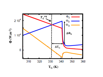
The different operating modes of the transistor can be analyzed from the evolution of flux curves with respect to the gate temperature. These curves are plotted in Fig. 3 in the case of a silica source and a silica drain with a VO2 gate in between. We set and and choose a separation distance between the source and the gate and between the gate and the drain to . The thickness of the gate layer is set to .
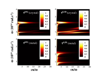
The equilibrium temperature of the gate, obtained by solving the transcendental equation (5) is for this configuration uniquely given by which is close to the critical temperature of VO2. Hence,in the steady-state situation, the gate is in its insulating phase. In this situation it supports surface phonon-polaritons van Zwol1 ; PBA_PRL2014 in the mid-infrared range as well as the source and the drain so that these surface waves can couple together making the heat transfer very efficient between the source and the drain which can be seen by inspection of the transmission coefficients in Fig.4. On the contrary, when the temperature of the gate is increased by external heating to values larger than then VO2 undergoes a phase transition towards its metallic phase. In this case, the gate does not support surface wave resonances anymore so that the surface mode coupling between each solid element is suppressed (see Fig.4) and the heat transfer drastically drops (Fig. 3). This drastic change in the transfer of energy can be used to modulate the heat flux received by the drain by changing the gate temperature around its critical value. The thermal inertia of the gate as well as its phase transition delay defines the timescale at which the switch can operate. Usually the thermal inertia limits the speed to some microseconds Tschikin ; Dyakov2 or even less OrdonezEtAl2016 .
.
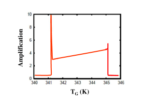
But more interesting is the possibility offered by this system to amplify the heat flux received by the drain. This effect is the thermal analog of the classical transitor effect. To highlight this effect, let us focus our attention on the operating mode in the region of phase transition around . As we see in Fig. 3 a small increase of leads to a drastic reduction of flux received by the drain. As described by Kats et al. in Ref. Kats this behavior can be associated in far-field to a reduction of the thermal emission. This anomalous behavior corresponds to the so called negative differential thermal conductance as described in Fan . The presence of a negative differential thermal conductance is a necessairy condition (but not sufficient) for observing a transistor effect. Indeed, the amplification coefficient of a transistor is defined as (see for example Ref. Casati1 )
| (6) |
where
| (7) |
By introducing the thermal resistances
| (8) |
and
| (9) |
associated to the drain and to the source this coefficient can be recasted under the form
| (10) |
It immediately follows from this expression that when both resistances are positive, then . This, precisely happens outside the phase transition region (see Fig. 3) where so that (Fig. 5). On the contrary, in the region where the phase transition occurs this situation changes. A direct inspection of flux in this region (Fig. 3) clearly shows that and have the same (negative) sign so that and . It turns out that (Fig. 5).
III Radiative memory
In 1946 Williams and Kilburn developed a memory to store data electronically using a cathode ray tube. The basic idea of their invention is summarized in Fig. 6(a). A small electrostatic charge appears on the surface of a screen lighted up by an electron beam and this charge remains for a short period of time before leaking away. This invention constitutes the first volatile memory. Information is stored as long as the charge is not dissipated. In this section, we describe the possibility to store information or energy for arbitrary long time using thermal photons Slava . The concept of thermal memory is closely related to the thermal bistability of a system, i.e. the presence of at least two equilibrium temperatures BaowenLi3 .
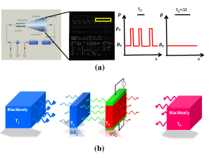
To illustrate this, let us consider the system as depicted in Fig. 6(b) composed by two parallel homogeneous membranes made of VO2 and SiO2. These slabs have finite thicknesses and and are separated by a vacuum gap of distance . The left (right) membrane is illuminated by the field radiated by a blackbody of temperature (), where . The membranes themselves interact on the one hand through the intracavity fields and on the other with the field radiated by the two black bodies.
The heat flux across any plane parallel to the interacting surfaces can be evaluated using Rytov’s fluctuational electrodynamics Rytov ; Polder . Here, we consider the situation where the separation distance is large enough compared to the thermal wavelengths [i.e. , ] so that near-field heat exchanges can be neglected (for a thermal memory working in near-field regime see Ref. DyakovMemory ). In this case we obtain
| (11) |
where the field correlators
| (12) |
of local field amplitudes in polarization can be expressed Slava in terms of reflection and transmission operators and of the layer toward the right () and the left (), as
| (13) |
with
| (14) |
Here denotes the normal component of wave vector in the medium of consideration. Using expression (11) we can calculate the net flux [ ] received by the first (second) membrane.
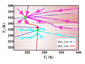
The phase portrait of two membranes plotted in Fig. 7 shows all the time evolution of SiO2 and VO2 membranes for all initial conditions. In this figure, the dashed blue (solid red) line represents the local equilibrium temperatures for the first (second) membrane that is the set of temperatures couples () which satisfy the condition []. The intersection of these two lines define the global steady-state temperatures of the system. It clearly appears that the system possesses three equilibrium temperatures. However, as shown in Slava with the help of a stability study of the system, only two of three equilibrium points that appear in Fig. 7 are stable.
The two stable thermal states can naturally be identified to the "0" and "1" of one bit of information. As long as the temperatures of the two reservoirs are held constant, the system remains in the same stable thermal state. By perturbating the system (for instance by adding or extracting a certain power to one membrane) it is possible to switch from one thermal state to the other state as shown in Fig. 8. The temporal dynamics of temperatures and of the two membranes are solution of the energy balance equation
| (15) |
where we have introduced the vectors , , and . In this nonlinear system of coupled differential equations () is the power per unit volume which can be added to or extracted from both membranes by applying a voltage difference through a couple of electrodes as illustrated in Fig. 6 or by using Peltier elements. In the vector, the terms (i=1,2) represent the thermal inertia of both membranes where and denote the heat capacity and the mass density of each material [see Suppl. Mat. of Ref. Slava for more details].
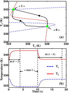
The resolution of this system from the two different initial conditions corresponding to the equilibrium states allows us to describe the dynamics of the switching process between one state and the other one. Here below we briefly describe this writing-reading procedureSlava . To this end, we consider the SiO2-VO2 system made with membranes of equal thicknesses which are coupled to two reservoirs of temperatures and . Let us define "0" as the thermal state at the temperature . To make the transition towards the thermal state "1" the VO2 membrane must be heated.
Step 1 (transition from the state "0" to the state "1"): A volumic power is added to this membrane during a time interval to reach a region in the plane () [see Fig. 8(a)] where all trajectories converge naturally (i.e. for ) after some time toward the state "1", the overall transition time is [see Fig. 8(b)].
Step 2 (maintaining the stored thermal information): Since the state "1" is a fixed point, the thermal data can be maintained for arbitrary long time provided that the thermal reservoirs are switched on.
Step 3 (transition from the state "1" to the state "0"): Finally, a volumic power is extracted from the VO2 membrane during a time interval to reach a region [below in Fig. 8(a)] of natural convergence to the state "0" . In this case the transition time becomes . Compared with its heating, the cooling of VO2 does not follow the same trajectory [see Fig. 8(a)] outlining the hysteresis of the system which accompanies its bistable behavior. To read out the thermal state of the system a classical electronic thermometer based on the thermal dependence of the electric resistivity of membranes can be used.
These results show that many-body radiative systems could be used as volatile thermal memory. The radiative bistability which exists in some of these media can be exploited for energy storage both at macroscale (far-field regime) and subwavelength scale (near-field regime). This thermal energy could in principle release heat upon request in its environment making these systems active building blocks for a smart management of heat exchanges between different objects without any contact.
IV Logic gates with thermal photons
The next-generation of internet of things infrastructures has the potential to change the way people and systems live in a world of massive and disparate data sources, and to provide opportunities for connectivity at different scales. Instead of using electrical signals, purely thermal signals could be used. However the development of such a technology requires the existence of thermal logic gates being able to perform a boolean information treatment as their electronic counterpart do. In this section we demonstrate that NOT, OR and AND gates can be realized exploiting the radiative heat exchanges in N-body systems with phase-change materials PBA_PRL_logic . To start, let us consider the simplest logic gate, the NOT gate which implements a logical negation. This operation can be performed by using the simple termal transistor discussed before [see Fig. 1(b)]. In order to operate as a NOT gate the temperature of the source is maintained at a fixed temperature .
Then, as shown in Fig. 9, the temperature of the intermediate layer plays the same role as an input while the drain temperature acts as an output and defining the thermal state with as the ’0’ state and the termal state with as the ’1’ state, then the system works as a NOT gate. The input state can be controlled from outside by adding or removing heat from the intermediate gate layer.
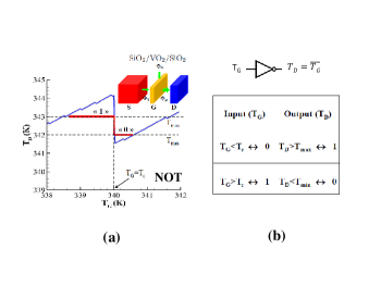
The dynamics of a NOT gate for passing from one state to another (given two different values for corresponding to ’0’ and ’1’) can be evaluated by solving the nonlinear dynamical equation
| (16) |
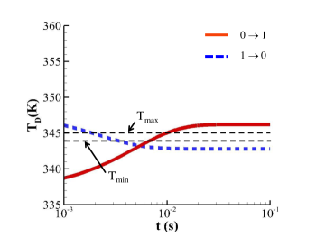
where is the flux received by the drain while , and denote the mass density, the heat capacity and the thickness of the drain, respectively. In Fig. 10 we show the transition dynamics from the state ’0’ to the state ’1’ (from the state ’1’ to the state ’0’) with an initial temperature ( ) and a gate at fixed temperature (). The overall time the NOT gate takes to switch from state ’0’ to state ’1’ (state ’1’ to state ’0’) is on the order of a few ms. Note that compared with the operating speed of electric logic gates this time is large because of the thermal inertia. Nevertheless to activate thermal sensors this delay is largely sufficient.
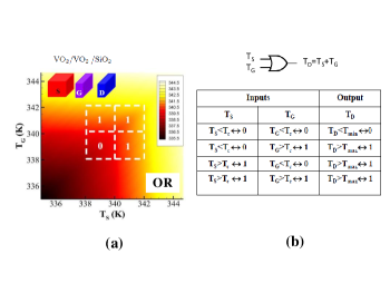
Now let us show that a many-body system can also operate as an OR gate. Note that we consider here, contrary to the NOT gate, a transistor with a phase-change material for both the source and the gate layer while silica is used for the drain layer. The temperatures of the source and the gate are used as inputs while the drain temperature sets the output of the logic gate. The temperature evolution of the drain with respect to the temperatures of the source and the gate is plotted in Fig. 11. We see that around the point with where the phase change occurs both in the source and the gate, the temperature of the drain undergoes a significant variation. If and are both smaller than the critical temperature of VO2 then these two elementary blocks behave like a dielectric so that the temperature of the drain is small. On the contrary, if either the source or the gate undergo a phase change, then the temperature of the drain increases abruptly. Hence, by conveniently intoducing two suitable threshold temperatures and it is clear that we can associate to the drain two different thermal states with respect to the temperatures and around the region . Therefore, this transistor behaves like an OR gate with the truth table given in Fig. 11(b). Note also that by reversing the definition of thermal states in the drain, this system mimicks a NOR gate.
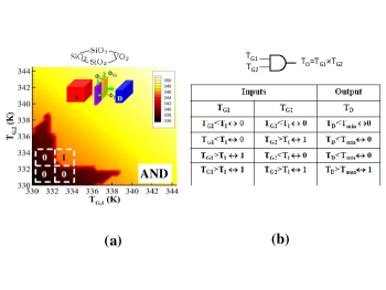
Finally, we sketch the realization of an AND gate. This double input device is shown in Fig. 12(a). It is a double gate thermal transistor made with two silica gates and a silica source. Contrary to the NOT gate it is the drain which is made of a phase-change material. The temperatures of both gates set the two inputs of the logic gate. We assume that the temperatures of the two gates can now be controlled independently making the assumption, for convenience, that they are thermally insulated one from the other so that we can express the heat flux received by the drain just as the mean value of two NOT gates, i.e. we have
| (17) |
Here the transmission coefficients are given by the same expressions as in (3) for a single gate transistor. In Fig. 12(a) we show the equilibrium temperature of the drain with respect to the gate temperatures. In the central region around with we see that can undergo a sudden variation after a short change in the gate temperatures. By introducing two critical temperatures and we can associate to the drain two thermal states ’0’ or ’1’ with respect to the relative value of the drain temperature to these thresholds. As it clearly appears in Fig 12(a). this double gate system behaves as a digital AND gate with the truth table given in Fig. 12(b). Note that by reversing the definition of thermal states ’0’ and ’1’ the AND gate works as a NAND gate. To go beyond this elementary logical operation a combination of various logical gates will now be necessary. However, in near-field regime this combination cannot be sequential, because of many-body effects which make the heat transport throughout the structure non additive.This demands for the development of a general many-body theory.
V magnetic control of heat flux
In this last section we discuss the last developments on the tunability of radiative heat transfer in N-body systems. Although the radiative heat transport along nanoparticle systems have been intensively studied Brongersma ; PBAAPL2006 ; PBAPRB2008 ; Ordonnez2016 since two decades, the external control of radiative heat transfers in complex networks remains largely an open problem. Here below we discuss the possibility, recently demonstrated PBAHall , of a strong tunability of heat transfers in magneto-optical networks with an external magnetic field. This magnetic control of heat flux is associated to the presence of a photon thermal Hall effect in these systems.
The classical Hall effect Hall discovered by Edwin Hall at the end of the 19th century results in the appearance of a transverse electric current inside a conductor under the action of an external magnetic field applied in the direction orthogonal to the primary voltage gradient. This effect comes from the Lorentz force which acts transversally on the electric charges in motion through the magnetic field curving so their trajectories. Very shortly after this discovery, a thermal analog of this effect has been observed by Righi and Leduc Leduc when a temperature gradient is applied throughout an electric conductor. As for the classical Hall effect, this effect is intrinsically related to the presence of free electric charges. So, one can not expect a thermal Hall effect with neutral particles. Nevertheless, during the last decade researchers have highlighted such an effect in non-conducting materials due to phonons Strohm ; Jin or magnons (spin waves) Hirschberger ; Fujimoto ; Katsura ; Onose .
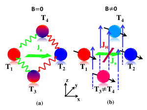
Here below we investigate the near-field heat exchanges in a four-terminal system (see Fig. 13) which is composed of magneto-optical particles under the action of a constant magnetic field applied perpendicularly to the system. Those particles can exchange electromagnetic energy between them. By connecting the two particles along the -axis to two heat baths at two different temperatures, a heat flux flows through the system between these two particles. Without external magnetic field (Fig. 13(a)) all particles are isotropic, so that the two others unthermostated particles have, for symmetry reasons, the same equilibrium temperatures and therefore they do not exchange heat flux through the network. On the contrary, when a magnetic field is applied orthogonally to the particle network (Fig. 13(b)), the particles become anisotropic so that the symmetry of the system is broken (Fig. 1). As we will see hereafter, when the steady-state regime is reached, the two unthermostated particles display two different temperatures. Therefore a heat flux propagates transversally to the primary applied temperature gradient.
Using the Landauer formalism for N-body systems PBAEtAl2011 ; Riccardo ; PRL_superdiff ; Nikbakht ; Incardone the heat flux exchanged between the and the particle in the network reads
| (18) |
where denotes the transmission coefficient, at the frequency , between the two particles. When the particles are small enough compared with their thermal wavelength ( is the vacuum light velocity, is Planck’s constant, and is Boltzmann’s constant) they can be modeled by simple radiating electrical dipoles. In this case the transmission coefficient is defined as Nikbakht
| (19) |
where , and are the susceptibility tensor plus two matrices which read Nikbakht in terms of free space Green tensor (, is the vector linking the center of dipoles i and j, while and stands for the unit dyadic tensor) and of polarizabilities matrix ( being the polarizability tensorAlbaladejo associated to the object)
| (20) |
| (21) |
with and
| (22) |
In Fig. 14 we show the relative Hall temperature difference
| (23) |
in a InSb-particle system Palik with respect to the magnitude of magnetic field for a separation distance (i.e. near-field regime) when the particles of radius are surrounded by vacuum. When the magnetic field is zero, all particles are isotropic so that the system is symmetric and, as expected, . On the contrary, for non-zero magnetic field the symmetry of system is broken and a Hall flux appears (Fig. 13).
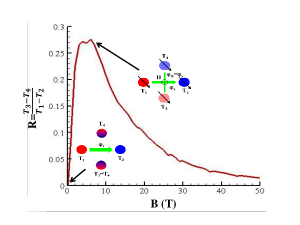
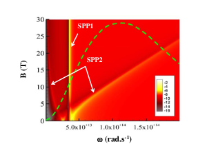
Under the action of the magnetic field, the spatial distribution of electric field radiated by the particles leads to a strongest dissipation of energy in the lower particle (particle 3) so that a Hall flux flows in the direction of positive . However, the magnitude of Hall flux is maximal for a magnetic field of about (here stands vor the unit Tesla and not for the temperature). This behavior can be understood by analyzing the resonances (localized surface modes). These modes are plotted in Fig. 15 with respect to the magnitude of the magnetic field. We clearly see the presence of three different branches (bright areas). The vertical branch is independent of the magnetic field and it corresponds to the presence of a magnetic independent surface phonon polariton (SPhP) at . The two others branches are two magneto-dependent surface modes. Contrary to the first resonance, these resonances are of plasmonic nature (see PBAHall for more details). When the magnitude of the magnetic field becomes sufficiently large, these plasmonic resonances are shifted away from the Wien’s frequency so that they do not contribute anymore to heat exchanges. On the other hand, for weak magnetic fields, these resonances give rise to supplementary channels for heat exchanges which superimpose to the channel associated with the SPhP. Moreover, the contribution of the high frequency plasmonic channel becomes more and more important as its frequency brings closer from the Wien’s frequency. The optimal transfer occurs for a magnetic field of magnitude . This situation corresponds precisely to the condition where the Hall effect is maximal.
VI Conclusion
In this paper we have summarized the very recent advances made in optics to manipulate, amplify and even store the thermal energy with the thermal photons exchanged through various many-body systems. We have demonstrated the feasability for contactless thermal analogs of transistors, volatile memories and logic gates. These devices allow for a management of heat flows either at macroscale (far-field exchanges) or at subwavelength scales (near-field exchanges) in complex architectures. Beside these building blocks for “thermotronics” we have introduced the basic theoretical framework for “magneto-thermo-plasmonics” which allows for controlling actively the heat flows in complex plasmonic networks using an external magnetic field. These results could find broad applications in MEMS/NEMS technologies, to generate mechanical work by using microresonators coupled to a transistor as well as in energy storage technology, for instance, to store and release thermal energy upon request. They could also be used to develop purely thermal wireless sensors which work by implementing logic functions with heat instead of electricity. Further analysis of the performance of such devices taking the temperature distribution inside the different parts of the system into account as shown in Ref. MessinaEtAl2016 is now in reach.
Beyond these practical applications, the physics involved in strongly correlated many-body systems is very rich. Their study has revealed the presence of various singular behaviours. Hence, we have seen that these systems can be multistable, they can locally display negative differential resistances or, in the particular case of magneto-optic systems, they can transport a photon thermal Hall flux in presence of a magnetic field. Physics of many-body systems remains largely unexplored and there is no doubt that future research in this area will reserve surprises.
References
- (1) F. Braun, Annalen der Physik und Chemie, 153, 556 (1874).
- (2) J. Bardeen and W. H. Brattain, Phys. Rev. 74, 230 (1948).
- (3) N. Tesla, L. I Anderson, Nikola Tesla: Guided Weapons and Computer Technology, Twenty First Century Books (1998).
- (4) B. Li and L. Wang and G. Casati, Appl. Phys. Lett. 88, 143501 (2006).
- (5) L. Wang, B. Li, Phys. Rev. Lett. 99, 177208 (2007).
- (6) L. Wang and B. Li, Phys. Rev. Lett. 101, 267203 (2008).
- (7) N. Li, J. Ren, L. Wang G. Zhang, P. Hänggi, and B. Li, Rev. Mod. Phys. 84, 1045 (2012).
- (8) B. Li, L. Wand and G. Casati, Phys.Rev. Lett. 93, 184301 (2004).
- (9) C. W. Chang, Okawa D., Majumdar A., and A. Zettl, Science 314, 1121 (2006).
- (10) C. Starr, J. Appl. Phys. 7, 15 (1936).
- (11) N. A. Roberts and D. G. Walker, Int. J. thermal Sciences 50, 648 (2011).
- (12) C. R. Otey, W. T. Lau, and S. Fan, Phys. Rev. Lett. 104, 154301 (2010).
- (13) S. Basu and M. Francoeur, Appl. Phys. Lett. 98, 113106 (2011).
- (14) E. Nefzaoui, J. Drevillon, Y. Ezzahri, and K. Joulain, Applied Optics, 53, 16, 3479 (2014) see also E. Nefzaoui, K. Joulain, J. Drevillon, Y. Ezzahri, Appl. Phys. Lett. 104 , 103905 (2014).
- (15) L. P. Wang and Z.M. Zhang, Nanoscale and Microscale Thermophysical Engineering, 17, 337 (2013).
- (16) J. G. Huang, Q. Li, Z. H. Zheng and Y. M. Xuan, Int. J. Heat and Mass Trans., 67, 575 (2013).
- (17) Z. Chen, C. Wong, S. Lubner, S. Yee, J. Miller, W. Jang, C. Hardin, A. Fong, J. E. Garay and C. Dames, Nature Comm., 5, 5446 (2014).
- (18) L. Zhu, C. R. Otey, and S. Fan, Phys. Rev. B 88, 184301 (2013).
- (19) P. Ben-Abdallah and S.-A. Biehs, Appl. Phys. Lett. 103, 191907 (2013).
- (20) K. Ito, K. Nishikawa, H. Lizuka and H. Toshiyoshi, Appl. Phys. Lett. 105, 253503 (2014).
- (21) P. van Zwol, K. Joulain, P. Ben-Abdallah, and J. Chevrier, Phys. Rev. B, 84, 161413(R) (2011).
- (22) P. Ben-Abdallah and S.-A. Biehs, Phys.Rev. Lett. 112, 044301 (2014).
- (23) K. Joulain, Y. Ezzahri, J. Drevillon and P. Ben-Abdallah, Appl. Phys. Lett.106, 133505 (2015).
- (24) M. M. Qazilbash, M. Brehm, B. G. Chae, P.-C. Ho, G. O. Andreev, B. J. Kim, S. J. Yun, A. V. Balatsky, M. B. Maple, F. Keilmann, H. T. Kim, and D. N. Basov, Science 318, 5857, 1750-1753 (2007).
- (25) A. S. Barker, H. W. Verleur, and H. J. Guggenheim, Phys. Rev. Lett. 17, 1286 (1966).
- (26) P. van Zwol, K. Joulain, P. Ben-Abdallah, J. J. Greffet, and J. Chevrier, Phys. Rev. B (R), 83, 20, 201404 (2011).
- (27) P. J. van Zwol, L. Ranno, and J. Chevrier, Phys. Rev. Lett. 108, 234301 (2012).
- (28) R. Messina, M. Antezza and P. Ben-Abdallah, Phys. Rev. Lett. 109, 244302 (2012).
- (29) R. Messina and Mauro Antezza, Phys. Rev. A 89, 052104 (2014).
- (30) M. Tschikin, S.-A. Biehs, P. Ben-Abdallah, F. S. S. Rosa, Eur. Phys. J. B 85, 233 (2012).
- (31) S. A. Dyakov, J. Dai, M. Yan, and M. Qiu, Phys. Rev. B 90, 045414 (2014).
- (32) J. Ordonez-Miranda, Y. Ezzahri, J. Drevillon, and K. Joulain, J. Appl. Phys. 119, 203105 (2016).
- (33) M. Kats, R. Blanchard, S. Zhang, P. Genevet, C. Ko, S. Ramanathan and F. Capasso, Phys. Rev. X 3, 041004 (2013).
- (34) L. Zhu, C. R. Otey, and S. Fan, Appl. Phys. Lett. 100, 044104 (2012).
- (35) V. Kubytskyi, S.-A. Biehs and P. Ben-Abdallah, Phys. Rev. Lett. 113, 074301 (2014).
- (36) S.M. Rytov, Y. A. Kravtsov and V. I. Tatarskii, Principles of Statistical Radiophysics, Vol. 3, (Academy of Sciences of USSR, Moscow, 1953).
- (37) D. Polder and M. Van Hove, Phys. Rev. B 4, 3303 (1971).
- (38) S.A. Dyakov, J. Dai, M. Yan, M. Qiu, J.of Phys. D: Applied Physics 48 (30), 305104 (2015).
- (39) P. Ben-Abdallah and S.-A. Biehs, arXiv:1608.01791 (2016).
- (40) M. L. Brongersma, J. W. Hartman and H. A. Atwater, Phys. Rev. B 62, R16356 (2000).
- (41) P. Ben-Abdallah, Appl. Phys. Lett. 89, 113117 (2006).
- (42) P. Ben-Abdallah, K. Joulain, J. Drevillon, and C.Le Goff, Phys. Rev. B 77, 075417 (2008).
- (43) J. Ordonez-Miranda, L. Tranchant, K. Joulain, Y. Ezzahri, J. Drevillon, and S. Volz, Phys. Rev. B 93 035428 (2016).
- (44) P. Ben-Abdallah, Phys. Rev. Lett. 116, 084301 (2016).
- (45) E. Hall, Am. J. Math. 2, 287 (1879).
- (46) M.A. Leduc, J. Phys. 2e série 6, 378 (1887).
- (47) C. Strohm, G. L. J. A. Rikken, and P. Wyder, Phys. Rev. Lett. 95, 155901 (2005).
- (48) H. Jin, O.D. Restrepo, N. Antolin, S. R. Boona, W. Windl, R. C. Myers and J. P. Heremans, Nature Mat. 14, 601–606 (2015).
- (49) M. Hirschberger et al. Phys. Rev. Lett. 115, 106603 (2015).
- (50) S. Fujimoto, Phys. Rev. Lett. 103, 047203 (2009).
- (51) H. Katsura, N. Nagaosa, and P. A. Lee, Phys. Rev. Lett. 104, 066403 (2010).
- (52) Y. Onose, T. Ideue, H. Katsura, Y. Shiomi, N. Nagaosa, and Y. Tokura, Science 329, 297 (2010).
- (53) P. Ben-Abdallah, S.-A. Biehs, and K. Joulain, Phys. Rev. Lett. 107, 114301 (2011).
- (54) R. Messina, M. Tschikin, S.-A. Biehs, and P. Ben-Abdallah, Phys. Rev. B 88, 104307 (2013).
- (55) P. Ben-Abdallah, R. Messina, S.-A. Biehs, M. Tschikin, K. Joulain, and C. Henkel, Phys. Rev. Lett. 111, 174301 (2013).
- (56) M. Nikbakht, J. Appl. Phys. 116 094307 (2014).
- (57) R. Incardone, T. Emig, and M. Krüger, EPL 106, 41001 (2014).
- (58) S. Albaladejo, R. Gómez-Medina, L. S. Froufe-Pérez, H. Marinchio, R. Carminati, J. F. Torrado, G. Armelles, A. García-Martín, and J. J. Sáenz, Optics Express, 18, 4, pp. 3556-3567 (2010).
- (59) E. D. Palik, R. Kaplan, R. W. Gammon, H. Kaplan, R. F. Wallis and J. J. Quinn, Phys. Rev. B 13, 2497 (1976).
- (60) E. Moncada-Villa, V. Fernández-Hurtado, F.J. García-Vidal, A. García-Martín and J.C. Cuevas, Phys. Rev. B, 92, 125418, (2015).
- (61) R. Messina, W. Jin, and A. W. Rodriguez, Phys. Rev. B 94, 121410(R) (2016).