Present address: ]Department of Electrical and Electronic Engineering, School of Engineering, Tokyo Institute of Technology, 4259 Nagatsuta-cho, Midori-ku, Yokohama, Kanagawa 226-8502, Japan.
Artificial control of the bias-voltage dependence of tunnelling anisotropic magnetoresistance using quantization in a single-crystal ferromagnet
Abstract
A major issue in the development of spintronic memory devices is the reduction of the power consumption for the magnetization reversal. For this purpose, the artificial control of the magnetic anisotropy of ferromagnetic materials is of great importance. Here, we demonstrate the control of the carrier-energy dependence of the magnetic anisotropy of the density of states (DOS) using the quantum size effect in a single-crystal ferromagnetic material, GaMnAs. We show that the mainly two-fold symmetry of the magnetic anisotropy of DOS, which is attributed to the impurity band, is changed to a four-fold symmetry by enhancing the quantum size effect in the valence band of the GaMnAs quantum wells. By combination with the gate-electric field control technique, our concept of the usage of the quantum size effect for the control of the magnetism will pave the way for the ultra-low-power manipulation of magnetization in future spintronic devices.
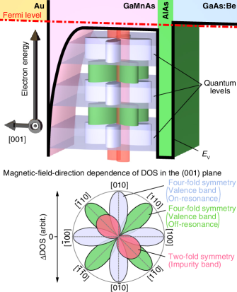
The control of the magnetic anisotropy Weisheit2007 ; Chiba2008 ; Maruyama2009 ; Nozaki2010 ; Shiota2012 ; Nozaki2013 ; Rajanikanth2013 is a particularly crucial issue for the reduction of the power required for the magnetization reversal, which will enable the exploitation of the full potential of the spintronic memory and logic devices, such as magnetic tunnel junctions Miyazaki1995 ; Moodera1995 ; Tanaka2001 ; Yuasa2004 ; Ikeda2010 and spin transistors Datta1990 ; Sugahara2004 , which may outperform the CMOS circuits commonly used in existing computers. Meanwhile, band engineering is a useful technique to manipulate the electronic structures of materials and heterostructures using an electric field Bardeen1948 , the quantum size effect Esaki1970 ; Tsu1973 , and modulation doping Dingle1978 ; Mimura1980 , and it is a well-established and important technology for the design of electronic devices based on semiconductors. For example, by designing quantum-well structures, we can completely control the quantized energy levels or two-dimensional sub-band structures of materials as calculated using band engineering. Although band engineering was developed mainly for semiconductor electronics, it could potentially be extended to magnetism because electron spins and their motions are coupled by spin-orbit interactions. However, this point of view of the usage of band engineering is lacking Ohno2000 ; Chiba2006 ; Sawicki2009 ; Xiu2010 ; Chiba2011 ; Shimamura2012 ; Weisheit2007 ; Chiba2008 ; Maruyama2009 ; Nozaki2010 ; Shiota2012 ; Nozaki2013 ; Rajanikanth2013 , and there are a wide variety of possibilities for band engineering to design or control magnetic materials and devices. Here, we demonstrate the artificial control of the carrier energy dependence of the magnetic anisotropy of the density of states (DOS) for the first time by designing quantum well structures consisting of a single-crystal ferromagnetic thin film and semiconductor barriers and tuning the strength of the quantum size effect. We used the prototypical ferromagnetic semiconductor GaMnAs, which has a band structure in which the energy regions of the valence band (VB) and impurity band (IB) overlap Kobayashi2014PRB . We found that the magnetic anisotropy of the DOS varies depending on the energy of the carriers, which has not been reported in any ferromagnetic materials. Furthermore, we revealed that the relative strength of the magnetic anisotropy between the VB and IB, which have four-fold and two-fold symmetries in the film plane, respectively, can be varied by controlling the strength of the quantum size effect induced in the VB (Fig. 1). These new findings suggest that band engineering provides the possibility of artificially designing magnetic anisotropy by controlling the electronic structures of magnetic materials. By combining this technique with the recently developed gate electric-field control technique of the carrier density and magnetization, our results will lead to ultra-low-power manipulation of magnetization in future spintronic devices.
Results
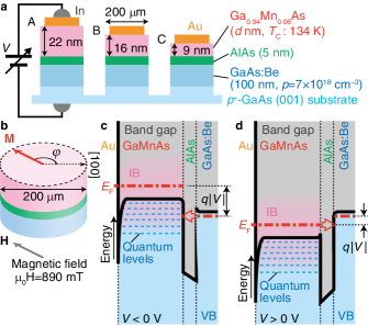
Samples. We use a tunnel heterostructure consisting of Ga0.94Mn0.06As (25 nm, Curie temperature : 134 K) / AlAs (5 nm) / GaAs:Be (100 nm, hole concentration =71018 cm-3) grown on a -GaAs (001) substrate by molecular beam epitaxy (MBE) (see Fig. 2a). We carefully etch a part of the GaMnAs layer from the surface and fabricate three tunnel-diode devices with a diameter of 200 m on the same wafer Ohya2011 ; Ohya2012 with different GaMnAs thicknesses, : 22 nm (device A), 16 nm (device B) and 9 nm (device C). In the GaMnAs layer, holes are confined by the AlAs barrier and the thin depletion layer (1 nm) formed at the surface of the GaMnAs layer Ohya2011 ; Ohya2012 , and thus, the VB energy levels in the GaMnAs layer are quantized. As shown in Fig. 2b, we measure the current-voltage (-) characteristics at 3.5 K with a strong magnetic field =890 mT applied at an angle from the direction in the plane so that the magnetization M becomes parallel to H, where is the vacuum permeability (see Supplementary Note 1 and Supplementary Figure 1 for the relation between the directions of H and M). We ground the backside of the substrate and apply a bias voltage to the Au top electrode. In this manner, we measure the magnetization-direction dependence of the tunnel conductance at various values of Gould2004 ; Saito2005 ; Ciorga2007 ; Gao2007 . For these measurements, we vary and at intervals of 2 mV and , respectively. As shown in Fig. 2c, when a negative is applied, holes tunnel from the GaAs:Be layer to the GaMnAs layer. Because is proportional to the DOS at the energy where tunnelling occurs, the energy dependence of the DOS below the Fermi level of the GaMnAs layer is detected in negative . When is positive, holes tunnel from the GaMnAs layer to the GaAs:Be layer, and thus, is proportional to the DOS at of GaMnAs regardless of (see Fig. 2d). Our measurements provide the dependence of the DOS at various energies below in GaMnAs.
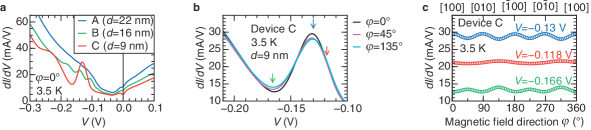
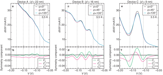
Analysis. The - characteristics obtained for devices A-C at show different oscillatory behaviour (see Fig. 3a); the oscillation becomes stronger as decreases. Also, the values of the peaks systematically change by changing , indicating that these oscillations originate from the resonant tunnelling effect Esaki1966 ; Grobis2005 induced by the quantum size effect in the VB of the GaMnAs layer Ohya2007 ; Ohya2010 ; Ohya2011 ; Muneta2013 ; Tanaka2014 . [See Supplementary Figure 3 for the - characteristics of devices A-C. More systematic data of the - characteristics of tunnelling devices with various GaMnAs thicknesses ( = 7.3 nm – 23.6 nm) are described in Supplementary Note 3 and Supplementary Figure 4.] The oscillation amplitude of decreases by changing from (along ) to (along ) or (along ) (see Fig. 3b). The peak (blue arrow) value of when is larger than that when or , whereas the dip (green arrow) value of when is smaller than that when or . This feature can been seen in Fig. 3c as the opposite sign of the oscillation of as a function of between when (the peak of - in Fig. 3b) and when (the dip of - in Fig. 3b). In Fig. 3c, the symmetry of the dependence of changes depending on .
Here, we normalize using
| (1) |
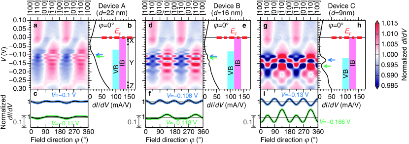
where is the value averaged over at a fixed . As seen in Fig. 4a,d,g, primarily two-fold symmetry along is observed at negative when = 22 nm, but four-fold symmetry along emerges as decreases. At the peaks and dips of the - curves indicated by the blue and green arrows in Fig. 4b,e,h, the symmetry of the - curves shown in Fig. 4c,f,i is changed from two-fold to four-fold as the resonant tunnelling is enhanced by decreasing . Because resonant tunnelling is induced in the VB, the enhanced four-fold symmetry is attributed to the VB. The curves in Fig. 4i are those obtained by normalizing the - curves shown in Fig. 3c (blue and green).
We derive the symmetry components (four-fold along ), (two-fold along ) and (two-fold along ) of the normalized - curves by fitting the following equation to the experimental normalized - curves:
| (2) |
The dependences of , and show oscillations, which synchronize with the oscillations of the - curves that are induced by the resonant tunnelling (see Fig. 5). is significantly enhanced as is decreased and the oscillation of - is enhanced. Therefore, the oscillatory behaviour of the dependence of the symmetry components is attributed to the quantization of the VB states.
We discuss the origin of the four-fold symmetry of the - curves induced by the quantum size effect in the VB of GaMnAs. Our results mean that the strength of the quantization depends on as shown in Fig. 3b, in other words, the coherence length of the VB holes depends on . In GaMnAs, there is a weak interaction between the VB holes and Mn spin magnetic moments, which indicates that the coherence length of the VB holes depends on the strength of this interaction. Thus, the four-fold symmetry of the magnetic anisotropy originates from the anisotropy of the wave function of the VB holes, which are mainly composed of As orbitals located at the lattice points having a four-fold symmetry in the film plane. This shows that the interaction between the spins and orbitals reflects the anisotropy of the wave function distribution and the direction of spins. We calculated the DOS of the VB, which is weakly interacting with the magnetic moments of Mn, using the Hamiltonian and - exchange Hamiltonian, and confirmed that the DOS vs. characteristic shows the four-fold symmetry (see Supplementary Note 4 and Supplementary Figure 5).
Magnetic anisotropy of the IB. In the region of = V – +0.1 V of the colour-coded maps shown in Fig. 4a,d,g, the normalized as a function of and is similar in devices A-C, which means that it is insensitive to the change in , and thus the two-fold symmetry along observed in this region is attributed to the IB. This insensitivity to agrees with the previous report Proselkov2012 that the magnetic anisotropy of magnetization in GaMnAs films at low temperature is independent of . In the region of V, the dependence of the normalized does not depend on because it always reflects the DOS at in GaMnAs regardless of . The two-fold symmetry along is also observed in the region of V for device A ( = 22 nm, Fig. 4a), in which the effect of the quantization of the VB holes is small. This indicates that the dependence of the tunnelling transport is dominated by the IB holes in the entire region of when the quantization of the VB holes is weak. However, as the quantization becomes stronger, the four-fold symmetry originating from the VB emerges in the IB region, which means that the IB and VB overlap (Fig. 4b,e,h). This finding is consistent with recent angle-resolved photoemission spectroscopy measurements of GaMnAs Kobayashi2014PRB .
As shown in Fig. 4b, we can classify the region of V (corresponding to the DOS below in GaMnAs) into three parts, from top to bottom: V – V (region X), V – V (region Y) and V – V (region Z). In regions X and Z, the DOS when M is along and is larger than when M is along and , whereas it is smaller in region Y. We discuss the origin of this sign change of the dependence of the DOS of the IB depending on the energy. A single Mn atom doped into GaAs forms an impurity state because of the inter-atomic interaction (hybridization) between the Mn orbitals and the As orbitals. Tang and Flatté predicted that the hybridization and spin-orbit interaction in the As orbitals result in an anti-parallel condition between the spin angular momentum of the Mn spins and the orbital angular momentum of the hole in the impurity state Tang2005 . Because of this condition, the wave function of the hole in the impurity state favours extension in the direction perpendicular to the Mn spins, and thus the distribution of the wave function depends on the direction of the Mn spins. This behaviour is well reproduced by a tight binding method (see Supplementary Note 5 and Supplementary Figure 6).
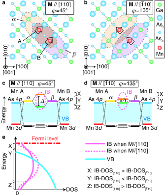
Figure 6a,b schematically illustrates the distributions of the wave functions of the two impurity states and originating from the two neighbouring Mn atoms A and B located along , respectively. Here, we consider the cases in which M is aligned in the direction (Fig. 6a) and in the direction (Fig. 6b), in which the wave functions tend to extend in the and directions, respectively (the calculated results are shown in Supplementary Figure 6). As shown in Fig. 6c,d, the hybridization between the Mn (red lines) and As (blue lines) orbitals forms (yellow line) and (purple line) around Mn atoms A and B, respectively. The bonding (green line) and anti-bonding (orange line) impurity states are formed by the wavefunction overlap between and , which is the origin of the IB Mahadevan2004PRL ; Kitchen2006 . As indicated in Fig. 6a,b, the wavefunction overlap between and is larger when M than that when M . Thus, the energy separation between the bonding and anti-bonding states when M is larger (Fig. 6c) than that when M (Fig. 6d). The energy regions X-Z indicated in Fig. 6c,d correspond to the regions of shown in Fig. 4b. When M , the anti-bonding and bonding states are formed in regions X and Z, respectively (Fig. 6c). When M , both anti-bonding and bonding states are formed in region Y (Fig. 6d). Thus, the energy dependence of the DOS of the IB differs depending on the M direction (i.e., or ), as shown in Fig. 6e. In regions X and Z, the DOS when M is larger than that when M . In region Y, the DOS when M is larger than that when M . The same scenario can be applied for the Mn atoms whose distance is larger than that between the nearest Mn atoms. The two-fold symmetry along the axis in the DOS vs. characteristic is well reproduced by a tight-binding calculation (see Supplementary Note 5 and Supplementary Figure 7).
Above, we considered only the case in which the Mn atoms are located along . Although there are several possible Mn alignments in real GaMnAs, there are reasons that only the interaction between the Mn atoms located along is important. The overlap between the wave functions of the impurity states originating from the two Mn atoms located along is known to be larger than that from the Mn atoms along other directions, such as and Mahadevan2004PRL ; Kitchen2006 . Furthermore, an anisotropic distribution of Mn atoms along in GaMnAs is predicted Birowska2012 . Slightly more Mn atoms are located along than along , which is attributed to the direction of the Mn-As bonds on the surface during the MBE growth. This is thought to be the origin of the two-fold symmetry along of the - curves. Also, the anisotropic interaction between two Mn atoms and the anisotropic distribution of the Mn atoms are thought to be the reason that GaMnAs has magnetic anisotropy with the in-plane two-fold symmetry along .
is also slightly enhanced at the peaks and dips of the resonant oscillation in - as decreases (see Fig. 5), which indicates that the VB has a small two-fold symmetry along . The two-fold symmetry of the VB is induced because the interaction between the VB holes and Mn spin magnetic moments transmits the anisotropy of the Mn distribution to the VB.
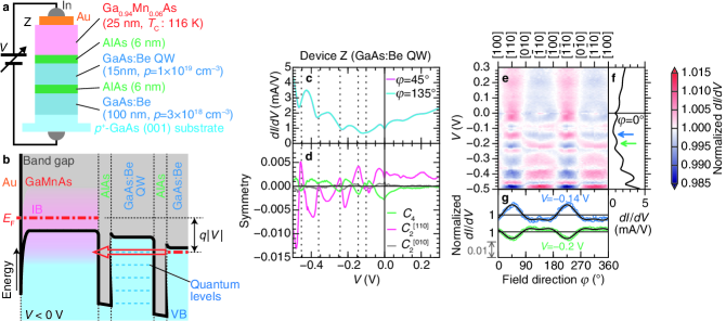
Comparison. To verify that the four-fold symmetry of the magnetic anisotropy of DOS is induced by the quantization in the GaMnAs quantum well (QW), we compare devices A-C with device Z, which consists of GaMnAs (25 nm, 116 K) / AlAs (6 nm) / GaAs:Be QW (15 nm) / AlAs (6 nm) / GaAs:Be (100 nm) grown on a -GaAs (001) substrate (see Fig. 7a,b), in which the ferromagnetic layer and the QW layer are separated and the quantum size effect does not occur in the ferromagnetic layer. The surface GaMnAs layer is thick enough to prevent the quantum size effect in this layer. We perform the same measurement on device Z. The obtained - characteristics oscillate because of the quantum size effect in the nonmagnetic GaAs:Be QW (see Fig. 7c). The dependence of the normalized - curves reflects the energy dependence of the magnetic anisotropy of the DOS of the GaMnAs electrode and exhibits an oscillatory behaviour, which is attributed to the oscillation of the - curves induced by the resonant tunnelling effect in the GaAs:Be QW (see Fig. 7c-f). Similarly to devices A-C, , and oscillate as a function of , synchronizing with the oscillation of - (Fig. 7c,d); however, the symmetry of the dependence of the normalized is mainly two-fold, reflecting the magnetic anisotropy of the GaMnAs top electrode (see Fig. 7d,e,g), which offers a remarkable contrast to the results of devices A-C that the quantum size effect in the GaMnAs QW layer enhances (four-fold symmetry). This contrast provides evidence that the magnetic anisotropy of the DOS changes by enhancing the quantum size effect in the GaMnAs QW in devices A-C. Between the different values indicated by the green and blue arrows in Fig. 7f, the symmetry of the - curves shows an opposite sign (Fig. 7g), which is induced by the small shift of the peak of the - curves (see Supplementary Note 2 and Supplementary Figure 2 for details).
It should be noted that surface states, if any, may have different anisotropy from the bulk or quantum well states. However, the surface of GaMnAs is depleted and does not induce the carrier-mediated ferromagnetism. This means that the surface does not couple with the magnetization of the GaMnAs layer beneath the surface. Thus, the DOS of the non-magnetic surface does not depend on the direction of the magnetization of the GaMnAs layer.
The magnetic anisotropy of magnetization in ferromagnetic materials reflects that of the DOS at Saito2005 . Our study indicates that the magnetic anisotropy of DOS depends on the carrier energy (applied voltage) and can be controlled by band engineering. Combining our results with the electric-field gating technique to tune the position will provide a new method to manipulate the magnetization direction by controlling the magnetic anisotropy with an ultra-low power. This method will be useful for the development of non-volatile spin devices using magnetization in the future.
Methods
Sample preparation. We grew a Ga0.94Mn0.06As (25 nm) / AlAs (5 nm) / GaAs:Be (100 nm, cm-3) tunnel heterostructure by MBE for the fabrication of devices A-C. The GaAs:Be, AlAs and GaMnAs layers were grown at 550 ∘C, 530 ∘C and 210 ∘C, respectively. We grew a Ga0.94Mn0.06As (25 nm) / AlAs (6 nm) / GaAs:Be QW (15 nm, cm-3) / AlAs (6 nm) / GaAs:Be (100 nm, cm-3) tunnel heterostructure for device Z. The GaAs:Be electrode, AlAs, GaAs:Be QW and GaMnAs layers were grown at 570 ∘C, 530 ∘C, 400 ∘C and 210 ∘C, respectively. The growth rates of GaAs, AlAs and GaMnAs were 500 nm/h.
After the growth, we annealed the samples in air at 180 ∘C for 38 h for devices A-C and 20 h for device Z to improve the crystallinity and of the GaMnAs layers Hayashi2001 ; Potashnik2001 ; Potashnik2002 ; Yu2002 ; Edmonds2002 . We estimated the of the GaMnAs layers by measuring the magnetic circular dichroism (MCD) on the samples and analysed the Arrott plots derived from the MCD- curves at various temperatures. The estimated is 134 K for devices A-C and 116 K for device Z.
We fabricated tunnel diode devices on the wafer after growth. In our process, we used chemical wet etching with an acid solution composed of phosphoric acid, hydrogen peroxide and water. For devices A-C, we sank the wafer vertically into the etching liquid so that the thickness of the GaMnAs layer changes from 0 nm to 25 nm in the same wafer. Then, we made circular mesa devices with a diameter of 200 m on the wafer by chemical wet etching for devices A-C and Z. We then coated a negative insulating resist on the wafers for the passivation of the surfaces and opened contact holes with a diameter of 180 m on the mesa devices. Then, we deposited Au on the wafers and fabricated contact pads on them.
We carried out the device process, especially the procedure from the surface etching to the Au evaporation, very quickly to minimize the oxidation of the surface GaMnAs layer. Indeed, the resonant levels systematically change with the change in the thickness of the GaMnAs layer as shown in Supplementary Figure 4. Also, similar results have been observed in tunnelling devices with GaMnAs fabricated by similar methods Ohya2011 ; Muneta2016 . Furthermore, the dependence of around 0 V and in the positive region is similar among samples A-C as shown in Fig. 4a,d,g. Therefore, extrinsic effects induced by the device process are negligible.
Data procedure. We obtained the derivative of the - characteristics numerically using the Savitzky-Golay filter. We used 7 data points to obtain the derivative at a single point.
In our fitting, we determined the fitting parameters by the modified Levenberg-Marquardt least squares method.
Acknowledgements
This work was partially supported by Grants-in-Aid for Scientific Research, including Specially Promoted Research and the Project for Developing Innovation Systems of MEXT. Part of this work was carried out under the Cooperative Research Project Program of RIEC, Tohoku University. I.M. thanks the JSPS Research Fellowship Program for Young Scientists.
Author contributions
Device fabrication and experiments: I.M., T.K.; data analysis and theory: I.M.; writing and project planning: I.M., S.O. and M.T.
Additional information
The authors declare no competing financial interests.
References
- (1) Weisheit, M. et al. Electric field-induced modification of magnetism in thin-film ferromagnets. Science 315, 349–351 (2007).
- (2) Chiba, D. et al. Magnetization vector manipulation by electric fields. Nature 455, 515–518 (2008).
- (3) Maruyama, T. et al. Large voltage-induced magnetic anisotropy change in a few atomic layers of iron. Nature Nanotech. 4, 158–161 (2009).
- (4) Nozaki, T., Shiota, Y., Shiraishi, M., Shinjo, T. & Suzuki, Y. Voltage-induced perpendicular magnetic anisotropy change in magnetic tunnel junctions. Appl. Phys. Lett. 96, 022506 (2010).
- (5) Shiota, Y. et al. Induction of coherent magnetization switching in a few atomic layers of FeCo using voltage pulses. Nature Mater. 11, 39–43 (2012).
- (6) Nozaki, T. et al. Voltage-induced magnetic anisotropy changes in an ultrathin FeB layer sandwiched between two MgO layers. Appl. Phys. Express 6, 073005 (2013).
- (7) Rajanikanth, A., Hauet, T., Montaigne, F., Mangin, S. & Andrieu, S. Magnetic anisotropy modified by electric field in V/Fe/MgO(001)/Fe epitaxial magnetic tunnel junction. Appl. Phys. Lett. 103, 062402 (2013).
- (8) Miyazaki, T. & Tezuka, N. Giant magnetic tunneling effect in Fe/Al2O3/Fe junction. J. Magn. Magn. Mater. 139, L231–L234 (1995).
- (9) Moodera, J. S., Kinder, L. R., Wong, T. M. & Meservey, R. Large magnetoresistance at room temperature in ferromagnetic thin film tunnel junctions. Phys. Rev. Lett. 74, 3273–3276 (1995).
- (10) Tanaka, M. & Higo, Y. Large tunneling magnetoresistance in GaMnAs/AlAs/GaMnAs ferromagnetic semiconductor tunnel junctions. Phys. Rev. Lett. 87, 026602 (2001).
- (11) Yuasa, S., Nagahama, T., Fukushima, A., Suzuki, Y. & Ando, K. Giant room-temperature magnetoresistance in single-crystal Fe/MgO/Fe magnetic tunnel junctions. Nature Mater. 3, 868–871 (2004).
- (12) Ikeda, S. et al. A perpendicular-anisotropy CoFeB–MgO magnetic tunnel junction. Nature Mater. 9, 721–724 (2010).
- (13) Datta, S. & Das, B. Electronic analog of the electro-optic modulator. Appl. Phys. Lett. 56, 665–667 (1990).
- (14) Sugahara, S. & Tanaka, M. A spin metal–oxide–semiconductor field-effect transistor using half-metallic-ferromagnet contacts for the source and drain. Appl. Phys. Lett. 84, 2307–2309 (2004).
- (15) Bardeen, J. & Brattain, W. H. The transistor, a semi-conductor triode. Phys. Rev. 74, 230–231 (1948).
- (16) Esaki, L. & Tsu, R. Superlattice and negative differential conductivity in semiconductors. IBM J. Res. Develop. 14, 61–65 (1970).
- (17) Tsu, R. & Esaki, L. Tunneling in a finite superlattice. Appl. Phys. Lett. 22, 562–564 (1973).
- (18) Dingle, R., Störmer, H. L., Gossard, A. C. & Wiegmann, W. Electron mobilities in modulation-doped semiconductor heterojunction superlattices. Appl. Phys. Lett. 33, 665–667 (1978).
- (19) Mimura, T., Hiyamizu, S., Fujii, T. & Nanbu, K. A new field-effect transistor with selectively doped GaAs/n-AlxGa1-xAs heterojunctions. Jpn. J. Appl. Phys. 19, L225–L227 (1980).
- (20) Ohno, H. et al. Electric-field control of ferromagnetism. Nature 408, 944–946 (2000).
- (21) Chiba, D., Matsukura, F. & Ohno, H. Electric-field control of ferromagnetism in (Ga,Mn)As. Appl. Phys. Lett. 89, 162505 (2006).
- (22) Sawicki, M. et al. Experimental probing of the interplay between ferromagnetism and localization in (Ga, Mn)As. Nature Phys. 6, 22–25 (2009).
- (23) Xiu, F. et al. Electric-field-controlled ferromagnetism in high-Curie-temperature Mn0.05Ge0.95 quantum dots. Nature Mater. 9, 337–344 (2010).
- (24) Chiba, D. et al. Electrical control of the ferromagnetic phase transition in cobalt at room temperature. Nature Mater. 10, 853–856 (2011).
- (25) Shimamura, K. et al. Electrical control of Curie temperature in cobalt using an ionic liquid film. Appl. Phys. Lett. 100, 122402 (2012).
- (26) Kobayashi, M. et al. Unveiling the impurity band induced ferromagnetism in the magnetic semiconductor (Ga,Mn)As. Phys. Rev. B 89, 205204 (2014).
- (27) Ohya, S., Takata, K. & Tanaka, M. Nearly non-magnetic valence band of the ferromagnetic semiconductor GaMnAs. Nature Phys. 7, 342–347 (2011).
- (28) Ohya, S., Muneta, I., Xin, Y., Takata, K. & Tanaka, M. Valence-band structure of ferromagnetic semiconductor (In,Ga,Mn)As. Phys. Rev. B 86, 094418 (2012).
- (29) Gould, C. et al. Tunneling anisotropic magnetoresistance: A spin-valve-like tunnel magnetoresistance using a single magnetic layer. Phys. Rev. Lett. 93, 117203 (2004).
- (30) Saito, H., Yuasa, S. & Ando, K. Origin of the tunnel anisotropic magnetoresistance in Ga1-xMnxAs/ZnSe/Ga1-xMnxAs magnetic tunnel junctions of II-VI/III-V heterostructures. Phys. Rev. Lett. 95, 086604 (2005).
- (31) Ciorga, M. et al. TAMR effect in (Ga, Mn)As-based tunnel structures. New J. Phys. 9, 351 (2007).
- (32) Gao, L. et al. Bias voltage dependence of tunneling anisotropic magnetoresistance in magnetic tunnel junctions with MgO and Al2O3 tunnel barriers. Phys. Rev. Lett. 99, 226602 (2007).
- (33) Esaki, L. & Stiles, P. J. New type of negative resistance in barrier tunneling. Phys. Rev. Lett. 16, 1108–1111 (1966).
- (34) Grobis, M., Wachowiak, A., Yamachika, R. & Crommie, M. F. Tuning negative differential resistance in a molecular film. Appl. Phys. Lett. 86, 204102 (2005).
- (35) Ohya, S., Hai, P. N., Mizuno, Y. & Tanaka, M. Quantum size effect and tunneling magnetoresistance in ferromagnetic-semiconductor quantum heterostructures. Phys. Rev. B 75, 155328 (2007).
- (36) Ohya, S., Muneta, I., Hai, P. N. & Tanaka, M. Valence-band structure of the ferromagnetic semiconductor GaMnAs studied by spin-dependent resonant tunneling spectroscopy. Phys. Rev. Lett. 104, 167204 (2010).
- (37) Muneta, I., Terada, H., Ohya, S. & Tanaka, M. Anomalous Fermi level behavior in GaMnAs at the onset of ferromagnetism. Appl. Phys. Lett. 103, 032411 (2013).
- (38) Tanaka, M., Ohya, S. & Hai, P. N. Recent progress in III-V based ferromagnetic semiconductors: Band structure, Fermi level, and tunneling transport. Appl. Phys. Rev. 1, 011102 (2014).
- (39) Proselkov, O. et al. Thickness dependent magnetic properties of (Ga,Mn)As ultrathin films. Appl. Phys. Lett. 100, 262405 (2012).
- (40) Tang, J.-M. & Flatté, M. E. Spin-orientation-dependent spatial structure of a magnetic acceptor state in a zinc-blende semiconductor. Phys. Rev. B 72, 161315 (2005).
- (41) Mahadevan, P., Zunger, A. & Sarma, D. D. Unusual directional dependence of exchange energies in GaAs diluted with Mn: Is the RKKY description relevant? Phys. Rev. Lett. 93, 177201 (2004).
- (42) Kitchen, D., Richardella, A., Tang, J.-M., Flatté, M. E. & Yazdani, A. Atom-by-atom substitution of Mn in GaAs and visualization of their hole-mediated interactions. Nature 442, 436–439 (2006).
- (43) Birowska, M., Śliwa, C., Majewski, J. A. & Dietl, T. Origin of bulk uniaxial anisotropy in zinc-blende dilute magnetic semiconductors. Phys. Rev. Lett. 108, 237203 (2012).
- (44) Hayashi, T., Hashimoto, Y., Katsumoto, S. & Iye, Y. Effect of low-temperature annealing on transport and magnetism of diluted magnetic semiconductor (Ga, Mn)As. Appl. Phys. Lett. 78, 1691–1693 (2001).
- (45) Potashnik, S. J. et al. Effects of annealing time on defect-controlled ferromagnetism in Ga1-xMnxAs. Appl. Phys. Lett. 79, 1495–1497 (2001).
- (46) Potashnik, S. J. et al. Saturated ferromagnetism and magnetization deficit in optimally annealed Ga1-xMnxAs epilayers. Phys. Rev. B 66, 012408 (2002).
- (47) Yu, K. M. et al. Effect of the location of Mn sites in ferromagnetic Ga1-xMnxAs on its Curie temperature. Phys. Rev. B 65, 201303 (2002).
- (48) Edmonds, K. W. et al. High-Curie-temperature Ga1-xMnxAs obtained by resistance-monitored annealing. Appl. Phys. Lett. 81, 4991–4993 (2002).
- (49) Muneta, I., Ohya, S., Terada, H. & Tanaka, M. Sudden restoration of the band ordering associated with the ferromagnetic phase transition in a semiconductor. Nature Commun. 7, 12013 (2016).