Electron Emission Area Depends on Electric Field and Unveils Field Emission Properties in Nanodiamond Films
Abstract
In this paper we study the effect of actual, locally resolved, field emission (FE) area on electron emission characteristics of uniform semimetallic nitrogen-incorporated ultrananocrystalline diamond ((N)UNCD) field emitters. To obtain the actual FE area, imaging experiments were carried out in a vacuum system in a parallel-plate configuration with a specialty anode phosphor screen. Electron emission micrographs were taken concurrently with - characteristics measurements. It was found that in uniform (N)UNCD films the field emitting site distribution is not uniform across the surface, and that the actual FE area depends on the applied electric field.
To quantify the actual FE area dependence on the applied electric field, a novel automated image processing algorithm was developed. The algorithm processes extensive imaging datasets and calculates emission area per image. By doing so, it was determined that the emitting area was always significantly smaller than the FE cathode surface area of 0.152 cm2 available. Namely, the actual FE area would change from % to 1.5 % of the total cathode area with the applied electric field increased.
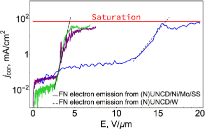
We also found that (N)UNCD samples deposited on stainless steel with molybdenum and nickel buffer layers always had better emission properties with the turn-on electric field 5 V/m and -factor of about 1,000, as compared to those deposited directly onto tungsten having the turn-on field 10 V/m and -factor of about 200. It was concluded that rough or structured surface, either on the macro- or micro- scale, is not a prerequisite for good FE properties. Raman spectroscopy suggested that increased amount of the graphitic phase, manifested as reduced D/G peak ratio, was responsible for improved emission characteristics.
Finally and most importantly, it was shown that when - curves as measured in the experiment were normalized by the field-dependent emission area, the resulting - curves demonstrated a strong kink and significant deviation from Fowler-Nordheim (FN) law, and eventually saturated at a current density of 100 mA/cm2. This value was nearly identical for all studied (N)UNCD films, regardless of the substrate.
I I. Introduction
In general, the electron field emission (FE) properties and thus efficiency of field emitters are evaluated by plotting the current density as a function of the applied electric field (linear - plot representation). For the parallel-plate electrodes configuration, is simply a product of the applied voltage over inter-electrode gap . is a product of over , where is the current measured in experiment and is the emitting surface area. The experimentally determined current density is compared to the current density predicted by the Fowler-Nordheim (FN) law that can be written in a simplified form proposed by Millikan , with , and being the work function and being the field enhancement factor, so called -factor. The FN law was originally developed to describe FE from an ideal flat metallic surface in an ultrahigh electric field 1 GV/m at 0 K 1 . In many instances, it is convenient to present properties of field emitters in vs. coordinates (so-called FN plot representation). This helps understand whether a field emitter under study obeys the FN law, as well as to calculate the -factor from the linear slope . As seen, both - plot and FN plot involve the current density rather than the apparent, as measured, current, which makes the emission area an important parameter to characterize FE properties of materials.
Conventionally, the normalization of the apparent current by the emission area is done by using the entire surface area of a field emission cathode exposed to the electric field (cathode smaller than anode) or by the entire size of an anode collecting current in the middle of a cathode (anode is smaller than cathode) 2 . This has been the standard approach for parallel-plate configuration FE measurement systems. In either of the ways of, a small cathode with the area facing a large anode or a small anode with the area collecting electrons from a part of a large cathode, is always assumed to be constant. Having constant is in contrast to locally-resolved FE characteristics of arrays and patterned/structured surfaces of semiconductors (e.g. Si and GaN) vastly reported by the groups working collaboratively at the University of Wuppertal and the Regensburg University of Applied Sciences 3 ; 4 . In those experiments, a micron-size anode was scanned across areas of interest with the gap kept constant. At each location, the applied voltage was increased or decreased (depending on the location emissivity) in order to set the emitted current to 1 nA, and 3D maps (-coordinate, -coordinate, ) were recorded. The main result was that can vary by a factor of 2 to 3 across the area of interest. These findings suggested that the emission area had to change with in experiments when the micron-size anode would be replaced with a large plate electrode. This situation can also be referred to as a problem of non-uniform (strong and weak) emitters.
Eventually, the convention of using the constant emission area: (i) makes it difficult not only to compare emission characteristics between different field emitters, but even between those of the same sample when such a sample undergoes various treatments or modifications and (ii) may lead to inadequate interpretation of experimental results. Attempts to avoid the use of and representation of field emission data by plotting the as-measured current against applied voltage is also a cumbersome approach as it has no unification between diverse experimental setups.
Similar to the mentioned locally resolved emission properties of Si and GaN emitters 3 ; 4 , there were a few reports on non-uniform emission from carbonic materials such as carbon nanotubes (CNT) 5 ; 6 and synthetic nanodiamond films 7 . Emphasis is given to these materials as CNT and synthetic polycrystalline diamond have long been acknowledged as promising FE electron sources 8 . They are efficient and simple to synthesize and scale. While exceptionally high efficiency of CNT is largely a consequence of their exceptionally high aspect ratios, nitrogen-incorporated ultrananocrystalline diamond ((N)UNCD), a highly conductive type of nanodiamond9 , is an unconventional field emitter that performs simply in planar thin film configuration and has turn-on fields 10 V/m, far below breakdown threshold for any material. Nonetheless, in Refs. 5 ; 6 ; 7 no attempts to quantify the actual FE area and to establish the dependence of the FE area on the applied electric field (if any) have been made. In this paper, we describe a novel approach to measure FE site distribution, laterally-resolved on the cathode surface, and to quantify it by obtaining the dependence of on the electric field. This approach was applied to planar thin film (N)UNCD field emitters grown on stainless steel and tungsten.

II II. Experiment
The experiments were performed in a custom imager in the parallel-plate configuration as described in Ref.10 . For convenience, the measurement setup is shown in Fig.1. The imager has a specialty anode screen which is an optically polished (1 inch dia. and 100 m thick) disk made of yttrium aluminum garnet doped with cerium (YAG:Ce) coated with a Mo film of about 7-8 nm in thickness. The distance between the sample and the anode screen is set using a micrometer holding the sample. Top and side view cameras outside the vacuum (side view camera is not depicted in Fig.1) are used to check the parallelism between the cathode and anode, and to measure the gap. A Canon DLSR camera is installed at a viewport behind the anode screen to take pictures of electron emission patterns, which are formed via cathodoluminescence (YAG:Ce has 550 nm luminescence line) when electrons, emitted from the sample and accelerated to the energy equal to the voltage applied between the electrodes, strike the YAG:Ce anode screen. Patterns of cathodoluminescence formed on the YAG:Ce anode screen placed 100 m away from the cathode represent field electron emission from the sample. The sample electrode is at ground and the anode frame is isolated and positively biased. The bias and current readings are enabled by a Keithley 2410 electrometer. Dwell time at each point to acquire simultaneously the current and voltage values with their errors, the vacuum pressure reading and a micrograph is about 5 seconds. The voltage is swept up and down with a step 1 V from 0 to 1.1 kV. Therefore, the total time per fully automated experiment is approximately 3 hours.
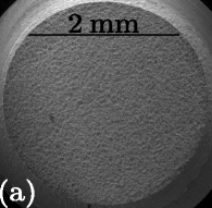
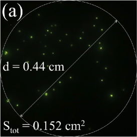
To look at the entire cathode surface area, the cathodes were purposely made smaller than the imaging Mo/YAG:Ce anode screen which is 1 inch in diameter. The anodes used were 316 stainless steel (SS) cylinder samples 4.4 mm in diameter, and tungsten cylinder sample 2.8 mm in diameter. The SS substrate cylinders were optically polished and the W cylinder substrate had macroscopic roughness (Fig.2a).
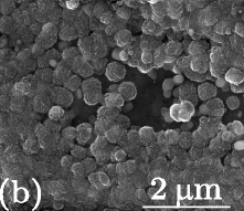
(N)UNCD films were grown using a standard procedure which was established in our previous studies using a microwave-assisted chemical vapor deposition system in a mixture of CH4/Ar/N2 with small addition of H2 for initial plasma ignition 11 ; 12 . To grow (N)UNCD on the SS substrates, Mo buffer of approximately 110 nm was deposited on SS by magnetron sputtering. Base pressure in the magnetron system was Torr. Prior to coating, the SS cylinders were cleaned in situ using RF discharge plasma. Without breaking vacuum, immediately after the cleaning, the Mo coating was deposited. Ar was used as a working gas for both cleaning and sputtering at a pressure of Torr. In addition, to vary surface morphology one Mo/SS was finished with 10 nm Ni film that was deposited in the same magnetron system. We observed that under the same growth conditions, Ni induced the (N)UNCD film to consist of densely packed spheres (Fig.2b).
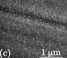
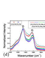
All (N)UNCD films had nearly identical topography as seen by scanning electron microscopy (SEM), i.e. they had needlelike nanostructure as illustrated in Fig.2c. Raman spectroscopy performed using a He-Ne laser (=633 nm) on the other hand revealed difference between the films on different substrates. From Fig.2d, it follows that the D/G ratio was 1.2 to 1.4 for the (N)UNCD on the SS substrates while the D/G was 1.6 for the (N)UNCD on tungsten. Smaller D/G ratio suggests higher content of graphitic phase in (N)UNCD. This behavior is consistent to the previous studies as reported in Refs.13 ; 14 ; 15 . This is also consistent with our previous measurements: an (N)UNCD film on pure Mo substrate featured a D/G=1.6 11 , while an (N)UNCD on Mo/SS had a D/G=1.3 12 . The resistivity of the (N)UNCD films is assumed to be 0.1 cm, as suggested by a four-probe measurement of a (N)UNCD film grown on an insulating Si witness coupon under the same growth conditions.
III III. Results and Discussions
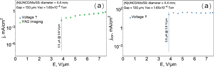
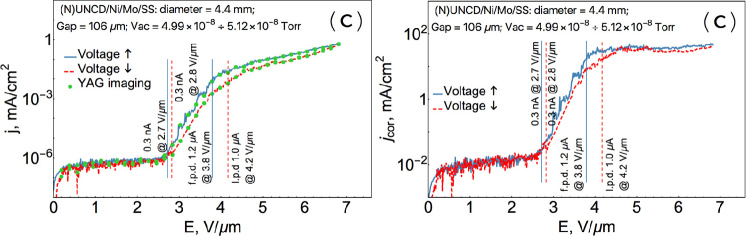
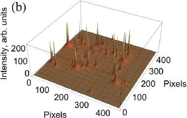
Four datasets obtained from the measurements are presented here: one from (N)UNCD/Mo/SS emitter, two sets taken at different inter-electrode gaps (147 and 106 m) from (N)UNCD/Ni/Mo/SS emitter, and one set from (N)UNCD/W emitter (we will further label the datasets as MoSS, NiMoSS1, NiMoSS2, and W, respectively). Fig.3, showing one image per dataset, illustrates emission patterns captured by the camera behind the Mo/YAG:Ce anode screen (see Fig.1) – the green light patterns are caused by the process of cathodoluminescence when field emitted electrons accelerated to a few hundred or a thousand eV bombard the phosphor. This means the patterns represent field electron emission from (N)UNCD cathode projected onto the Mo/YAG:Ce anode screen placed 100 m away from the cathode. Comparing results presented in Fig.3, our initial qualitative conclusions were that (i) the field emission site distribution in topographically uniform (N)UNCD thin films is not uniform and (ii) the (N)UNCD samples grown on the SS base would emit larger currents with emission distributed more uniformly as compared to the (N)UNCD on the W base.
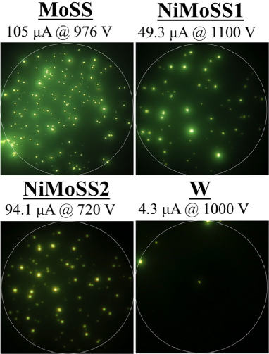
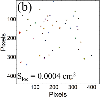
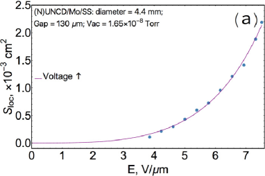
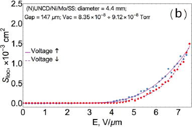
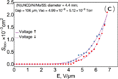
To enable accurate quantitative analysis of the extensive FE micrograph datasets described and discussed below, we made use of a clustering-based algorithm class. Such algorithms, for instance, are common tools in quantitative image analyses in astrophysics 16 and biology 17 used for accurate discrimination of a true signal from the background. The procedure in its entirety is explained in Appendix A and the core concept is mentioned in brief here. The core concept of the method is based on digitization of FE imaging micrographs and partitioning of resulting data into groups, or clusters, of similar elements. The image-clustering algorithms are adapted as required by using the strategies and approaches as described in 18 ; 19 ; 20 . The entire analysis procedure is implemented in Wolfram Mathematica to run in a parallel configuration on a multi-core computing cluster such that each processor is dedicated to work on its prescribed image. By doing so, it becomes possible to process about 100 images concurrently; reducing the total computation time dramatically. This method does not require a priori knowledge about the number and shape of clusters and can be used as an automated cathode performance test. The pixel size in cm2 is referenced to the full image size in pixels and the known diameter of the (N)UNCD cathode, 0.44 or 0.28 cm. The product of the total number of pixels combined by the clustering procedure and the pixel size in cm2 provides the total emission area per micrograph in the datasets shown in the Appendices B to E. As a specific example of how an image is converted into a pixel map of a known field emission area, we use a micrograph from the dataset MoSS, 21.8 A@650V, Appendix B. The width of the image in pixels is equal to the sample diameter , with 0.44 cm, which allows for calculating a single pixel area as small as cm2. Multiplication of the total number of selected pixels by yields the total emission area of cm2 (Fig.4).
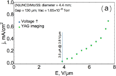
The set MoSS was measured manually starting at 3.8 V/m when reasonably bright YAG:Ce emission was detected with the camera at ISO=1,000 and a shutter speed of 1 second. After that, images were taken every 50 V until the maximum current of 100 A was reached. Therefore, there are 11 ”current-voltage-image” measurements in this case (see Appendix B).
For other samples/sets, our most recent LabVIEW software was configured such that the imaging camera took images every 20 V (sets NiMoSS1 and NiMoSS2 in Appendices C and D) and 10 V (set W, Appendix E) as voltage was first ramped up and then down. - measurements for all sets NiMoSS1, NiMoSS2 and W were performed with a step of 1 V. All image datasets (see appendices) were processed using the automated algorithm, as described is Appendix A, further to evaluate the actual FE area and determine its dependence on the electric field, .
For all four datasets in discussion, we plotted the current density versus the electric field in Fig.5 by convention, i.e. by dividing the experimentally measured current by the entire cathode area
| (1) |
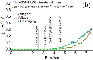
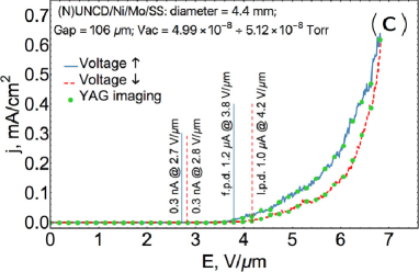
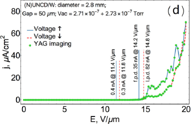

The conventional representation makes the samples seem to enable different current densities. This results in somewhat misleading interpretation of data even for the same emitter (N)UNCD/Ni/Mo/SS measured at two different gaps (panels (b) and (c) in Fig.5).
Note, in Figs.5, 7, and 8, the low field vertical markers show the turn-on electric field, i.e. the electric field at which field emission initiates. The higher field markers show the current (and the corresponding electric field) at which the image processing algorithm has detected the first pixel (first pixel detected, f.p.d., voltage ramped up) and the last pixel (last pixel detected, l.p.d., voltage ramped down) with the intensity that satisfies Eq.A4 in Appendix A. The datasets in the Appendices B to E start/end with the images before/after which the imaging processor would not detect bright pixels above the background.
After applying the imaging algorithm to the datasets shown in full in Appendices B to E, the locally resolved actual emission area was found to be a dynamic property that strongly depends on the electric field; for all the (N)UNCD field emitters measured. non-linearly but monotonically increased with the applied electric field, as illustrated in Fig.6, as well as monotonically decreased with the electric field swept down to zero following nearly identical non-linear law. The samples on the SS bases had emission area of 1% of the total cathode area (4.4 mm dia.) at the maximum output current of 100 A and electric field of about 7 V/m. The emission area of the sample on W was as small as % of the total cathode area (2.8 mm dia.) at the maximum output current of 5 A and electric field of 20 V/m.
The apparent inconsistency revealed in Fig.5 vanishes if the experimentally measured current is normalized by the dynamic surface area , which was obtained by the least square fitting of the experimental curves using a combined function
| (2) |
with . The corrected semi-log - plots are summarized in Fig.7, as well as the comparison between the conventional (left column (a-d)) normalization using and the newly proposed (right column (a-d)) normalization using is drawn. From Figs.7 and 8, it is seen that all the samples demonstrated saturation behavior. After a very short FN-like dependence manifested as a nearly linear - relation (only available for the automatically recorded datasets NiMoSS1, NiMoSS2 and W), a strong kink and deviation from the FN law took place. In fact, - still slowly increases as when plotted in linear coordinates. The lingo saturation is used because indeed saturates with , as illustrated in Fig.8, because the current increment is the same or smaller than that of .
Also note, at small voltages applied with no field emission current, . In this region, the resulting current density is infinite. To smoothly stitch the parts of the - curves before and after the turn-on field, the currents in the sets NiMoSS1, NiMoSS2, and W measured between 0 V/m and the sub-nA vertical markers identifying the turn-on field are normalized by cm2, cm2, and cm2, respectively, as obtained by the fitting at the turn-on field point. This yields current densities mA/cm2. When is calculated by the convention with , the measured current is normalized by the total cathode surface area of 0.152 cm2, or 0.062 cm2 for W dataset. This leads to a few orders of magnitude difference between and (Fig.7), and sets - curves higher against - curves in FN coordinates in Fig.8.
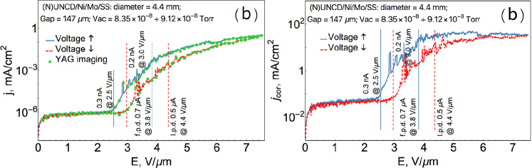

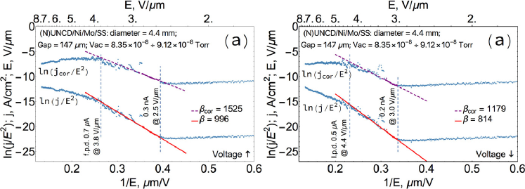
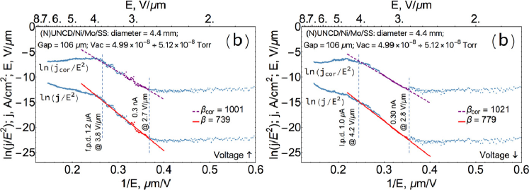
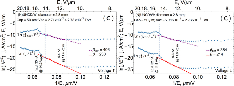
Most strikingly, it was observed that all - curves saturated at 100 mA/cm2, despite apparent significant difference was seen from - or - curves. This leads us to conclude that: (i) the saturation current level of 100 mA/cm2 represents a basic intrinsic property of (N)UNCD films while (ii) the value, i.e. the number of emitting channels available on the surface, is an effect driven by the substrate choice. The obtained results show that the deviation from the FN law onsets (kink point) when the critical current density is achieved regardless of the applied electric field. It is demonstrated that the turn-on electric field threshold and -factor, representing the FN part of the - curve, are independent from the saturation current. This is summarized in Fig.9. The sets NiMoSS1 and NiMoSS2 turned on at 2.5 V/m while the set W required the field of 11-12 V/m. This means macroscopic roughness (original roughness of the W substrate, Fig.2a) and micro- and submicroscopic topography (clustered spheres of the Ni/Mo/SS substrate, Fig.2b) are not prerequisites for good FE properties. The substrate type is a key factor under the default growth conditions in the CVD reactor. This manifests in the Raman spectra (Fig.2d) as the decreased D/G ratio, from standard 1.6 to 1.4-1.2, suggesting that emission sites and their amount depend on the graphitic fraction in the film. Similar effect was observed by other groups, see for instance Ref. 21 where the increased of amount of the graphitic phase led to improved field emission properties of (N)UNCD films as was evaluated by Raman and NEXAFS spectroscopy. The combined locally resolved field emission and Raman microscopy study must be conducted to validate this speculation.
The observed saturation effect places (N)UNCD together with the rest of conventional semiconductors, in which identical effects were reported as early as 1960’s 22 ; 23 . It has been consistently measured until this very day that, in contrast to metals, the FN law breaks down. When plotted in FN, -, coordinates, electric characteristics of semiconductors deviate and rapidly part down from the straight line. There are also a vast number of reports on the saturation effect in carbon-based materials 24 ; 25 ; 26 ; 27 . The nature of the saturation plateau was speculated to be due to electron tunneling through multiple barriers in diamond films 26 , or most frequently due to the space charge effect 27 ; 28 .
At the same time, in the original work on the space charge effect in field emission 29 , current densities as high as 107 A/cm2 are required to start screening the electric field. Unless extreme localization of emitting centers is assumed, no such current densities are observed in carbon-derived materials. This let us to speculate that the saturation phenomenon in amorphous carbon, polycrystalline diamond and CNT has the same fundamental origin apart from the space charge effect. Further experimental and theoretical work to explain the plateau and its value 100 mA/cm2, and investigation of this phenomenon more thoroughly is underway. The developed methodology of determining the actual emission area makes it possible to study other carbonic field emitters and therefore, e.g., to confirm or reject the hypothesis on the space-charge effect in CNT fibers 27 .
There are two other consequences of the imaging experiments that we have conducted. First, the electric characteristics plotted in FN coordinates in Fig.8 suggest a certain increase of the -factors for the - curves family because the pre-saturation region was modified after correcting with . Second, the hysteresis of - characteristics in Fig.5, which is commonly reported by many other groups (see e.g. Ref.27 ), is not caused by the hysteresis of the emission area within accuracy of our experiment and image processing as we do not observe significant hysteresis of the , when the voltage is ramped up and down as evidenced in Fig.6.
IV IV. Summary
An image processing concept and methodology were developed and implemented, in order to extract the actual, locally resolved, effective emission area of (N)UNCD films from emission pattern micrographs acquired using a field emission projection microscope, concurrently with current-voltage characteristics. It was shown that the effective emission area depends non-linearly on the applied electric field and repeatedly increases/decreases as the field is ramped up/down.
By normalizing the measured current by the dynamic emission area rather than by the constant entire cathode area and analyzing the resulting - curves, a few important conclusions were made: (i) semi-metallic (N)UNCD saturates similarly as semiconductors; (ii) in topographically uniform (N)UNCD thin films, field emission is not uniform; (iii) field emission current density is limited at 100 mA/cm2; this is specific to (N)UNCD, regardless of substrate; (iv) roughness and topography are not prerequisites for good FE properties.
Additionally, the proposed concept of microscopy and image processing has potential as a novel express technological procedure to accurately quantify effects in as-synthesized emitters and upon their surface termination/functionalization.
Acknowledgments. The authors would like to thank Dr Igor Volkov (GWU) for his help with implementation of the clustering algorithm and Dr. George Younes (GWU) for valuable discussions.
Euclid TechLabs was supported by the Office of Nuclear Physics of DOE through a Small Business Innovative Research grant #DE-SC 0013145.
Samples synthesis, SEM and Raman measurements were conducted in the Center for Nanoscale Materials at Argonne National Laboratory. Use of the Center for Nanoscale Materials, an Office of Science user facility, was supported by the U.S. Department of Energy, Office of Science, Office of Basic Energy Sciences, under Contract No. DE-AC02-06CH11357.
S.S. Baturin was supported by NSF grants #PHY-1535639 and #PHY-1549132 during the time of preparing the manuscript for publication.
References
- (1) R.H. Fowler and L. Nordheim, Proc. Royal Soc. A 119, 173 (1928).
- (2) P. Serbun, A systematic investigation of carbon, metallic and semiconductor nanostructures for field-emission cathode applications, Ph.D. thesis, University of Wuppertal (2014).
- (3) P. Serbun, B. Bornmann, A. Navitski, G. M ller, C. Prommesberger, C. Langer, F. Dams, and R. Schreiner, J. Vac. Sci. Technol. B 31, 02B101 (2013).
- (4) R. Schreiner, C. Langer, C. Prommesberger, S. Mingels, P. Serbun, and G. Muller, IEEE Proc. doi:10.1109/IVNC.2013.6624721 (2013).
- (5) D. Lysenkov and G. Muller, International J. Nanotechnology 2, 239 (2005).
- (6) A.G. Kolosko, E.O. Popov, S.V. Filippov, and P.A. Romanov, J. Vac. Sci. Technol. B 33, 03C104 (2015).
- (7) S. A. Lyashenko, A. P. Volkov, R. R. Ismagilov, and A. N. Obraztsov, Tech. Phys. Lett. 35, 249 (2009).
- (8) M.L. Terranova, S. Orlanducci, M. Rossi, and E. Tamburri, Nanoscale 7, 5094 (2015).
- (9) A.V. Sumant, O. Auciello, R.W. Carpick, S. Srinivasan, and J.E. Butler, MRS Bull. 35, 281 (2011).
- (10) S.S. Baturin and S.V. Baryshev, Rev. Sci. Instrum. 88, 033701 (2017).
- (11) K.J. Pérez Quintero, S. Antipov, A.V. Sumant, C. Jing, and S.V. Baryshev, Appl. Phys. Lett. 105, 123103 (2014).
- (12) S.V. Baryshev, S. Antipov, J. Shao, C. Jing, K.J. P rez Quintero, J. Qiu, W. Liu, W. Gai, A.D. Kanareykin, and A.V. Sumant, Appl. Phys. Lett. 105, 203505 (2014).
- (13) J. Birrell, J.E. Gerbi, O. Auciello, J.M. Gibson, J. Johnson, and J.A. Carlisle, Diamond Relat. Mater. 14, 86 (2005).
- (14) C.-C. Teng, S.-M. Song, C.-M. Sung, and C.-T. Lin, J. Nanomaterials 2009, 621208 (2009).
- (15) F. Klauser, D. Steinm ller-Nethl, R. Kaindl, E. Bertel, and N. Memmel, Chemical Vapor Deposition 16, 127 (2010).
- (16) F.P. Gavriil, V.M. Kaspi, and P.M. Woods, Astrophys. J. 607, 959 (2004).
- (17) P.-K. Chan, S.-H. Cheng, and T.-C. Poon, J. Electronic Imaging 16, 043003 (2007).
- (18) A. Khotanzad and A. Bouarfa, Pattern Recognition 23, 961 (1990).
- (19) A.F. Zepka, J.M. Cordes, and I. Wasserman, Astrophys. J. 427, 438 (1994).
- (20) A. Rodriguez and A. Laio, Science 344, 1492 (2014).
- (21) K.J. Sankaran, J. Kurian, H.C. Chen, C.L. Dong, C.Y. Lee, N.H. Tai, and I.N. Lin, J. Phys. D 45, 365303 (2012).
- (22) J.R. Arthur, J. Appl. Phys. 36, 3221 (1965).
- (23) L.M. Baskin, O.I. Lvov, and G.N. Fursey, Phys. Status Solidi B 47, 49 (1971).
- (24) D. Varshney, C. Venkateswara Rao, M. J. F. Guinel, Y. Ishikawa, B. R. Weiner, and G. Morell, J. Appl. Phys. 110, 044324 (2011).
- (25) C. Ducati, E. Barborini, P. Piseri, P. Milani, and J. Robertson, J. Appl. Phys. 92, 5482 (2002).
- (26) M. Liao, Z. Zhang, W. Wang, and K. Liao, J. Appl. Phys. 84, 1081 (1998).
- (27) M. Cahay, P.T. Murray, T.C. Back, S. Fairchild, J. Boeckl, J. Bulmer, K.K.K. Koziol, G. Gruen, M. Sparkes, F. Orozco, and W. O’Neill, Appl. Phys. Lett. 105, 173107 (2014).
- (28) N.S. Xu, J. Chen, and S.Z. Deng, Appl. Phys. Lett. 76, 2463 (2000).
- (29) J.P. Barbour, W.W. Dolan, J.K. Trolan, E.E. Martin, and W.P. Dyke, Phys. Rev. 92, 45 (1953).
Appendix A. The automated image processing algorithm used to process all datasets of the field emission pattern micrographs.
The routine consists of the data preprocessing, local maxima search, clustering, and segmentation. The implementation of each of the steps is described as follows.
IV.1 A1. Data Preprocessing
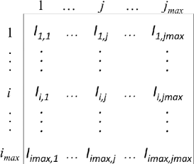
The first step towards the image processing is data preparation. The input data is an actual RGB micrograph as shown in Fig.A1. Built-in Mathematica functions, namely ColorConvert and ImageData, are used to convert RGB images into grayscale, represented in shades of gray between 0 (black) and 1 (white), and to retrieve the obtained image data in the form of a 2D array of pixel values (intensities), respectively. The intensity is represented by with , and , where and stand for the image dimensions measured in pixels as shown in Fig.A2 (typically, our images are pixels in size). As we employ Poisson distribution for image processing, we can further convert intensities into a 2D array of integer numbers . To achieve this, each value in the dataset is subtracted by the minimal intensity determined as and divided by the minimal intensity difference in the array determined as .
| (A1) |

IV.2 A2. Local Maxima Search
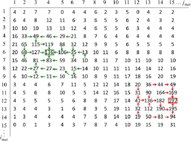
Here we use the idea that the local maximum is defined as a pixel with an intensity larger than that of any other neighbor and located at a relatively large distance from pixels with higher intensities 20 . The local maxima search routine involves calculating the distance to the nearest pixel with higher intensity. The distance is assumed to be the Euclidian distance between two pixels and with coordinates and , respectively
| (A2) |
with and running over 1 to , and and running over 1 to . This procedure is accomplished for each pixel by examining the intensities of all neighbor pixels, which lie inside the circle of radius centered at the particular pixel. In our case, for a pixel array, we use . To illustrate the general approach, let us consider a small part of a dataset. Fig.A3 illustrates the closest brighter pixel search in a pixel array. For most pixels, the nearest brighter pixels will lie at a distance . For example, Fig.A3a shows the closest brighter pixel search for the pixel , where we highlight in green the search area. It can be seen that the closest brighter pixel is located at , whereas pixel does not have any brighter pixels in the highlighted neighborhood (Fig.A3b). We define such pixels as the brightest in the neighborhood. Next, for each of the brightest in the neighborhood pixels, we calculate the distance to the closest brighter pixel in the list of the brightest pixels. For the pixel with highest intensity (global maximum), we take the distance to the closest pixel in the list of the brightest pixels. At the end of this routine, each pixel of a 2D array is associated with its own intensity and distance to the nearest brightest pixel .
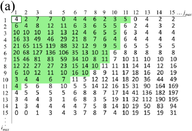
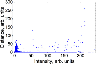
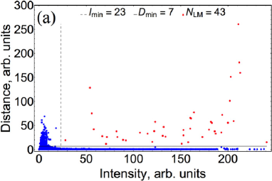
It is convenient to plot the distance as a function of intensity for each pixel. We will further call this representation the decision plot as defined by Rodriguez and Laio 20 . Fig.A4 shows the decision plot for the image in Fig.A1a. It can be seen that only some of the pixels possess a combination of high intensity and a distance much larger than . These are local maxima.
In order to completely automate the local maxima search, we need to define two parameters, the minimal distance and the minimal intensity . The pixel, which possesses these values, will be classified as a local maximum. The choice of primarily depends on the image resolution. Images with higher resolution will require a larger value of this parameter. It was found that for pixel image, = 7 is an appropriate choice, whereas the choice of requires an estimation of the background level.
Each pixel intensity is a sum of both the true signal, the light emission from a discrete emission site, the background, the emission from other emission sites, and the noise contributed by the light detection system itself. One common method of separating the signal from the background is based on an assumption that the background follows a Poisson distribution 16 ; 19 . The probability of observing a pixel with a random intensity , when the mean intensity is , can be written as
| (A3) |
Pixels that satisfy the condition
| (A4) |
where is the total number of pixels, are assumed to be the meaningful signal and are subject to further examination 16 . Since there are several emission sites on the picture, each with a different brightness, the background level can be overestimated. Therefore, pixels that satisfy the above condition are removed from the dataset and the procedure is repeated until there are no additional pixels of interest. The background level is then determined by the largest element of a final data list. The histogram in Fig.A5 illustrates an automatically determined background level. Pixels with and are local maxima and are marked in red on the decision plot (Fig.A6).

IV.3 A3. Clustering
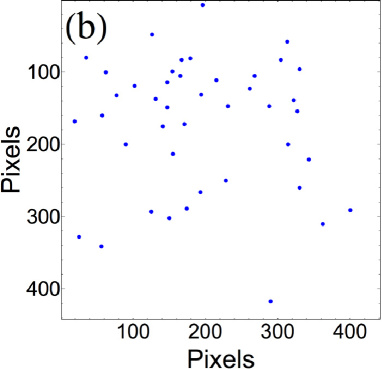
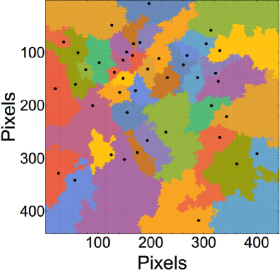
The methodology described above determines the number of local maxima, i.e. the number of seeding centers around which clusters will be built. The clustering procedure is performed by linking the pixels around the local maxima together. For each local maximum, the algorithm seeks the pixels for which this particular local maximum is a brighter pixel and attaches these pixels to the local maximum. Attached pixels, in turn, have pixels for which they are brighter neighbors (Fig.A7). The procedure is repeated for each local maximum until no more corresponding pixels are found. At this point, clusters are complete. An example of a pixel independent cluster family is shown in Fig.A8. Independent clusters around local maxima are color-coded.
IV.4 A4. Segmentation
After clusters are formed around each local maximum, we perform a segmentation procedure to decide how many pixels belong to each emission site and therefore to evaluate the total emission area at a given electric field. In order to estimate a local background, we assume that each emission site has a Gaussian shape and use a 2D Gaussian function to fit each peak
| (A5) |
Here coefficients and are the amplitude and local background, respectively, and define the pixel position of a local maximum, and and are the standard deviations in perpendicular directions (Fig.A9).
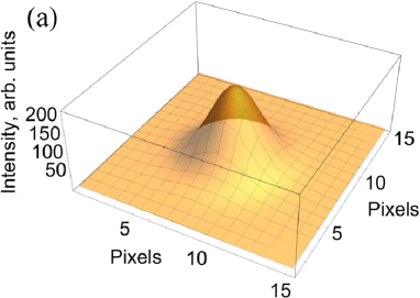
Further, we select only the pixels with intensity within one standard deviation away from the mean, which means that only the pixels that exceed the threshold
| (A6) |
contribute to the emission area. Here is the local maximum intensity and is the local background (see Fig.A10).

The pixel size in cm2 is referenced to the full image size in pixels and the known diameter of the (N)UNCD cathode, 0.44 or 0.28 cm. The product of the total number of pixels combined by the clustering procedure and the pixel size in cm2 provides the total emission area per micrograph in the datasets shown in the Appendices B to E.
Appendix B. The micrograph set for (N)UNCD/Mo/SS measured at an inter-electrode gap (UNCD-YAG) of 130 m and pressure Torr. All 11 images were acquired in the course of ramping the voltage up.
![[Uncaptioned image]](/html/1703.04033/assets/x39.png)
Appendix C. The micrograph set for (N)UNCD/Ni/Mo/SS measured at an inter-electrode gap (UNCD-YAG) of 147 m and pressure about Torr. The presented 51 images are those on which the image processing algorithm has detected high intensity pixels above the background threshold. The full set was recorded in the course of ramping the voltage up (0 to 1,100 V with a step of 20 V) and then down (1,100 to 0 V with a step of 20 V).
![[Uncaptioned image]](/html/1703.04033/assets/x40.png)
![[Uncaptioned image]](/html/1703.04033/assets/x41.png)
Appendix D. The micrograph set for (N)UNCD/Ni/Mo/SS measured at an inter-electrode gap (UNCD-YAG) of 106 m and pressure about Torr. The presented 30 images are those on which the image processing algorithm has detected high intensity pixels above the background threshold. The full set was recorded in the course of ramping the voltage up (0 to 720 V with a step of 20 V) and then down (720 to 0 V with a step of 20 V).
![[Uncaptioned image]](/html/1703.04033/assets/x42.png)
Appendix E. The micrograph set for (N)UNCD/W measured at an inter-electrode gap (UNCD-YAG) of 50 m and pressure about Torr. The presented 56 images are those on which the image processing algorithm has detected high intensity pixels above the threshold. The full set was recorded in the course of ramping the voltage up (0 to 1,000 V with a step of 10 V) and then down (1,000 to 0 V with a step of 10 V).
![[Uncaptioned image]](/html/1703.04033/assets/x43.png)
![[Uncaptioned image]](/html/1703.04033/assets/x44.png)