All-optical switching and unidirectional plasmon launching with electron-hole plasma driven silicon nanoantennas
Abstract
High-index dielectric nanoparticles have become a powerful platform for modern light science, enabling various fascinating applications, especially in nonlinear nanophotonics for which they enable special types of optical nonlinearity, such as electron-hole plasma photoexcitation, which are not inherent to plasmonic nanostructures. Here, we propose a novel geometry for highly tunable all-dielectric nanoantennas, consisting of a chain of silicon nanoparticles excited by an electric dipole source, which allows tuning their radiation properties via electron-hole plasma photoexcitation. We show that the slowly guided modes determining the Van Hove singularity of the nanoantenna are very sensitive to the nanoparticle permittivity, opening up the ability to utilize this effect for efficient all-optical modulation. We show that by pumping several boundary nanoparticles with relatively low intensities may cause dramatic variations in the nanoantenna radiation power patterns and Purcell factor. We also demonstrate that ultrafast pumping of the designed nanoantenna allows unidirectional launching of surface plasmon-polaritons, with interesting implications for modern nonlinear nanophotonics.
I Introduction
In the last several years high-index dielectric nanoparticles and nanostructures Kuznetsov et al. (2016); Krasnok et al. (2012); Jahani and Jacob (2016) proved to be a promising platform for various nanophotonic applications, in particular for the design of functional nanoantennas Rolly et al. (2013); Krasnok et al. (2014); Li et al. (2015), enhanced spontaneous emission Regmi et al. (2016); Krasnok et al. (2015a); Bouchet et al. (2016); Sun et al. (2016), photovoltaics Brongersma et al. (2014), frequency conversion Carletti et al. (2015); Makarov et al. (2016); Shorokhov et al. (2016), Raman scattering Dmitriev et al. (2016), and sensing Caldarola et al. (2015). The great interest in such nanostructures is caused mainly by their ability to control the electric and magnetic components of light at the nanoscale Kuznetsov et al. (2016), while exhibiting low dissipative losses inherent to the materials with a negligible concentration of free charges Caldarola et al. (2015). In particular, it has been demonstrated that nanoantennas composed of high-index nanoparticles have the ability to realize directional scattering of the incident light and to effectively transform the near field of feeding quantum sources into propagating electromagnetic waves Krasnok et al. (2012).
Modification of the spontaneous emission rate of a quantum emitter induced by its environment, known as the Purcell effect Purcell (1946); Pelton (2015), is not so pronounced in all-dielectric structures Bozhevolnyi and Khurgin (2016); Krasnok et al. (2012), as in microcavities Vahala (2003) or plasmonic nanoantennas Russell et al. (2012); Akselrod et al. (2014). This is due to the fact that optical resonances of high-index nanoparticles are characterized by relatively low quality factors and large mode volumes, which results in low efficiency of light-matter interaction. However, it was recently shown that this disadvantage can be overcome by relying on the Van Hove singularity of a chain of high-index nanoparticles Krasnok et al. (2016). Such approach allows to substantially enhance the local density of optical states (LDOS) at the location of a quantum source and thus achieve high values of the Purcell factor with relatively small dielectric nanostructures while leaving unaltered all their other advantages.
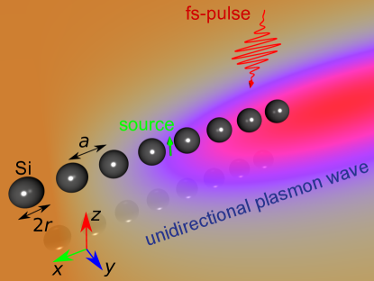
High-index dielectric nanostructures are also of a special interest for nonlinear nanophotonics, because they can exhibit strong nonlinear responses. It was recently predicted and experimentally demonstrated that photoexcitation of dense electron-hole plasma (EHP) in silicon (Si) nanoparticles Makarov et al. (2015); Shcherbakov et al. (2015); Baranov et al. (2016a) and nanodimers Baranov et al. (2016b) by femtosecond laser (fs-laser) pulses is accompanied by a dramatic modification of the radiation properties, whereas generation of EHP in germanium nanoantennas can even turn them into plasmonic ones in the mid-IR region Fischer et al. (2016). Here, we propose a highly tunable all-dielectric nanoantenna, consisting of a chain of Si nanoparticles excited by an electric dipole source, which allows for tuning its radiation properties via electron-hole plasma photoexcitation. We theoretically and numerically demonstrate the tuning of radiation power patterns and Purcell factor by pumping several boundary nanoparticles in the chain with relatively low peak intensities of fs-laser pulses. Moreover, we show that the proposed nanoantenna, being driven by fs-laser pulses, allows unidirectional launching of surface plasmon waves (Fig. 1), making this solution attractive for all-optical light manipulation systems.
II Results and discussion
To briefly recall the origin of the Van Hove singularity, let us consider a general periodic one-dimensional system supporting a set of guided modes. Decomposing its Green tensor into a series of eigenmodes, one can calculate the Purcell factor in such a system according to Ref. Manga Rao and Hughes (2007)
| (1) |
with being the effective area of the resonant guided mode, the free space wavelength, the group velocity of the mode, and is the speed of light. The divergence of the Purcell factor, occurring at the point of zero group velocity, is known as a Van Hove singularity. This expression clearly suggests that the Purcell factor benefits from slow light modes of the structure. In reality, its finite size prevents this divergence, but nevertheless largely enhanced Purcell factor can still be traced to the Van Hove singularity of the original structure.
Here, we realize a Van Hove singularity using a chain of spherical dielectric nanoparticles excited by an electric dipole (green arrow), placed in the center of the chain and perpendicularly oriented to the chain axis, Fig. 1. We choose Si particles with dielectric permittivity close to 16 in the operational frequency range Aspnes and Studna (1983). The nanoparticles have all the same radius and the center-to-center distance between neighboring particles is .
The optical properties of nanoparticle-based nanoantennas can be understood from the infinite chain modal dispersion Koenderink (2009); Alú and Engheta (2006). Therefore we start by calculating the optical properties of the infinite structure with an analytical approach, based on the well-known coupled-dipole model. Each particle is modeled as a combination of magnetic and electric dipoles with magnetic m and electric p momenta, oscillating with frequency []. In the CGS system this approach leads to the linear system of equations:
| (2) | ||||
where , , is the dyadic product, is the unit tensor, is the unit vector in the direction from -th to -th sphere, and
| (3) | ||||
where is the distance between the centers of -th and -th spheres, is the permittivity of the host medium, is the host wavenumber, , and is the frequency. The quantities and are the magnetic and electric polarizabilities of a spherical particle Bohren and Huffman (1998):
| (4) |
where and are electric and magnetic Mie coefficients. The coupled dipole approximation outlined above is justified for the geometrical parameters of the nanoparticles and their relative distance Savelev et al. (2014).
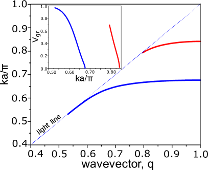
The solution of Eq. 2 without source [dispersion of waveguide eigenmodes ] for the infinite dielectric chain with nm and nm in free space is shown in Fig. 2. Here, we use the dimensionless wavenumber , where is the Bloch propagation constant. The blue and red curves correspond to transverse magnetic (TM) and transverse electric (TE) modes, respectively, which are the only modes excited by the dipole source with the chosen orientation. Both of these modes are characterized by induced magnetic and electric moments (except the points at the band edge). Due to the spectral separation of resonances of the single particle, the magnetic moments are dominant in the first branch (TM), and electric moments in the second one (TE). The inset in Fig. 2 shows the calculated group velocities of the waveguide modes as a function of frequency. It can be seen that the group velocity drops to zero at the band edge around and . Since the symmetry of the ED source matches the symmetry of the TM staggered mode (and not the TE one), we may expect significant enhancement of the Purcell factor for a finite system around the first frequency.
To confirm this expectation, we calculate the Purcell factor using the Green’s tensor approach Novotny and Hecht (2006):
| (5) |
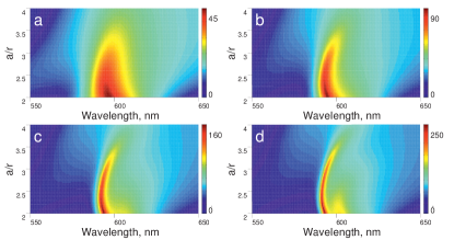
with being Green’s tensor of an electric dipole in the center of chain (point of the dipole source localization) and being the unit vector pointing in the direction (Fig. 1). Fig. 3 shows the calculated Purcell factor as a function of wavelength and ratio for a dipole source located in the center of a dielectric chain with different number of particles: (a) , (b) , (c) , and (d) . We observe that increasing the number of nanoparticles gives rise to enhancement of Purcell factor. For example, the maximal value of the Purcell factor for reaches 250. Along with the calculations shown in Fig. 2, we conclude that the maximum of Purcell factor arises around the Van Hove singularity.
Now, we are ready to show that the excitation of slow guided modes determining a Van Hove singularity is very sensitive to the electrodynamical properties of the system. Our aim is to utilize this effect to engineer highly tunable nanoantennas, for which relatively low intensities of external laser pulses can control and cause a dramatic modification of the optical properties of the material, and consequently the radiation properties (intensities of emission and power patterns) of the nanoantenna. To enable the switching of the nanoantenna properties we employ the nonlinear response caused by electron-hole plasma photoexcitation the in boundary particles of the Si nanoantenna.
To describe EHP-induced tuning of the nanoantenna, we employ the analytical approach developed in Ref. Baranov et al. (2016a). The dynamics of volume-averaged EHP density is modeled via the rate equation
| (6) |
where, are the volume-averaged absorption rates due to one- and two-photon processes, and is the EHP recombination rate which depends on EHP density Yu and Cardona (2005). The absorption rates are written in the usual form as and , where angle brackets denote averaging over the nanoparticle volume, and with being two-photon absorption coefficient. The relaxation rate of EHP in c-Si is dominated by Auger recombination with s-1cm6 (Ref. Shank et al. (1983)). Now the permittivity of photoexcited Si should be related to time-dependent EHP density:
| (7) |
where is the permittivity of non-excited material, while , , and are the contributions from bandgap renormalization, band filling, and Drude term, respectively. The detailed expressions for all contributions in Eq. (7) can be found in Ref. Baranov et al. (2016a). In total, these three contributions lead to decrease of the real part of permittivity with increasing EHP density.
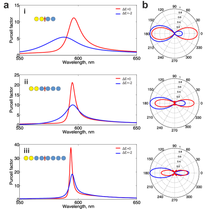
The spectral dependency of the Purcell factor before and after EHP photoexcitation are presented in Fig. 4(a) for a different number of particles . The calculations are performed for the change of the real part of Si permittivity [where ], which is achieved at the wavelength of 600 nm upon excitation of EHP with density cm-3. The decrease of the Purcell factor approximately by a factor of 2 in all cases (i–iii), along with the spectral broadening, are caused by symmetry breaking of the chain and corresponding decrease of the quality factor of the Van Hove singularity mode. The EHP photoexcitation also modifies the radiation pattern of the nanoantenna, Fig. 4(b). Before the plasma excitation () the radiation pattern has two symmetric lobes directed along the chain axis in forward and backward directions (red curves). In this case, the maximal value of directivity grows with increasing of . After the plasma excitation (), nanoantenna radiates mostly in the direction of the affected particles. We note that the degree of modification of the radiation pattern grows with increasing number of particles. For example, in the case of =8 [Fig. 4(b)iii], the directivity in the left direction is two times larger that in the right one. Thus, the EHP photoexcitation can be applied for all-optical switching of radiation patterns. Such dramatic tuning of the radiation pattern is caused by the Van Hove singularity regime of the initially unaffected nanoantenna.
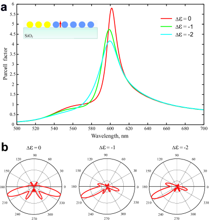
In the vast majority of nanoantenna realizations, the substrate substantially affects the nanoantenna characteristics (see, for example, Ref. Krasnok et al. (2015b)). For this reason, we analyze how a SiO2 substrate affects the nanoantenna’s characteristics. To simulate the nanoantenna consisting of 8 nanoparticles, located on the SiO2 substrate with , we utilize the commercial software CST Microwave Studio. To calculate the Purcell factor, the method based on the input impedance of a small (in terms of radiation wavelength) dipole antenna Krasnok et al. (2015c) has been applied. The corresponding results are presented in Fig. 5(a). These spectra qualitatively agree with our analytical calculations presented above. However, in this case, the substrate breaks the mirror symmetry with respect to the axis, which leads to a reduction of Purcell factor. Moreover, the numerical calculations reveal that the sharpest effect of EHP photoexcitation on the radiation pattern manifests itself when three boundary particles are illuminated [see inset in the Fig. 5(a)]. During the EHP photoexcitation, the maximum of Purcell factor slightly decreases from 5.9 to 4.7 for and to 4.1 for accompanied by shifting of the resonant frequency to the shorter wavelengths due to the decrease of boundary particles dielectric permittivity.
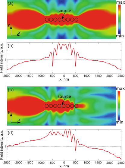
Fig. 5(b) demonstrates the change in radiation pattern induced by EHP photoexcitation for the nanoantenna on SiO2 substrate. When =0 (unaffected nanoantenna) the radiation power pattern is symmetric with respect to the dipole axis and has two main lobes. It can be observed that the mirror symmetry of the radiation patterns with respect to the axis is broken, and the main lobes are oriented into the substrate, which has higher refractive index than the upper space. The modification of three boundary particles dramatically changes the power pattern: the reconfiguration is sufficient for practical applications even for .
This effect can be used for the unidirectional launching of waveguide modes in plasmonic waveguides at will. Fig. 6 demonstrates this phenomenon, showing the calculated radiation of a nanoantenna composed of 8 Si nanoparticles placed with the period of 200 nm on a silver substrate with the 60 nm spacer glass (SiO2) layer. The SiO2 spacer serves as a buffer layer for the protection of silver substrate from sulfidation. The dipole source is located at the center of chain perpendicular to the substrate. Figs. 6(a) and (b) show the electric field distribution profile and the electric field intensity as a function of the coordinate in the cases of the unaffected nanoantenna, respectively. It can be seen that the nanoantenna launches surface plasmons symmetrically to the positive and negative directions of axis . However, when three boundary nanoparticles are illuminated by the pump beam, the nanoantenna launches surface plasmons almost unidirectionally, Figs. 6(c,d). We achieve a value of front-to-back ratio up to 5 for this geometry, Fig. 6(d).
As a final step of our analysis, we estimate the parameters of a pump pulse required for generation of cm-3 EHP, assumed in the electromagnetic calculations above. At the high intensities required for photoexcitation of Si, two-photon absorption (TPA) usually dominates over one-photon process Baranov et al. (2016a). Silicon has a particularly large TPA coefficient between 600 and 700 nm Reitze et al. (1990). We set the wavelength of pump pulse to 650 nm in order to avoid the interference between pump and dipole source signals. Estimating the enhancement factors for and for a Si nanoparticle on a substrate and using equations (6) to calculate the dynamics of EHP density, we find that a 200 fs pulse with peak intensity of 35 GW/cm2 and 25 GW/cm2 provides cm-3 EHP in the nanoparticle on a glass and silver substrates, respectively, during ps that should be sufficient for obtaining the degree of tuning demonstrated above.
III Conclusion
In conclusion, we have proposed highly tunable all-dielectric nanoantennas, consisting of a chain of Si nanoparticles excited by an electric dipole source, that allow tuning their radiation properties via electron-hole plasma photoexcitation. We have theoretically and numerically demonstrated the tuning of radiation power patterns and the Purcell effect by additional pumping several boundary nanoparticles with relatively low peak intensities. We have also demonstrated that these effects remain valid for the nanoantenna situated on a dielectric surface. The proposed nanoantenna, driven by fs-laser pulses, also allows tunable unidirectional launching of surface plasmon waves, with interesting implications for modern nonlinear nanophotonics.
Acknowledgments
This work was financially supported by Russian Science Foundation (Grant 15-19-30023) and by Russian Foundation for Basic Research (Project 16-37-60076). This work was also partially supported by the Air Force Office of Scientific Research.
References
- Kuznetsov et al. (2016) A. I. Kuznetsov, A. E. Miroshnichenko, M. L. Brongersma, Y. S. Kivshar, and B. Luk’yanchuk, Science 354, aag2472 (2016).
- Krasnok et al. (2012) A. E. Krasnok, A. E. Miroshnichenko, P. A. Belov, and Y. S. Kivshar, Optics Express 20, 20599 (2012).
- Jahani and Jacob (2016) S. Jahani and Z. Jacob, Nature Nanotechnology 11, 23 (2016).
- Rolly et al. (2013) B. Rolly, J.-M. Geffrin, R. Abdeddaim, B. Stout, and N. Bonod, Scientific Reports (2013).
- Krasnok et al. (2014) A. E. Krasnok, C. R. Simovski, P. A. Belov, and Y. S. Kivshar, Nanoscale 6, 7354 (2014).
- Li et al. (2015) S. V. Li, D. G. Baranov, A. E. Krasnok, and P. A. Belov, Applied Physics Letters 107, 171101 (2015).
- Regmi et al. (2016) R. Regmi, J. Berthelot, P. M. Winkler, M. Mivelle, J. Proust, F. Bedu, I. Ozerov, T. Begou, J. Lumeau, H. Rigneault, M. F. García-Parajó, S. Bidault, J. Wenger, and N. Bonod, Nano Letters 16, 5143 (2016).
- Krasnok et al. (2015a) A. E. Krasnok, A. Maloshtan, D. N. Chigrin, Y. S. Kivshar, and P. A. Belov, Laser & Photonics Reviews 9, 385 (2015a).
- Bouchet et al. (2016) D. Bouchet, M. Mivelle, J. Proust, B. Gallas, I. Ozerov, M. F. Garcia-Parajo, A. Gulinatti, I. Rech, Y. De Wilde, N. Bonod, V. Krachmalnicoff, and S. Bidault, Phys. Rev. Applied 6, 064016 (2016).
- Sun et al. (2016) S. Sun, L. Wu, P. Bai, and C. Png, Physical Chemistry Chemical Physics 18, 19324 (2016).
- Brongersma et al. (2014) M. L. Brongersma, Y. Cui, and S. Fan, Nature Materials 13, 451 (2014).
- Carletti et al. (2015) L. Carletti, A. Locatelli, O. Stepanenko, G. Leo, and C. De Angelis, Optics Express 23, 26544 (2015).
- Makarov et al. (2016) S. Makarov, A. Tsypkin, T. Voytova, V. Milichko, I. Mukhin, A. Yulin, S. Putilin, M. Baranov, A. Krasnok, I. Morozov, et al., Nanoscale 8, 17809 (2016).
- Shorokhov et al. (2016) A. S. Shorokhov, E. V. Melik-Gaykazyan, D. A. Smirnova, B. Hopkins, K. E. Chong, D.-Y. Choi, M. R. Shcherbakov, A. E. Miroshnichenko, D. N. Neshev, A. A. Fedyanin, and Y. S. Kivshar, Nano Letters 16, 4857 (2016).
- Dmitriev et al. (2016) P. A. Dmitriev, D. G. Baranov, V. A. Milichko, S. V. Makarov, I. S. Mukhin, A. K. Samusev, A. E. Krasnok, P. A. Belov, and Y. S. Kivshar, Nanoscale 8, 9721 (2016).
- Caldarola et al. (2015) M. Caldarola, P. Albella, E. Cortés, M. Rahmani, T. Roschuk, G. Grinblat, R. F. Oulton, A. V. Bragas, and S. A. Maier, Nature Communications 6, 7915 (2015).
- Purcell (1946) E. M. Purcell, Phys. Rev 69, 681 (1946).
- Pelton (2015) M. Pelton, Nature Photon. 9, 427 (2015).
- Bozhevolnyi and Khurgin (2016) S. I. Bozhevolnyi and J. B. Khurgin, Optica 3, 1418 (2016).
- Vahala (2003) K. J. Vahala, Nature 424, 839 (2003).
- Russell et al. (2012) K. J. Russell, T.-L. Liu, S. Cui, and E. L. Hu, Nature Photon. 6, 459 (2012).
- Akselrod et al. (2014) G. M. Akselrod, C. Argyropoulos, T. B. Hoang, C. Ciraci, C. Fang, J. Huang, D. R. Smith, and M. H. Mikkelsen, Nature Photon. 8, 835 (2014).
- Krasnok et al. (2016) A. Krasnok, S. Glybovski, M. Petrov, S. Makarov, R. Savelev, P. Belov, C. Simovski, and Y. Kivshar, Applied Physics Letters 108, 211105 (2016).
- Makarov et al. (2015) S. Makarov, S. Kudryashov, I. Mukhin, A. Mozharov, V. Milichko, A. Krasnok, and P. Belov, Nano Letters 15, 6187 (2015).
- Shcherbakov et al. (2015) M. R. Shcherbakov, P. P. Vabishchevich, A. S. Shorokhov, K. E. Chong, D.-Y. Choi, I. Staude, A. E. Miroshnichenko, D. N. Neshev, A. A. Fedyanin, and Y. S. Kivshar, Nano Letters 15, 6985 (2015).
- Baranov et al. (2016a) D. G. Baranov, S. V. Makarov, V. A. Milichko, S. I. Kudryashov, A. E. Krasnok, and P. A. Belov, ACS Photonics 3, 1546 (2016a), arXiv:1603.04397 .
- Baranov et al. (2016b) D. G. Baranov, S. V. Makarov, A. E. Krasnok, P. A. Belov, and A. Alù, Laser & Photonics Reviews 10, 1009 (2016b).
- Fischer et al. (2016) M. P. Fischer, C. Schmidt, E. Sakat, J. Stock, A. Samarelli, J. Frigerio, M. Ortolani, D. J. Paul, G. Isella, A. Leitenstorfer, P. Biagioni, and D. Brida, Phys. Rev. Lett. 117, 047401 (2016).
- Manga Rao and Hughes (2007) V. S. C. Manga Rao and S. Hughes, Physical Review B 75, 205437 (2007).
- Aspnes and Studna (1983) D. E. Aspnes and A. A. Studna, Physical Review B 27, 985 (1983).
- Koenderink (2009) A. F. Koenderink, Nano Letters 9, 4228 (2009).
- Alú and Engheta (2006) A. Alú and N. Engheta, Physical Review B 74, 205436 (2006).
- Bohren and Huffman (1998) C. F. Bohren and D. R. Huffman, Absorption and scattering of light by small particles (New York: Wiley, 1998).
- Savelev et al. (2014) R. S. Savelev, A. P. Slobozhanyuk, A. E. Miroshnichenko, Y. S. Kivshar, and P. A. Belov, Physical Review B 89, 035435 (2014).
- Novotny and Hecht (2006) L. Novotny and B. Hecht, Principles of Nano-Optics (Cambridge University Press, 2006).
- Yu and Cardona (2005) P. Yu and M. Cardona, Fundamentals of semiconductors (Springer, 2005).
- Shank et al. (1983) C. V. Shank, R. Yen, and C. Hirlimann, Phys. Rev. Lett. 50, 454 (1983).
- Krasnok et al. (2015b) A. E. Krasnok, A. Maloshtan, D. N. Chigrin, Y. S. Kivshar, and P. A. Belov, Laser & Photonics Reviews 9, 385 (2015b), arXiv:1411.1583 .
- Krasnok et al. (2015c) A. E. Krasnok, A. P. Slobozhanyuk, C. R. Simovski, S. A. Tretyakov, A. N. Poddubny, A. E. Miroshnichenko, Y. S. Kivshar, and P. A. Belov, Scientific Reports 5 (2015c).
- Reitze et al. (1990) D. H. Reitze, T. R. Zhang, W. M. Wood, and M. C. Downer, J. Opt. Soc. Am. B 7, 84 (1990).