Thickness dependent electronic structure in WTe2 thin films
Abstract
We study the electronic structure of WTe2 thin film flakes with different thickness down to 11 nm. Angle-dependent quantum oscillations reveal a crossover from a three-dimensional (3D) to a two-dimensional (2D) electronic system when the sample thickness is reduced below 26 nm. The quantum oscillations further show that the Fermi pockets get smaller as the samples are made thinner, indicating that the overlap between conduction and valence bands is getting smaller and implying the spatial confinement could lift the overlap in even thinner samples. In addition, the quadratic magnetoresistance (MR) also shows a crossover from 3D to 2D behavior as the samples are made thinner, while gating is shown to affect both the quadratic MR and the quantum oscillations of a thin sample by tuning its carrier density.
Tungsten ditelluride, one of the transition metal dichalcogenides, has attracted a lot of attention recently. Bulk WTe2 exhibits an unsaturated and extremely large magnetoresistance (MR) which could be used to design devices such as magnetic sensors Ali et al. (2014). It is believed that the magnetoresistance occurs due to the nearly equal electron and hole concentrations Ali et al. (2014); Pletikosić et al. (2014); Zhu et al. (2015); Cai et al. (2015); Xiang et al. (2015a); Zhao et al. (2015); Lv, H. Y. et al. (2015); Das et al. (2016), and forbidden backscattering due to strong spin-orbit coupling also plays an important role Jiang et al. (2015). Surprisingly, although WTe2 is a layered material, the anisotropy of the effective mass is as low as 2 at room temperature Thoutam et al. (2015). Quantum oscillations can be observed along three different crystal axes Zhu et al. (2015); Rhodes et al. (2015), which makes it close to a three-dimensional (3D) electronical system instead of two-dimensional (2D) electronic system Behnia (2015). Bulk WTe2 is also predicted to be a type-II Weyl semimetal, in which Lorenz invariance is absent and the Weyl point appears at the boundary of electron and hole pockets Soluyanov et al. (2015). This prediction has triggered renewed interests in this material Wu et al. (2016); Wang et al. (2016a); Feng et al. (2016); Sánchez-Barriga et al. (2016); Bruno et al. (2016); Wang et al. (2016b). Furthermore, monolayer WTe2 is predicted to be a nontrivial semimetal where both topological metallic edge states and 2D metallic bulk state are present Qian et al. (2014). Applying a small tensile strain, however, could lift the overlap of the conduction and valence bands and turn it into a 2D topological insulator Qian et al. (2014), where only the topological edge state is metallic Kane and Mele (2005a); *PhysRevLett.95.226801; Bernevig and Zhang (2006); *Science3141757; *Science3185851.
The studies of the unusual MR of bulk WTe2 has been extended to thin film samples Wang et al. (2015, 2016c); Na et al. (2016); Woods et al. (2016); Liu et al. (2016, 2017). Electron and hole compensation is found in samples down to thickness around 10 nm, but the MR of thin films is suppressed significantly due to surface scattering from amorphous surface oxides Na et al. (2016); Woods et al. (2016); Lee et al. (2015); Ye et al. (2016); Naylor et al. (2017). Meanwhile the carrier density also has been observed to decrease as the samples are made thinner Na et al. (2016); Woods et al. (2016), which is unexpected if it is assumed that thin film samples are simply thinner cases of 3D bulk samples. Recently optical and transport measurements in thin film samples with thickness from 9 to 11.7 nm suggests a band gap could open in monolayer sample and this is supported by band structure calculations Zheng et al. (2016). Another study reported that semi-metallic monolayer samples become insulating in the 2D bulk with a topological nontrivial metallic state on their edge when the temperature is below 100 K Fei et al. (2016). Therefore, to explore the transition from the 3D bulk state to the predicted 2D topological insulator, it is necessary to study the electronic structure of WTe2 thin film samples when the sample thickness is approaching the monolayer limit.
Quantum oscillations due to Landau quantization are a powerful method to study band structure and Fermi surface of materials Shoenberg (1984); Qu et al. (2010); Analytis et al. (2010); Xiang et al. (2015b). Here we use the quantum oscillations observed in magneto-transport to study thickness-dependent electronic structure of WTe2 thin films. Angle-dependent quantum oscillations reveal a 3D-to-2D crossover when the sample thickness is below 26 nm. The fast Fourier transform of the quantum oscillations further shows that the area of the Fermi pockets decreases as the sample is made thinner, suggesting that the overlap between the conduction band minimum and valence band maximum of the semi-metallic WTe2 thin film becomes smaller. This not only explains the decease of carrier density as the sample is made thinner as reported in Refs. Na et al. (2016); Woods et al. (2016) but also suggests it is possible to open a band gap and realize the 2D topological insulator in even thin samples, as predicted by theoryQian et al. (2014). In addition, the quadratic MR also shows a crossover from 3D to 2D behavior as the samples are made thinner, while gating is shown to affect both the quadratic MR and the quantum oscillations of a thin sample by tuning its carrier density.
WTe2 thin films with different thickness are cleaved from a bulk WTe2 single crystal by microexfoliation method onto a 285 nm SiO2/Si substrate with alignment markers. E-beam lithography is used to fabricate the alignment makers, electrodes, and bonding pads. Before depositing Ti/Au electrodes with typical thickness 10nm/60nm, the contact areas are treated with Ar plasma to remove native oxides. To further reduce the contact resistance, the devices are annealed in a furnace with N2 gas at 200 ∘C for 2 hours. To reduce the oxidization of the sample surface, after cleaving, the thin films are only exposed to air before the contact area patterning with EBL and during the bonding of the devices to the chip carrier. At other times, the thin films are always covered by PMMA and stored in a vacuum desiccator or a N2 glove box. Magneto-transport measurement was performed in an Oxford dilution fridge with an in-situ rotator Yeoh et al. (2010) using standard low frequency lock-in techniques. Unless otherwise stated magneto-transport measurements were performed at mK. The sample thickness was measured by an atomic force microscope (AFM) after the magneto-transport measurement.
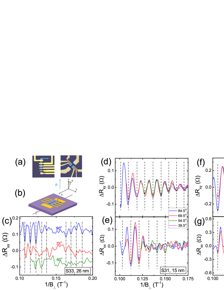
First, we show the WTe2 thin film below 26 nm is a 2D system, contrary to previous suggestions that it is a 3D bulk system Na et al. (2016); Wang et al. (2016c). Figure 1a shows optical images of two typical devices, S33 (green) and S54 (blue). Figure 1b shows a schematic diagram of the measurement configuration for angle-dependent magneto-transport measurement. The current is driven through the plane of the WTe2 crystal, and when the magnetic field is rotated from out-of-plane to in-plane, it is always perpendicular to the current. We observe quantum oscillations related to the Landau quantization both in and . Clear quantum oscillation signals and are obtained by subtracting a polynomial background from and as shown in Figs. 1c1g.
In bulk WTe2 the Fermi surface is three dimensional, so quantum oscillations are observed for any magnetic field orientation, and have been studied for all three field orientations with respect to the crystal axes Zhu et al. (2015); Rhodes et al. (2015). Only a small mass anisotropy is found for different transport directions Thoutam et al. (2015). In our thickest sample S33 (26 nm), we observe bulk behavior of the quantum oscillations when the sample is tilted in the applied magnetic field as shown in Fig. 1c. With the magnetic field perpendicular to the sample (, blue trace), there are clear oscillations in , periodic in which is the perpendicular component of magnetic field, . However, the period and amplitude of these oscillations vary with the tilt angle , indicating that the Fermi surface is three dimensional. In thinner samples, 15 nm or less, we find that both the period and amplitude of the quantum oscillations depend only on , as shown in Figs. 1d1g. This indicates that there is a crossover from a 3D to a 2D Fermi surface when the sample thickness is reduced from 26 nm (S33) to 15 nm (S31).
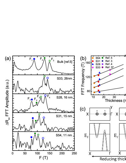
Next we show another aspect of the changing electronic structure as the WTe2 films are made thinner. Figure 2a shows a fast Fourier transform (FFT) spectrum of quantum oscillations in from several samples, ranging from bulk to 11 nm thick. The FFT of the bulk sample obtained from our previous work at 2.5 K shows three frequency peaks, 86.3 T, 130.2 T and 140.1 T Xiang et al. (2015a). The absence of a fourth peak around 162 T reported in Zhu et al. (2015); Cai et al. (2015); Rhodes et al. (2015) may be due to the relatively high measurement temperature and low mobility of carrier in that band. In order to resolve quantum oscillations from low mobility bands, all thin film samples were measured at millikelvin temperature and magnetic fields up to 10 T. We note that the quantum oscillation signals from the WTe2 thin films are relative weak, reducing the signal to noise ratio in the FFT spectrum and hindering observation of the first two frequency peaks in S33. But for most samples (S28, S31 and S54) four frequency peaks can be observed. Sample S28 has the highest signal to noise ratio, so four strong frequency peaks can be clearly observed, as indicated by the squares and circles in Fig. 2a, which is consistent with the four frequencies observed in bulk samples Zhu et al. (2015); Cai et al. (2015); Rhodes et al. (2015). However, the peaks of the thin film samples shift to lower frequency compared to those of bulk samples.
To better illustrate the shift of frequency as the thickness is reduced, we plot the FFT frequency vs thickness as shown in Fig. 2b. The frequencies of bulk samples are from Refs. Zhu et al. (2015); Cai et al. (2015); Xiang et al. (2015a); Rhodes et al. (2015) and their thicknesses are set as infinite compared with the thin film samples. The solid lines are guides to the eye showing how each frequency shifts as the sample thickness is reduced. The frequencies , , and correspond to the frequency peaks indicated by the solid circle, solid square, open square and open circle in the Fig. 2a, respectively. It can be seen that there is a trend that the FFT frequency becomes smaller as the sample thickness is reduced. And recent work on a three layer WTe2 sample shows even smaller quantum oscillation frequency Fatemi et al. (2017). The frequency of quantum oscillations is related to the extremal cross-sectional areas of the Fermi surface perpendicular to the magnetic field. The lower frequencies correspond to smaller area of Fermi pockets. One possibility is that the reduction in the size of the Fermi pockets is caused by a change in the Fermi level. However, since both the electron and hole pockets are simultaneously occupied in WTe2, changes in the Fermi level would cause the area of some Fermi pockets to increase while others decrease as the samples are made thinner. This is not the case here. The other possibility is change of band structure as illustrated in the Fig. 2c, which shows schematic diagrams of how a change of band structure could decrease the size of both electron and hole pockets. As the thickness of the samples is reduced (right to left), the conduction band minima and valence band maxima move apart, (bottom panel of Fig. 2c), which reduces the size of both electron and hole pockets as illustrated in the top panel. A similar confinement-induced band structure change has been observed in MoS2, where the indirect band gap is changed from a bulk value of 1.29 eV to over 1.90 eV Mak et al. (2010), and in MoTe2, a relative compound of WTe2, where few layer samples shows band gap opening Keum et al. (2015).This indicates it may be possible to observe band gap opening in even thinner WTe2 thin films, which is consistent with two recent works on the band gap opening in monolayer samples Zheng et al. (2016); Fei et al. (2016).
Because the carrier density is proportional to the size of the Fermi pocket, a decrease of the Fermi pocket size should also result in a decrease of carrier density. We calculate the 2D carrier density from quantum oscillation frequencies in our high signal to noise ratio sample S28 (16 nm) by , is cm-2 where and are spin and valley degeneracy, is electron charge, is Plank constant and is the sum of T, T, T and T. This corresponds to a 3D carrier density cm-3, very close to cm-3 from the 13 nm sample of Ref. Woods et al. (2016), and similar to cm-3 from the 15.6 nm sample of Ref. Na et al. (2016). Therefore, the change of Fermi pocket size explains the unexpected reduction of carrier density as the samples become thinner as reported in Refs. Na et al. (2016); Woods et al. (2016).
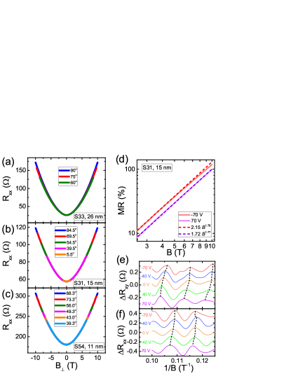
Now we discuss the impact of thickness-dependent electronic structure of WTe2 on its MR. In bulk samples, the angle-dependent as a function of magnetic field exhibits a 3D-like scaling law, with Thoutam et al. (2015). In contrast, here we find of the thin samples, S31 and S54, depends only on the perpendicular component of the magnetic field (see Figs. 3b and 3c) while the thick sample S33 does not: traces at different angles deviates from each other at high magnetic field (see Fig. 3a). This indicates that the thin samples are 2D, while the thick sample are not, which is consistent with the angle-dependent quantum oscillation results in Fig. 2.
The unsaturated MR in WTe2 is believed to be due to perfect electron and hole compensation, as described by the two-band model Ali et al. (2014); Pletikosić et al. (2014); Zhu et al. (2015); Cai et al. (2015); Xiang et al. (2015a); Zhao et al. (2015); Lv, H. Y. et al. (2015). If the electron and hole density are not equal, the MR will show a deviation at certain field, and the larger the difference between electron and hole density, the smaller field at which the deviation occurs Ali et al. (2014); Fatemi et al. (2017). The decrease of the carrier density as the sample thickness is reduced, as observed in Fig. 2, implies it is possible to use an electric field to tune the carrier density in a thin sample, which could provide a method to test the origin of the peculiar MR in WT2. In the sample S31 (15 nm), we measure the MR, defined as , at different back-gate voltages () from 70 V to -70 V. Figure 3d shows MR at 70 V and -70 V. While the MR at 70 V is well described by a simple power law up to 10 T, closed to the MR obtain from two-band model, the MR at -70 V starts to deviate from the power law at 5 T. For V this deviation occurs at 8 T (See Fig. S4(c) in Supplementary Materials Sup ). Because a positive (negative) decreases (increases) the hole density and increases (decreases) the electron density, it means that the electron and hole density are nearly equal at 70 V. When is changed from 70 V to -70 V, the Fermi level shifts down and the total electron density gradually become smaller than the total hole density. In addition, we observed that the back-gate also changes the quantum oscillations of S31 as shown in Figs. 3e and 3f. It can be seen that the maxima of quantum oscillations as indicated by the dashed lines in and gradually shift to lower magnetic field as the is changed from 70 V to -70 V. This indicates that the back-gate start to tune the carrier density, which consistent with the observation in Fig. 3d. With even thinner, the back-gate could be more effective to change the Fermi level, as observed in Refs. Fatemi et al. (2017); Zhang et al. (2017).
In summary, we observed thickness-dependent electronic structure in WTe2 thin films, by studying quantum oscillations from magneto-transport measurements. One finding is a crossover from a 3D to a 2D electronic system when the sample thickness is less than 26 nm, contrary to the assumptions in previous studies Wang et al. (2016c); Na et al. (2016). FFT analysis shows that the size of the Fermi pockets becomes smaller as the samples are made thinner, indicating the overlap between conduction band minima and valence band maxima becomes smaller. This explains why the carrier density decreases as the sample thickness is reduced Na et al. (2016); Woods et al. (2016), and implies it is promising to open a band gap in even thinner samples and realize the 2D topological insulator Qian et al. (2014). In addition, quadratic MR also shows a crossover from 3D to 2D behavior as the samples are made thinner, while gating is shown to affect both the quadratic MR and the quantum oscillations of a thin sample by tuning its carrier density.
Acknowledgements.
We thank Shouyi Xie, Sven Rogge, Haifeng Feng and Yi Du for technical assistance, and thank Menno Veldhorst for helpful discussions. We acknowledge support from the ARC Discovery Project Scheme (DP160100077 and DP130102956) and an ARC Professional Future Fellowship (FT130100778). This work was performed in part using facilities of the NSW and ACT Nodes of the Australian National Fabrication Facility.References
- Ali et al. (2014) M. N. Ali, J. Xiong, S. Flynn, J. Tao, Q. D. Gibson, L. M. Schoop, T. Liang, N. Haldolaarachchige, M. Hirschberger, N. P. Ong, and R. J. Cava, Nature 514, 205 (2014).
- Pletikosić et al. (2014) I. Pletikosić, M. N. Ali, A. V. Fedorov, R. J. Cava, and T. Valla, Phys. Rev. Lett. 113, 216601 (2014).
- Zhu et al. (2015) Z. Zhu, X. Lin, J. Liu, B. Fauqué, Q. Tao, C. Yang, Y. Shi, and K. Behnia, Phys. Rev. Lett. 114, 176601 (2015).
- Cai et al. (2015) P. L. Cai, J. Hu, L. P. He, J. Pan, X. C. Hong, Z. Zhang, J. Zhang, J. Wei, Z. Q. Mao, and S. Y. Li, Phys. Rev. Lett. 115, 057202 (2015).
- Xiang et al. (2015a) F.-X. Xiang, M. Veldhorst, S.-X. Dou, and X.-L. Wang, EPL (Europhysics Letters) 112, 37009 (2015a).
- Zhao et al. (2015) Y. Zhao, H. Liu, J. Yan, W. An, J. Liu, X. Zhang, H. Wang, Y. Liu, H. Jiang, Q. Li, Y. Wang, X.-Z. Li, D. Mandrus, X. C. Xie, M. Pan, and J. Wang, Phys. Rev. B 92, 041104 (2015).
- Lv, H. Y. et al. (2015) Lv, H. Y., Lu, W. J., Shao, D. F., Liu, Y., Tan, S. G., and Sun, Y. P., EPL 110, 37004 (2015).
- Das et al. (2016) P. K. Das, D. Di Sante, I. Vobornik, J. Fujii, T. Okuda, E. Bruyer, A. Gyenis, B. E. Feldman, J. Tao, R. Ciancio, G. Rossi, M. N. Ali, S. Picozzi, A. Yadzani, G. Panaccione, and R. J. Cava, Nature Communications 7, 10847 (2016).
- Jiang et al. (2015) J. Jiang, F. Tang, X. C. Pan, H. M. Liu, X. H. Niu, Y. X. Wang, D. F. Xu, H. F. Yang, B. P. Xie, F. Q. Song, P. Dudin, T. K. Kim, M. Hoesch, P. K. Das, I. Vobornik, X. G. Wan, and D. L. Feng, Phys. Rev. Lett. 115, 166601 (2015).
- Thoutam et al. (2015) L. R. Thoutam, Y. L. Wang, Z. L. Xiao, S. Das, A. Luican-Mayer, R. Divan, G. W. Crabtree, and W. K. Kwok, Physical Review Letters 115, 046602 (2015).
- Rhodes et al. (2015) D. Rhodes, S. Das, Q. R. Zhang, B. Zeng, N. R. Pradhan, N. Kikugawa, E. Manousakis, and L. Balicas, Physical Review B 92, 125152 (2015).
- Behnia (2015) K. Behnia, Physics , 71 (2015).
- Soluyanov et al. (2015) A. A. Soluyanov, D. Gresch, Z. Wang, Q. Wu, M. Troyer, X. Dai, and B. A. Bernevig, Nature 527, 495 (2015).
- Wu et al. (2016) Y. Wu, D. Mou, N. H. Jo, K. Sun, L. Huang, S. L. Bud’ko, P. C. Canfield, and A. Kaminski, Physical Review B 94, 121113 (2016).
- Wang et al. (2016a) C. Wang, Y. Zhang, J. Huang, S. Nie, G. Liu, A. Liang, Y. Zhang, B. Shen, J. Liu, C. Hu, Y. Ding, D. Liu, Y. Hu, S. He, L. Zhao, L. Yu, J. Hu, J. Wei, Z. Mao, Y. Shi, X. Jia, F. Zhang, S. Zhang, F. Yang, Z. Wang, Q. Peng, H. Weng, X. Dai, Z. Fang, Z. Xu, C. Chen, and X. J. Zhou, Physical Review B 94, 241119 (2016a).
- Feng et al. (2016) B. Feng, Y.-H. Chan, Y. Feng, R.-Y. Liu, M.-Y. Chou, K. Kuroda, K. Yaji, A. Harasawa, P. Moras, A. Barinov, W. Malaeb, C. Bareille, T. Kondo, S. Shin, F. Komori, T.-C. Chiang, Y. Shi, and I. Matsuda, Physical Review B 94, 195134 (2016).
- Sánchez-Barriga et al. (2016) J. Sánchez-Barriga, M. G. Vergniory, D. Evtushinsky, I. Aguilera, A. Varykhalov, S. Blügel, and O. Rader, Physical Review B 94, 161401 (2016).
- Bruno et al. (2016) F. Y. Bruno, A. Tamai, Q. S. Wu, I. Cucchi, C. Barreteau, A. de la Torre, S. McKeown Walker, S. Riccò, Z. Wang, T. K. Kim, M. Hoesch, M. Shi, N. C. Plumb, E. Giannini, A. A. Soluyanov, and F. Baumberger, Physical Review B 94, 121112 (2016).
- Wang et al. (2016b) Y. Wang, E. Liu, H. Liu, Y. Pan, L. Zhang, J. Zeng, Y. Fu, M. Wang, K. Xu, Z. Huang, Z. Wang, H.-Z. Lu, D. Xing, B. Wang, X. Wan, and F. Miao, Nature Communications 7, 13142 (2016b).
- Qian et al. (2014) X. Qian, J. Liu, L. Fu, and J. Li, Science 346, 1344 (2014).
- Kane and Mele (2005a) C. L. Kane and E. J. Mele, Physical Review Letters 95, 146802 (2005a).
- Kane and Mele (2005b) C. L. Kane and E. J. Mele, Physical Review Letters 95, 226801 (2005b).
- Bernevig and Zhang (2006) B. A. Bernevig and S.-C. Zhang, Physical Review Letters 96, 106802 (2006).
- Bernevig et al. (2006) B. A. Bernevig, T. L. Hughes, and S.-C. Zhang, Science 314, 1757 (2006).
- König et al. (2007) M. König, S. Wiedmann, C. Brüne, A. Roth, H. Buhmann, L. W. Molenkamp, X.-L. Qi, and S.-C. Zhang, Science 318, 766 (2007).
- Wang et al. (2015) L. Wang, I. Gutiérrez-Lezama, C. Barreteau, N. Ubrig, E. Giannini, and A. F. Morpurgo, Nature Communications 6, 8892 (2015).
- Wang et al. (2016c) L. Wang, I. Gutiérrez-Lezama, C. Barreteau, D.-K. Ki, E. Giannini, and A. F. Morpurgo, Physical Review Letters 117, 176601 (2016c).
- Na et al. (2016) J. Na, A. Hoyer, L. Schoop, D. Weber, B. V. Lotsch, M. Burghard, and K. Kern, Nanoscale 8, 18703 (2016).
- Woods et al. (2016) J. M. Woods, J. Shen, P. Kumaravadivel, Y. Pang, Y. Xie, G. A. Pan, M. Li, E. I. Altman, L. Lu, and J. J. Cha, arXiv:1606.05756 (2016).
- Liu et al. (2016) W. L. Liu, M. L. Chen, X. X. Li, S. Dubey, T. Xiong, Z. M. Dai, J. Yin, W. L. Guo, J. L. Ma, Y. N. Chen, J. Tan, D. Li, Z. H. Wang, W. Li, V. Bouchiat, D. M. Sun, Z. Han, and Z. D. Zhang, arXiv:1608.04801 (2016).
- Liu et al. (2017) X. Liu, Z. Zhang, C. Cai, S. Tian, S. Kushwaha, H. Lu, T. Taniguchi, K. Watanabe, R. J. Cava, S. Jia, and J.-H. Chen, arXiv:1702.05876 (2017).
- Lee et al. (2015) C.-H. Lee, E. C. Silva, L. Calderin, M. A. T. Nguyen, M. J. Hollander, B. Bersch, T. E. Mallouk, and J. A. Robinson, Scientific Reports 5, 10013 (2015).
- Ye et al. (2016) F. Ye, J. Lee, J. Hu, Z. Mao, J. Wei, and P. X.-L. Feng, Small 12, 5802 (2016).
- Naylor et al. (2017) C. H. Naylor, W. M. Parkin, Z. Gao, H. Kang, M. Noyan, R. B. Wexler, L. Z. Tan, Y. Kim, C. E. Kehayias, F. Streller, Y. R. Zhou, R. Carpick, Z. Luo, Y. W. Park, A. M. Rappe, M. Drndić, J. M. Kikkawa, and A. T. C. Johnson, 2D Materials 4, 021008 (2017).
- Zheng et al. (2016) F. Zheng, C. Cai, S. Ge, X. Zhang, X. Liu, H. Lu, Y. Zhang, J. Qiu, T. Taniguchi, K. Watanabe, S. Jia, J. Qi, J.-H. Chen, D. Sun, and J. Feng, Advanced Materials 28, 4845 (2016).
- Fei et al. (2016) Z. Fei, T. Palomaki, S. Wu, W. Zhao, X. Cai, B. Sun, P. Nguyen, J. Finney, X. Xu, and D. H. Cobden, arXiv:1610.07924 (2016).
- Shoenberg (1984) D. Shoenberg, Magnetic oscillations in metals (Cambridge University Press, Cambridge, 1984).
- Qu et al. (2010) D.-X. Qu, Y. S. Hor, J. Xiong, R. J. Cava, and N. P. Ong, Science 329, 821 (2010).
- Analytis et al. (2010) J. G. Analytis, R. D. McDonald, S. C. Riggs, J.-H. Chu, G. S. Boebinger, and I. R. Fisher, Nat Phys 6, 960 (2010).
- Xiang et al. (2015b) F.-X. Xiang, X.-L. Wang, M. Veldhorst, S.-X. Dou, and M. S. Fuhrer, Phys. Rev. B 92, 035123 (2015b).
- Yeoh et al. (2010) L. A. Yeoh, A. Srinivasan, T. P. Martin, O. Klochan, A. P. Micolich, and A. R. Hamilton, Review of Scientific Instruments 81, 113905 (2010).
- Fatemi et al. (2017) V. Fatemi, Q. D. Gibson, K. Watanabe, T. Taniguchi, R. J. Cava, and P. Jarillo-Herrero, Phys. Rev. B 95, 041410 (2017).
- Mak et al. (2010) K. F. Mak, C. Lee, J. Hone, J. Shan, and T. F. Heinz, Phys. Rev. Lett. 105, 136805 (2010).
- Keum et al. (2015) D. H. Keum, S. Cho, J. H. Kim, D.-H. Choe, H.-J. Sung, M. Kan, H. Kang, J.-Y. Hwang, S. W. Kim, H. Yang, K. J. Chang, and Y. H. Lee, Nat Phys 11, 482 (2015).
- (45) See Supplemental Material at [URL will be inserted by publisher] for [Raw data of quantum oscillations before low pass filtering, power law fitting of MR for different samples, and MR of S31 in linear scale at different back-gate voltages.] .
- Zhang et al. (2017) E. Zhang, R. Chen, C. Huang, J. Yu, K. Zhang, W. Wang, S. Liu, J. Ling, X. Wan, H.-Z. Lu, and F. Xiu, Nano Letters 17, 878 (2017).