Tunneling conductance in semiconductor-superconductor hybrid structures
Abstract
We study the differential conductance for charge tunneling into a semiconductor wire–superconductor hybrid structure, which is actively investigated as a possible scheme for realizing topological superconductivity and Majorana zero modes. The calculations are done based on a tight-binding model of the heterostructure using both a Blonder-Tinkham-Klapwijk approach and a Keldysh non-equilibrium Green’s function method. The dependence of various tunneling conductance features on the coupling strength between the semiconductor and the superconductor, the tunnel barrier height, and temperature is systematically investigated. We find that treating the parent superconductor as an active component of the system, rather than a passive source of Cooper pairs, has qualitative consequences regarding the low-energy behavior of the differential conductance. In particular, the presence of sub-gap states in the parent superconductor, due to disorder and finite magnetic fields, leads to characteristic particle-hole asymmetric features and to the breakdown of the quantization of the zero-bias peak associated with the presence of Majorana zero modes localized at the ends of the wire. The implications of these findings for the effort toward the realization of Majorana bound states with true non-Abelian properties are discussed.
I Introduction
The search for quantum states of matter characterized by nontrivial topological properties has gained significant momentum in recent years motivated, in part, by the discovery of topological insulators Hasan and Kane (2010); Qi and Zhang (2011); Bernevig (2013) and by the exciting prospect of using topological objects, such as the Majorana zero modes, Alicea (2012); Leijnse and Flensberg (2012); Beenakker (2013); Stanescu and Tewari (2013) as a platform for fault tolerant quantum computation. Nayak et al. (2008); Stanescu (2017) The proposal for engineering topological superconductors capable of supporting Majorana zero modes that has generated the most promising experimental results involves a semiconductor nanowire with strong spin-orbit coupling proximity-coupled to a standard s-wave superconductor in the presence of an applied magnetic field.Lutchyn et al. (2010); Oreg et al. (2010) Upon increasing the magnetic field, the system undergoes a topological quantum phase transitionRead and Green (2000); Sau et al. (2010) from a topologically-trivial superconductor to a topological superconductor with mid-gap Majorana zero modes localized near the ends of the wire. The presence of the Majorana bound states can be probed by tunneling charge into the end of the wire, which is predicted to generate a zero-bias conductance peak that is quantized () at zero temperature.Sengupta et al. (2001); Law et al. (2009); Flensberg (2010); Wimmer et al. (2011); Fidkowski et al. (2012) These theoretical proposals and predictions have led to an impressive experimental effortMourik et al. (2012); Deng et al. (2012); Das et al. (2012); Finck et al. (2013); Chang et al. (2015); Albrecht et al. (2016); Zhang et al. (2016); Deng et al. (2016); Chen et al. (2016) for realizing Majorana zero modes in semiconductor-superconductor hybrid structures. The results of this effort are promising, but a conclusive demonstration of the realization of Majorana bound states in the laboratory remains elusive.
A serious problem is the persistence of significant discrepancies between theory and experiment. While the theoretical possibility of realizing topological superconductivity and Majorana zero modes in semiconductor-superconductor structures that satisfy certain requirements is beyond any reasonable doubt, understanding how well real devices realized in the laboratory satisfy these requirements remains a serious challenge. In addition to careful systematic measurements, overcoming this challenge calls for theoretical studies that go beyond idealized conditions and incorporate all relevant details associated with real devices. Since charge tunneling is, so far, the preferred method of detecting the presence of Majorana zero modes, significant theoretical effort was devoted to numerical and analytical studies of the tunneling differential conductance using both normal metalStanescu et al. (2011); Pientka et al. (2012); Prada et al. (2012); Lin et al. (2012); Rainis et al. (2013); Stanescu et al. (2014); Yan and Wan (2014); Setiawan et al. (2015); Liu et al. (2017) and superconductorPeng et al. (2015); Sharma and Tewari (2016); Chevallier and Klinovaja (2016); Setiawan et al. (2017) leads. Most of these studies, however, do not consider explicitly the parent s-wave superconductor; instead, its role is reduced to that of a passive source of Cooper pairs for the semiconductor nanowire. Recently, it has been emphasized that the parent superconductor should be treated as an active ingredient in the physics of the heterostructure.Reeg and Maslov (2017); Stanescu and Sarma (2017) This treatment of the semiconductor wire and the parent superconductor on equal footing leads to a renormalization of the low-energy modes in the hybrid systemStanescu and Sarma (2017) and the emergence of additional conductance peaks at energies corresponding to the bulk gap of the parent superconductor.Reeg and Maslov (2017)
In this work we investigate theoretically the tunneling conductance of a normal-metal – semiconductor-wire – superconductor hybrid structure and demonstrate that the explicit treatment of the parent superconductor as an active component of the system has major consequences not only at energies on the order of the bulk superconducting gap, but all the way down to zero energy. Our findings are based on a systematic numerical analysis of a tight-binding model of the heterostructure. The conductance calculations are carried out within both the Blonder-Tinkham-Klapwijk (BTK) theoryBlonder et al. (1982) and the Keldysh non-equilibrium Green’s function formalismRammer and Smith (1986). To gain a better physical understanding of the low-energy features revealed by the differential conductance, we compare these features with the local density of states. We establish the qualitative features that characterize the dependence of tunneling conductance on the coupling strength between the semiconductor wire and the parent superconductor, the strength of the tunnel barrier, and temperature. We also consider the possibility of sub-gap states being present in the parent superconductor and identify the consequences of these states hybridizing with low-energy states in the wire. We find that the presence of sub-gap states leads to characteristic particle-hole asymmetric features in the low-energy differential conductance and to a breakdown of the zero-bias peak quantization at zero temperature. Our findings suggest that a detailed modeling of the parent superconductor, including the possible presence of disorder-induced sub-gap states in the presence of a finite magnetic field, is a strong requirement for any attempt to quantitatively (and, at this stage, even qualitatively) reproduce the experimentally measured differential conductance.
The remainder of this paper is organized as follows. In Sec. II we introduce a tight-binding model for the normal-metal – semiconductor-wire – superconductor hybrid structure (Sec. II.1) and briefly describe the BTK-type formalism (Sec. II.2) and the Keldysh approach (Sec. II.3) for calculating the differential conductance. The results of our numerical analysis are presented in Sec. III. First, we compare the two approaches for calculating the tunneling conductance and establish the correspondence between the differential conductance (in the low tunneling regime) and the local density of states (Sec. III.1). The dependence of the low-energy features on the transparency of the semiconductor-superconductor interface and the tunnel barrier height is discussed in Sec. III.2. We show that additional features associated with charge transport via quasiparticles in the parent superconductor occur at energies larger than the bulk superconducting gap. The effects of disorder-induced sub-gap states in the parent superconductor are investigated in Sec.III.3 and the dependence of the Majorana-induced zero-bias conductance peak on the relevant parameters (i.e., tunnel barrier height, temperature, and sub-gap states density) is summarized in Sec. III.4. Our conclusions are presented in Sec. IV.
II Theoretical model
In this section we introduce the tight-binding model for the normal-metal – semiconductor-wire – superconductor hybrid structure and briefly describe the BTK and Keldysh methods for calculating the differential conductance. Both approaches explicitly incorporate the parent superconductor.
II.1 Tight-binding Hamiltonian
We consider charge tunneling from a normal metal lead into a semiconductor wire - superconductor hybrid structure through a controllable potential barrier. The Hamiltonian describing the system has the following generic form:
| (1) |
where , , and describe the normal metal, semiconductor wire, and superconductor components, respectively, the next two terms describe the coupling between the semiconductor wire and the metallic lead () and the coupling between the wire and the parent superconductor (), while includes contributions from external fields, such as magnetic fields and electrostatic potentials. The specific form of each term in Eq. (1) depends on on the degree of complexity that we want to incorporate into the model. In this study we consider a simple tight-binding description of the hybrid system involving a lattice consisting of coupled parallel chains. Specifically, we have
| (2) |
where labels the position, with designating the chain and the position along the chain, or is a nearest neighbor vector, is the hopping matrix element, and the chemical potential of the metallic lead. Using spinor notation, the electron creation operator on site is . The semiconductor wire (including the applied external fields) is described by the tight-binding Hamiltonian
| (3) | |||||
where is the electron creation operator on the site of the semiconductor wire, with and , is the nearest-neighbor hopping, or is a nearest neighbor vector, while and are (positive) unit vectors in the x- and y-direction, respectively, is the chemical potential, and are the Rashba spin-orbit coupling coefficients. The position-dependent potential describes the tunneling barrier and additional back-gate-induced potentials, while represents the Zeeman splitting. The matrices , with , represent Pauli matrices associated with the spin degree of freedom. The parent superconductor is described within the Bogoliubov-de Gennes (BdG) formalism by
| (4) | |||||
where is the electron creation operator on the site of the superconducting chains, with and , is the nearest-neighbor hopping matrix element, the chemical potential of the superconductor, and is the superconducting gap. We assume that the superconductor is equal to or longer than the semiconductor wire, . The coupling between the semiconductor wire and the metallic lead is described by the term
| (5) |
where the nearest-neighbor hopping quantifies the coupling strength, while and label the sites at the right end of the metallic lead and the left end of the semiconductor wire, respectively. Finally, the coupling between the semiconductor and the superconductor is described by the term
| (6) |
where , is the hopping across the semiconductor-superconductor (SM-SC) interface, while and designate annihilation operators on the SM and SC sides, respectively.
It may be convenient to use a Green’s function formalism and calculate the effective Green function for the semiconductor wire by integrating out the degrees of freedom of the parent superconductor.Stanescu and Tewari (2013) The proximity effect induced by the superconductor is captured by a self-energy term,
| (7) |
where is the Green function of the parent superconductor at the SM-SC interface. Assuming that the parent superconductor is a truly bulk system (i.e., wide enough and thick enough), the self-energy becomes local,Stanescu and Tewari (2013) , with
| (8) |
where is the surface density of states of the bulk superconductor at the chemical potential and is a proximity-induced shift of the SM chemical potential. The matrices , with , represent Pauli matrices associated with the particle-hole degree of freedom. We define the effective SM-SC coupling as
| (9) |
Note that here we do not discuss the physics associated with the finite wire thickness in the direction perpendicular to the SM-SC interface (i.e., the -direction). This is critical when considering electrostatic effects, such as those generated by back-gate potentials. In general, the effective SM-SC coupling is a band-dependent quantity proportional to the amplitude squared of the wave-functions (corresponding to a given confinement-induced band) at the SM-SC interface and may involve band off-diagonal contributions.Stanescu and Tewari (2013) In the weak-coupling limit, , the self-energy (8) can be approximated at low energy by the anomalous contribution
| (10) |
Note that in this approximation the proximity-induced gap (defined as the minimum quasiparticle gap in the absence of an applied magnetic field) is and the minimum critical Zeeman field associated with the topological quantum phase transition is . However, in general the critical field and the induced gap have different values.Sticlet et al. (2016); Stanescu and Sarma (2017) To describe the low-energy spectral properties of the hybrid structure it is convenient to use the density of states (DOS) and the local density of states (LDOS) at the end of the wire. In terms of the effective wire Green’s function we have
| (11) | |||||
| (12) |
II.2 BTK Formalism
The calculation of the differential conductance using the Blonder-Tinkham-Klawijk (BTK) formalismBlonder et al. (1982) involves calculating the reflection and transmission coefficients for incoming (and outgoing) plane waves by solving the Bogoliubov-de Gennes (BdG) equation for the total Hamiltonian given by Eq. (1) with appropriate boundary conditions. The Schrödinger equation that determines the reflection and transmission coefficients is
where is the first quantized BdG Hamiltonian corresponding to Eq. (1) and . For convenience, we define the transverse modes , with , characterized by the wave functions . Each transport channel is labeled by the pair of quantum numbers corresponding to a given transverse mode and spin orientation and the reflection and transmission coefficients are matrices with matrix elements indexed by these channel labels.
Consider now an incoming plane wave in channel . To ensure that the wave function entering the normal lead is a (propagating) plane wave, we impose (propagating) boundary conditions involving the first two sites of each chain, i.e., and . Note that similar propagating boundary conditions involving two sites at the rightmost end of the superconductor, i.e., and , correspond to an outgoing plane wave. Specifically, the (incoming) boundary conditions at the left end of the metallic lead are
| (22) | |||||
| (27) | |||||
| (32) |
where and are the normal and anomalous reflection coefficients, respectively, is the lattice constant, while and are wave vectors in the normal lead at energies and , respectively,
| (33) |
with . Similarly, the outgoing plane wave dictates the boundary conditions at the rightmost end of the bulk superconductor chains,
| (38) | |||||
| (43) |
where and are the normal and anomalous transmission coefficients, respectively, while and are wave vectors in the bulk superconductor
| (44) |
with and . To solve the BdG equation (II.2) with the boundary conditions (27) and (38) it is convenient to express the wave function components corresponding to in terms of the reflection and transmission coefficients corresponding to the incoming channel . Thus, Eq. (II.2) reduces to a system of linear equations with unknown coefficients that include the wave function components , with , and the reflection and transmission coefficients. Writing theses unknown coefficients as a vector with components, we have
| (45) |
Explicitly, we define the components of the new vector to be the same as the wave function components, , for , while
| (46) | |||||
where and are BCS coherence factors:
| (47) |
The matrix introduces frequency-dependent correction at the boundaries,
| (48) | |||
with
| (49) | |||
All other elements of are zero, if or . Finally, the vector contains the “free terms” from the boundary conditions (i.e., those that do not depend on the reflection and transmission coefficients), which are associated with the incoming plane wave. Explicitly, we have
| (50) |
and for . Note that all the information about the boundary conditions is contained in the matrix and the vector . The coefficients and are obtained by solving Eq. (45) times, once for each incoming channel.
An interesting observation is that the matrix in Eq. (45) has the structure of a Green’s function, . Generalizing the approach used in Sec. II.1 to calculate the effective Green’s function for the semiconductor wire, we integrate out the degrees of freedom of the bulk superconductor and write an equation for the reflection coefficients involving only states in the semiconductor and the metallic lead:
| (51) |
where , , and are the matrices corresponding to the first quantized Hamiltonians for the metallic lead, the semiconductor wire, and the lead-wire coupling, respectively, is the matrix corresponding to the boundary condition at the left end of the normal lead and is a “self-energy” contribution that incorporates the effect of the parent superconductor, including the the outgoing boundary conditions. Note that below the bulk gap there is no normal current (i.e., current carried by quasiparticles) in the superconductor; hence the outgoing boundary conditions become trivial and we have . In general, since the boundary conditions are diagonal in real space while is diagonal in mode space, the self energy has to be calculated numerically. Nonetheless, using Eq. (51) instead of Eq. (45) provides significant advantages, as one can calculate the self-energy once, then solve the reduced equation repeatedly for different values of relevant parameters, such as potential barrier height and Zeeman field, instead of solving the full equation (45) for each set of parameters.
The differential conductance for tunneling into the hybrid structure can be written in terms of reflection coefficients asBlonder et al. (1982)
| (52) |
where is the bias voltage. To include the effect of finite temperature, the conductance is broadened by convolving it with the Fermi function. Explicitly, we have
| (53) |
where is the zero temperature conductance given by Eq. (52) at voltage bias .
II.3 Keldysh Formalism
Consider a normal metal-semiconductor junction. The current through the junction can be expressed in terms of the number operator for the component to the right of the junction as
| (54) |
where is the equilibrium quantum state of the composite system, is the total Hamiltonian, and is the number operator for the right component. The label indicates both position (on the right side of the junction) and spin. The number operator can only change if some electrons cross the junction. Hence, one can rewrite the current asBerthod and Giamarchi (2011)
| (55) |
where is the coupling between the metal and the semiconductor given by Eq. (6). The differential conductance can be extracted by taking the derivative of the current with respect to the bias voltage in the lead, . Notice that the propagator is the so-called lesser Green’s function at time .Rammer and Smith (1986) Using the relation between and the Keldysh Green’s function, Eq. (55) becomes
| (56) |
where we have used the property . Expanding in terms of Green’s functions for the left and right sub-systems, we have
| (57) | |||||
The Keldysh Green’s function becomes
where and are the retarded and advanced Green’s functions, respectively. Next, we take the derivative with respect to the bias voltage. We assume the voltage drops at the junction, so we only take the derivative in the Green’s function of the lead, (i.e., we assume that is independent of ). The main contribution comes from the derivative of the Fermi function with respect to the voltage, hence from , where . Explicitly, the differential conductance is given by
Finite temperature can be included in the same way as in the BTK method.
III Results
In this section we discuss the results of our numerical analysis focusing on features in the calculated differential conductance that are only present if the parent superconductor is explicitly treated as an active component of the system and on the dependence of the Majorana zero bias conductance peak on the relevant system parameters.
The numerical results described below are obtained by setting the chemical potentials for the metal and the superconductor ( and , respectively) to the middle of their respective bands. The other model parameters are chosen as follows: The lattice constant is nm along the wire (i.e., in the direction) and nm across the wire (i.e., in the direction); if the wire is m long, there are 100 sites in each SM chain. The hopping parameters are meV, meV, meV, meV, meV, meV, and meV. The spin orbit coupling parameters are meV and meV. The bias potential is applied to the metallic lead, which is sites long (the shortest length that is consistent with plane wave boundary conditions), while the superconductor is grounded.
We model the parent superconductor as a long, thick slab having sites in the direction (i.e., m) and sites in the direction. To handle the problem concerning the large number of degrees of freedom associated with the parent superconductor, we calculate the (surface) Green’s function of a large slab once and store the information. Subsequently, we “attach” this large superconductor to semiconductor wires (of various lengths) and calculate the corresponding interface self-energy, which completely contains the effect of the superconductor. More specifically, we first calculate numerically the superconductor Green’s function, which determines both the self energy given by (7) and the boundary-condition-dependent “self-energy” from Eq. (51), in the transverse mode space, where the problem is diagonal and can be solved separately for each of the modes. Then, we calculate the surface Green’s function for frequencies up to meV taking equally spaced values in the range to meV. If necessary, we extrapolate for frequencies in-between these these discrete values. Note that below the bulk gap (i.e., below meV), we can use the analytical solution given by Eq. (8). These calculated values of the surface Green’s function are stored for later use in the calculation of the self-energies corresponding to wires of different lengths.
III.1 Method comparison and differential conductance vs. LDOS
The BTKBlonder et al. (1982) and KeldyshRammer and Smith (1986) formalisms are two possible methods for calculating the differential conductance. Since the two approaches are formally rather different, the first question that we want to address is whether or not the predictions based on these methods are the same. In addition, when interpreting charge transport measurements on semiconductor -superconductor (SM-SC) Majorana hybrid structures it is essential to understand the connection between the measured differential conductance and the low-energy spectral properties of the hybrid system. To address these questions, we calculate the density of states (DOS) and the local density of states (LDOS) at the end of the wire for a nanowire of length m proximity-coupled to a meV superconductor so that the induced gap is meV. We compare these quantities with the differential conductance for tunneling into the end of the same wire, which is calculated using both methods described in the previous section. The results are shown in Fig. 1.
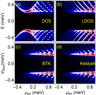
Panels (a) and (b) show the DOS and LDOS, respectively, as functions of the chemical potential and energy. The bottom panels in Fig. 1, i.e., (c) and (d), show the differential conductance calculated using the BTK and Keldysh methods. The “stripy” features are due to the quantization of states in a finite wire and reflect the variation of the eigenvalues of the BdG Hamiltonian with the chemical potential. In our model the energy difference between successive states becomes larger as the chemical potential increases. Note that corresponds to the bottom of the band, which is clearly revealed by the large DOS in panel (a). By contrast, there is no clear signature associated with the bottom of the band in the LDOS [panel (b)] or in the differential conductance [panels (c) and (d)]. This is due to the fact that the LDOS is calculated at the end of the proximitized wire adjacent to the potential barrier, where states from the bottom of the band have very low amplitude. These states are weakly coupled to the lead and, consequently, do not contribute significantly to the differential conductance, as shown in panels (c) and (d). Another way of understanding this behavior is in terms of velocity. Penetration of the barrier is determined by the group velocity. An electron occupying a state with higher velocity has a greater chance to get through the barrier and couple to the lead. Since the velocity vanishes at the bottom of the band, the corresponding states will have a small contribution to the conductance. As the chemical potential increases, the wavelength of the states is shortened and their velocity becomes larger, which results in higher values of the conductance.
Based on this analysis we conclude that (i) the BTK and Keldysh formalisms predict similar values for the differential conductance and (ii) the dependence of the differential conductance on the chemical potential and bias voltage is qualitatively similar to that of the LDOS at the end of the wire adjacent to the tunnel barrier. Of course, the second property holds in the weak tunneling regime,Berthod and Giamarchi (2011) but breaks down when the transparency of the barrier is large. In Fig. 1 the only notable difference between the differential conductance and the LDOS is the decrease of with increasing bias voltage , which is not reflected in the dependence of the LDOS on energy. To understand this behavior, we note that for voltage values below the gap of the parent superconductor charge can only travel through the superconductor as a supercurrent. Tunneling electrons into the wire involves anomalous (Andreev) reflection processesBlonder et al. (1982); He et al. (2014) (an incoming electron returns as a hole) and the probability for such a process depends on the properties of the quasiparticle states of the wire-superconductor hybrid system. Near the induced gap ( meV in Fig. 1), where every state is an almost equal blend of particles and holes, the probability of anomalous reflection is large, but it decreases at higher (in absolute value) energies, where the quasiparticles have a dominant particle or hole character.
We have verified our conclusions for a broad range of parameters, including bias voltage values larger than the parent superconductor gap, and we found them to be rather generic properties. Below we calculate the conductance using the most convenient method for a specific setup or physical aspect that we want to investigate. Since we are mostly interested in the weak tunneling regime, we will interpret the results as (approximately) representing the local density of states near the end of the wire-superconductor system adjacent to the tunnel barrier.
III.2 Dependence on the semiconductor-superconductor coupling strength and tunnel barrier height
Proximity coupling a semiconductor wire to a conventional superconductor results in the opening of an induced gap in the quasiparticle spectrum at the chemical potential. At zero momentum, , and in the absence of a magnetic field the induced gap is determined by the gap of the parent superconductor and by the effective semiconductor-superconductor (SM-SC) coupling constant . The simplest way to account for the emergence of an induced gap is to introduce a pairing potential in the effective BdG Hamiltonian for the wire. However, this approach fails to describe accurately the low-energy physics of the hybrid structure (i.e., the induced ”bulk” quasiparticle gaps and the in-gap bound states), with the exception of the weak coupling limit . However, experimentally-relevant devices are not in this limit and the explicit treatment of the parent superconductor, e.g., using Eq. (8), is necessary.Stanescu and Sarma (2017) What features of the differential conductance are directly related to the parent superconductor being an active component of the hybrid structure?
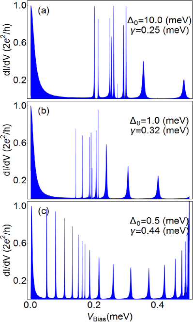
First, we consider the dependence of the low-energy features of a finite wire in the topological regime on the effective SM-SC coupling strength. The differential conductance as function the bias voltage for three different ratios is shown in Fig. 2. The calculations are done for a wire of length m in the presence of a Zeeman field meV. Note that the induced gap (i.e., the quasiparticle gap at ) is the same in all three cases, meV. However, the critical Zeeman splitting corresponding to the topological quantum phase transition (TQPT) is different, as it is determined by the effective coupling strength , rather than the induced gap.Stanescu and Sarma (2017); Sticlet et al. (2016) For the Zeeman field value used in the calculations, meV, all three systems are in the topological regime, as signaled by the presence of a Majorana-induced zero-bias conductance peak. The differential conductance in Fig. 2(a), which corresponds to , is the same as that predicted by the effective pairing approximation defined by Eq. 10. However, increasing the effective coupling [panels (b) and (c)] results in several effects that cannot be captured by this approximation. First, the weight of the Majorana-induced zero-bias peak (ZBP) decreases with increasing coupling. The main reason for this behavior is the fact that the spectral weight of the Majorana mode within the wire decreases with increasing coupling. In other words, as increases, the amplitude of the Majorana wave function within the wire (i.e., in the vicinity of the tunnel barrier) is reduced, while its amplitude within the parent superconductor (i.e., farther away from the tunnel barrier) is enhanced.Stanescu and Sarma (2017) This results in a lower “visibility” of the Majorana mode, as revealed by the ZBP. The second effect is the renormalization of the quasiparticle energies and the reduction of the topological gap.Stanescu and Sarma (2017) In essence, these effects are due to the fact that all low-energy states reside both in the wire and in the parent superconductor, with more and more spectral weight being transfered to the superconductor as the coupling strength increases.
The bias voltage range shown in Fig. 2 corresponds to energies below the gap of the parent superconductor. In this regime there is no normal current flowing through the superconductor. In the BTK approach, this means that it is sufficient to impose boundary conditions at the end of the normal lead. However, if we want to explore an energy window larger than the bulk gap, we have to supplement this with boundary conditions at the end of the parent superconductor. These boundary conditions account for the normal current carried by the quasiparticles in the parent superconductor. Note that these boundary conditions are diagonal in real space, while the superconductor Hamiltonian is diagonal in the mode space. Consequently, finding an analytical expression is rather difficult; instead, we calculate the self-energy (which incorporates the boundary conditions) numerically.
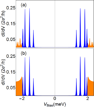
Including the normal transmission is required at bias voltages above the bulk gap, as demonstrated by the data shown in Fig. 3. Here we calculate the differential conductance for a short nanowire of length m coupled to a superconductor with meV. The effective semiconductor-superconductor coupling is meV. In the top panel, the differential conductance is calculated without including the contribution from the normal transmission through the parent SC. All the features in this panel represent anomalous current contributions, which become rather small at energies larger than the bulk gap. Note that there is no feature associated with the bulk gap edge. By contrast, in the bottom panel, which shows the full calculation that includes the normal current contribution, one can clearly observe an additional feature associated with the parent superconductor gap (orange/light gray area). The emergence of an additional conductance peak at the energy corresponding to the gap of the parent superconductor, which was recently discussed in Ref. Reeg and Maslov, 2017, confirms the the predictions of Ref. Cole et al., 2015, which are based on a local density of states analysis. The presence of features associated with the parent superconductor may generate certain difficulties when interpreting measurements for hybrid systems in the intermediate and strong coupling regimes. In these cases, the induced gap and the bulk gap of the parent superconductor have comparable values and, therefore, it is important to be able to distinguish the corresponding features. To this end, we analyze their dependence on the effective SM-SC coupling strength and on the tunnel barrier height.
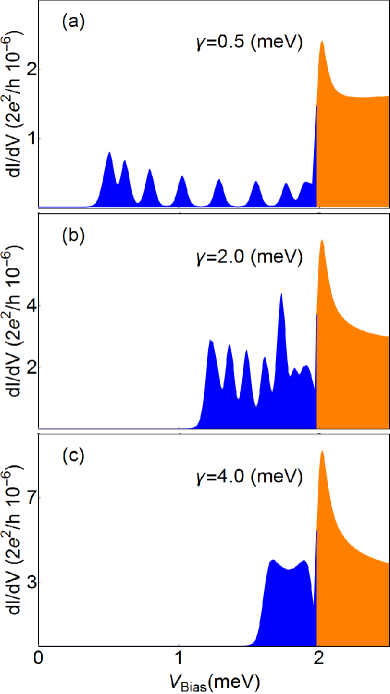
As discussed in the relation to Fig. 2, increasing the coupling between the semiconductor wire and the superconductor results in a renormalization of the low-energy spectrum and a reduction of the spectral weight within the wire. In addition, varying has a strong impact on the induced gap . In a multi-band system the specific dependence of the induced gap on the SM-SC coupling strength is rather complicated (except in the weak coupling regime) and involves additional parameters, such as the inter-band spacing and chemical potential.Stanescu and Sarma (2017) On the other hand, the feature in the differential conductance associated with the bulk superconductor has a relatively weak dependence on the SM-SC coupling, as shown in Fig. 4. In this figure, we calculate again at the differential conductance for a nanowire coupled to a superconductor with meV, but the length of the nanowire is now m; the effective SM-SC coupling takes three different values, and meV. Note, that the peak associated with the bulk gap edge becomes stronger with increasing . The features corresponding to low-energy semiconductor states (blue/darker gray) reveal the dependence of the induced gap on the SM-SC coupling and the proximity-induced energy renormalization discussed above. In particular, the energy spacing between successive low-energy states decreases with , so that a finite system characterized by discrete spectral features in the low-coupling regime [panel (a)] appears as having a continuous spectrum for a high-enough coupling strength [panel (c)].
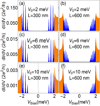
The dependence of the differential conductance on the tunnel barrier height is illustrated by the data shown in Fig. 5. We calculate as a function of the bias voltage for different barrier heights and two different wire lengths m and m. As before, the parent SC gap is meV, while the SM-SC coupling is meV. First, we note that the sub-gap features associated with the presence of the proximitized semiconductor wire (blue/darker gray) are strongly dependent on the length of the structure. By contrast, the parent superconductor contribution (orange/light gray) is practically independent on . In very short wires [panels (a), (c), and (e)] finite size quantization results in a discrete spectrum that generates a set of well-separated peaks in the differential conductance. Increasing the length of the wire [panels (b), (d), and (f)] reduces the intervals between successive peaks and, eventually, the spectrum becomes continuous [see, for example, Fig. 4 (c) and Fig. 6]. Note that the energy separation required for resolving discrete peaks depends on temperature, barrier transparency, and strength of the disorder present in the system. Above the bulk gap of the parent superconductor the semiconductor states hybridize with the superconductor states, which are overwhelmingly more numerous and, practically, determine the conductance response. Consequently, above the conductance is nearly independent of the wire length. Note, however, that the semiconductor plays an important role here. One can view all the hybrid states above the gap as superconductor states that have acquired a small “tail” that extends into the wire, including the region adjacent to the tunnel barrier. While the spectral weight carried by the tails is negligible, they are essential for ensuring the coupling between the normal lead and the “superconductor states.” In other words, the orange/light gray component of the differential conductance corresponds to hybrid states that have most of their spectral weight inside the parent superconductor, but have small tails extending into the barrier region.
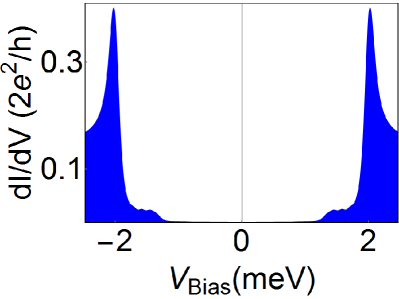
Varying the strength of the barrier potential affects the differential conductance both below and above the bulk gap (see Fig. 5). However, the differential conductance below the bulk gap (blue/darker gray) decreases faster than the conductance above the gap (orange/light gray) with increasing barrier potential. In fact, it is possible that for a large enough barrier potential the sub-gap conductance is “completely” suppressed (for a certain finite resolution), while the parent superconductor contribution is still measurable. A rigorous proof of this statement would imply performing a (self-consistent) calculation of the barrier potential profile, i.e., finding a (self-consistent) solution of the Schrödinger-Poisson equation. Intuitively, one can understand the effect of the barrier potential as resulting from the huge difference between the carrier densities in the semiconductor and the superconductor. Increasing the potential of the tunneling gate results in the potential barrier penetrating into the proximitized segment of the nanowire (i.e., under the superconductor) and “pushing away” the low-energy states that reside inside this component of the hybrid structure. On the other hand, the effect on the superconductor is negligible due to the screening provided by the large carrier density. To illustrate this effect, we calculate the differential conductance for a nanowire with m, similar to that corresponding to the right panels in Fig. 5, and a barrier potential profile that penetrates more into the wire. The results are shown in Fig. 6. Note the large difference between the conductance above the (bulk SC) gap and the sub-gap conductance, which appears as a small tail of the coherence peak. Remarkably, this shape looks quite similar to recent experimental results on epitaxial Al-InAs superconductor-semiconductor nanowiresChang et al. (2015) (more specifically, Fig. 5(c) for the half-shell device). To experimentally disentangle the induced and bulk contributions in the strong SM-SC coupling limit (where they have similar energy scales) we propose an analysis of the dependence of various features on the barrier potential. Starting, for example, with an extremely high barrier will only reveal bulk-type contributions.The induced features will progressively emerge as the potential barrier is lowered.
III.3 Parent superconductor with sub-gap states
So far we have assumed an “ideal” parent superconductor characterized by a perfectly clean gap, even in the presence of finite magnetic fields. However, real superconductors may have sub-gap states induced by disorder and finite external fields. Nonetheless, if a “dirty” superconductor has a few localized sub-gap states, we expect the system to behave qualitatively similar to a clean system. Indeed, the additional sub-gap states may hybridize with low-energy states from the semiconductor wire, which will result in the hybrid structure having additional low-energy modes and smaller quasiparticle gaps. However, the structure of the low-energy spectrum will be qualitatively similar to that of a clean system. Moreover, if the sub-gap states are localized far from the ends of the wire the Majorana modes will not be affected. The situation is completely different if the parent superconductor has a small but finite density of sub-gap states. In this situation, the entire gap is populated with hybrid states having most of their spectral weight inside the parent superconductor and some of it inside the semiconductor nanowire.Stanescu and Sarma (2017) The question that we want to address is the following: what are the characteristic signature in the tunneling conductance of a hybrid structure with a parent superconductor having a finite density of sub-gap states?
To address this question, we use a simple description of the sub-gap states in terms of an imaginary contribution to the parent superconductor Green’s function that is obtained through the substitution in , where is a magnetic field-dependent phenomenological parameter that describes the finite density of sub-gap states. We note that developing models for the parent superconductor based on a detailed understanding of the low-energy physics at the microscopic level represents an outstanding problem in this field.Cole et al. (2016); Hui et al. (2015) We also note that a finite density of sub-gap states is equivalent to having an additional (i.e., non-superconducting) equilibrium bath,Martin and Mozyrsky (2014) which generates dissipation. In turn, the presence of dissipation introduces particle-hole asymmetry into the finite energy conductance spectrum.Martin and Mozyrsky (2014); Bauriedl et al. (1981); Yazdani et al. (1997) The importance of this mechanism in understanding certain features of the measured conductance data in semiconductor-superconductor hybrid structures was emphasized recently.Das Sarma et al. (2016); Liu et al. (2017)
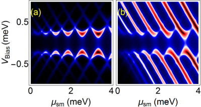
Consider now the dependence of the differential conductance of a short wire on the chemical potential and bias voltage as in Fig. 7. Here, and As shown in Fig. 7 (a), in the case of a “clean” parent superconductor the features are particle-hole symmetric and strongly suppressed at large bias voltages, as discussed in the context of Fig. 1. By contrast, a finite density of sub-gap states in the parent superconductor introduces particle-hole asymmetry, as shown in panel (b) of Fig. 7. Also note that the particle-hole asymmetric “stripy” features have similar slopes at positive and negative values of and are not suppressed at large bias voltages. These types of features are present in the experimentally measured differential conductance of SM-SC hybrid structuresChen et al. (2016), suggesting that parent superconductors such as NbTiN may have a non-vanishing density of sub-gap states.
We note that these results are consistent with the existence of some generic dissipationLiu et al. (2017). Here, we propose the presence of a small but finite density of sub-gap states in the parent superconductor as the natural mechanism responsible for dissipation effects. Thus, dissipation is just one among several important low-energy effects that are directly linked to the parent superconductor, which can be captured theoretically by explicitly incorporating the bulk SC into the modeling. Two relevant examples – the dependence of the quasiparticle spectral weight within the SM wire on the SM-SC coupling and the renormalization of the low-energy spectrum – are discussed below. Explicitly incorporating the parent SC into the theory provides a unified framework for describing these effects, which otherwise require different ad hoc ingredients. This suggests that a thorough investigation of the parent superconductor (in the presence of disorder and finite magnetic fields) is absolutely necessary for understanding in detail the low-energy physics of the hybrid structure.
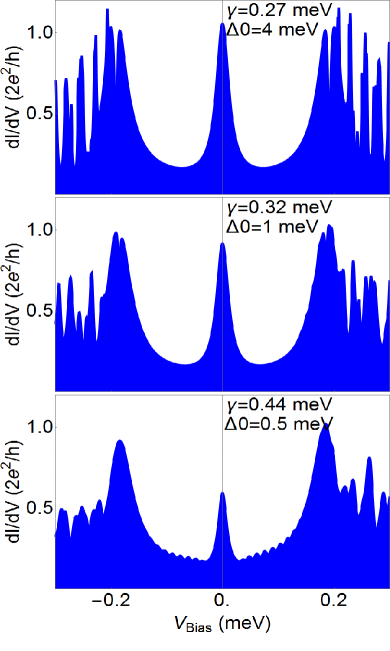
Figure 8 shows differential conductance curves in the topological regime for three different values of the ratio between the SM-SC coupling and the parent SC gap. The induced gap is kept constant. Notice that the height of the ZBP decreases with increasing . This dependence is the result of the dissipation effect generated by the non-vanishing density of subgap states in combination with the reduction of the spectral weight within the SM wire associated with the Majorana mode. More specifically, as the (relative) coupling strength increases, the spectral weight of the low-energy states (including the Majorana mode) is transfered from the SM wire to the parent SC.Stanescu and Sarma (2017) Consequently, for a given value of the tunnel barrier transparency, the weight of the corresponding differential conductance peak decreases as the coupling strength increases, as illustrated in Fig. 8. The shape of the ZBP will be studied in more detail in the next section.
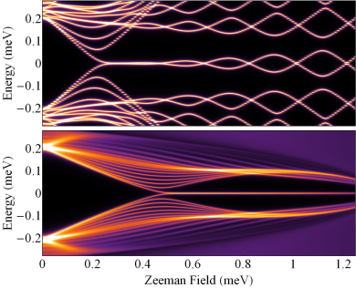
The dependence of the ZBP height on the coupling strength cannot be captured using an effective pairing potential model with an ad hoc dissipation term. To emphasize the importance of explicitly including the parent SC, we compare the dependence of the low-energy spectrum on the applied Zeeman field for i) a 1D wire with an effective pairing potential (model I) and ii) a 1D system that explicitly includes the parent SC (model II). The length of the SM wire is m and the SM-SC coupling strength is meV. To better simulate the experimental conditions, we assume that the bulk SC gap is suppressed by the applied magnetic field. Explicitly, we have , with meV and meV. The corresponding induced gap (defined as the minimum quasiparticle gap at zero field) isStanescu and Sarma (2017) meV. Since the induced gap is one of the most robust and experimentally accessible features, we consider an effective pairing model characterized by the same value of the induced gap and a field-dependent pairing of the form . Finally, we assume that the parent SC has sub-gap states corresponding to eV. A corresponding dissipation term is included in the effective pairing potential model. We expect to be strongly dependent on the applied magnetic field, but we do not incorporate this effect.
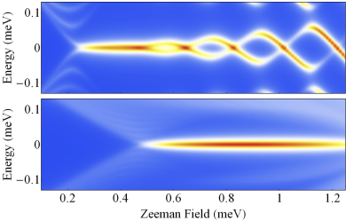
The dependence of the density of states within the wire on the Zeeman field is shown in Fig. 9, while the signature of the Majorana mode in the differential conductance is illustrated in Fig. 10. Several observations are warranted. First, the two models predict different values of the critical field corresponding to the emergence of the Majorana mode, despite the fact that they are characterized by the same value of the induced gap at . Indeed, assuming that the chemical potential is , the effective pairing approximation (model I) predicts a critical field given by the induced gap, , while incorporating the parent SC (model II) gives a critical field controlled by the SM-SC coupling strength,Stanescu and Sarma (2017) . Of course, one can construct effective pairing models that give the same value of the critical field as model II, but the corresponding quasiparticle gaps will be significantly overestimated in the intermediate and strong coupling regimes, i.e. for . Second, we note the strong energy renormalization that leads to the suppression of the Majorana splitting oscillations in model II. One can still have Majorana splitting in the intermediate/strong coupling regime, but it requires very short wires. Note that in model I the collapse of the SC gap at has no visible impact on the amplitude of the oscillations, which is increasing with the Zeeman field (see top panels in Figs. 9 and 10). On the other hand, in model II the collapse of the SC gap results in a reduction of the ZBP height. This is another manifestation of the dependence of the quasiparticle spectral weight on . Since is field-dependent, the relative SM-SC coupling strength increases with , which results in a decrease of the spectral weight of the Majorana mode reflected in the conductance. We emphasize that in these calculations the chemical potential is constant, hence the Fermi k-vector and the corresponding Fermi velocity of the Majorana band increase with the applied field. Consequently, the transparency of the barrier increases with . In model I, this results in a ZBP that becomes stronger with ; i.e., its weight increases with the field and so does its height (if it is below the quantized value at finite and/or ) whenever the wire is long-enough (to avoid energy splitting). In model II, on the other hand, the effect of a higher barrier transparency is offset by the loss of spectral weight, the net result being the eventual decrease of the ZBP strength upon approaching . Finally, we note that the dissipation-induced particle-hole asymmetry responsible for the “stripy” features in Fig. 7 is present even at very low energies, as illustrated in the top panel of Fig. 10. This effect could explain recent experimental observationsChen et al. (2016) showing similar low-energy features.
III.4 The shape of the zero bias conductance peak
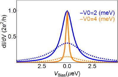
We conclude our analysis with a summary of the dependence of the Majorana-induced zero-bias conductance peak on the relevant system parameters. In this section we will study the ZBP of a hybrid system consisting of a very short nanowire of length m coupled to a superconductor with meV, the effective coupling strength being meV. The Zeeman field is set to meV. We note that having a short wire ensures that the Majorana mode is separated by a large gap from finite energy excitations, so that the area associated with the zero-bias conduction peak can be accurately estimated. Figure 11 shows the Majorana-induced zero-bias peak (ZBP) at for two different values of the potential barrier in a system with either a clean parent superconductor (solid lines) or a superconductor with a finite density of sub-gap states (dashed lines). First, we note that in the clean system the ZBPs are quantized at and that their widths (and, implicitly, the areas under the corresponding curves) are reduced by increasing the barrier potential (i.e., reducing the transparency of the barrier). Second, in the structure with a “dirty” parent superconductor (dashed lines in Fig. 11) the height of the ZBP is significantly lower than the quantized value. In fact, the effect of sub-gap states being present in the superconductor is to introduce a broadening of the Majorana mode. The area under the curve is the same as in the clean system (for a given potential barrier), but the width of the peak is intrinsically finite. In other words, increasing the barrier height generates a thin quantized peak in the clean system, but results in a small wide peak in the presence of sub-gap states (see solid and dashed orange/light gray lines in Fig. 11). Intuitively, we can understand the broadening of the ZBP as a result of the Majorana mode hybridizing with the sub-gap states from the parent superconductor. The resulting hybrid states will have energies distributed within a certain -dependent energy window about zero. As a result, the LDOS at the end of the wire will be characterized by a finite width peak centered at .Stanescu and Sarma (2017) By contrast, in a clean system the corresponding signature of the Majorana mode is a delta function-type contribution to the LDOS. Note that the broadening effect of the sub-gap states is qualitatively similar to the effect of finite temperature.
The dependence of the zero-bias conduction peak on the transparency of the barrier, temperature, and density of sub-gap states is shown in Fig. 12. First, we note that the transparency of the barrier depends on both the height and width of the barrier potential. For simplicity, we model the potential barrier as a Gaussian, . Hence, the height of the barrier is parametrized by and its width by the standard deviation . Increasing or reduces the transparency of the barrier, which results in a smaller area under the curve [see panel (a)]. Note that in a clean system at the height of the ZBP is quantized for all values of and . For a given tunnel barrier potential, introducing finite temperature or finite density of sub-gap states (in the parent SC) does not modify the area of the ZBP, but broadens the peak. Consequently, its height gets reduced. The dependence of the ZBP height on and for different potential barriers is shown in panels (b) and (c), respectively. Note the similarities between the dependence of the ZBP height on temperatureLin et al. (2012); Liu et al. (2017) (panel b) and on the density of subgap states (panel c).
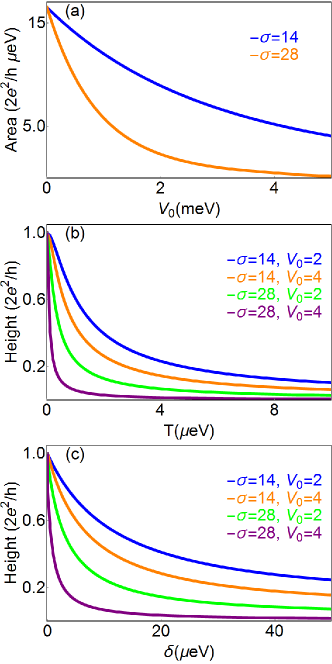
In the high temperature limit, which is barrier-dependent, see Fig. 12 (b), the dependence of the height of the ZBP on temperature is given by the analytical expression , where is the area of the ZBP. Similarly, in the limit of high density of sub-gap states, the dependence of the height of the ZBP on is given by . As the zero-bias peak approaches its quantized value with lowering (or ), the dependence of its height on temperature (or on the density of sub-gap states) becomes more complicated. We note that all the curves in panel (b) can be collapsed into a single curve corresponding to a ZBP of area through the scaling transformation , where is the area under the ZBP corresponding to an arbitrary curve. Similarly, any two curves in panel (c) are related to one another by the transformation and can be collapsed into a single curve. However, the transformation mapping a curve with area in panel (b) to a curve in panel (c) with the same area under the ZBP only works in the high-temperature/high density of sub-gap states regimes.
We note that all transport experiments on semiconductor-superconductor hybrid structures reported so far have observed zero-bias peaks having heights significantly smaller than the (theoretically predicted) quantized value, . These small values are inconsistent with expectations based on the nominal temperature of the system. Of course, the effective temperature could be much higher. However, the presence of sub-gap states is a natural alternative explanation for the low values of the observed zero-bias conduction peaks.
IV Conclusions
We have calculated the tunneling conductance of a normal metal - semiconductor wire - superconductor structure within the Blonder-Tinkham-Klapwijk and Keldysh formalisms by treating the parent superconductor as an active component of the hybrid system. This treatment ensures that several key effects that control the low-energy physics of the hybrid structure are accurately captured by the theory. These effects include the proximity-induced renormalization of the low-energy states, including the renormalization of the topological gap that protects the Majorana zero modes,Stanescu and Sarma (2017) the emergence of additional conductance peaks at energies corresponding to the gap edge of the parent superconductorCole et al. (2015); Reeg and Maslov (2017); Stanescu and Sarma (2017), and the broadening of the low-energy features due to hybridization of the states within the semiconductor wire with sub-gap states in the parent superconductorStanescu and Sarma (2017).
We find that the differential conductance is a good indicator for the local density of states at the end on the hybrid structure adjacent to the tunnel barrier. This includes both the semiconductor wire and the nearby parent superconductor. A clearly defined feature associated with the parent superconductor emerges at energies corresponding to the bulk gap. In the intermediate/strong coupling regime the features associated with sub-gap states (e.g., the induced gap) and those corresponding to contributions from the parent superconductor have similar characteristic energies. We predict that one can disentangle them by varying the strength of the potential barrier, which has a stronger effect on the sub-gap features. For example, in the high barrier limit one can almost completely suppress the sub-gap features while having a measurable parent superconductor contribution. In the topological regime, varying the transparency of the tunnel barrier changes the area of the zero-bias conductance peak, while its height is quantized () at zero temperature. Finite temperature reduces the height of the ZBP but preserves its area.
The most dramatic implication of treating the parent superconductor as an active component of the system occurs if we assume that the superconductor itself has sub-gap states induced by disorder and finite magnetic fields. These states hybridize with the low-energy states in the semiconductor wire significantly altering their properties. We find that in the presence of sub-gap states in the parent superconductor the differential conductance develops characteristic “stripy” features (as function of the chemical potential and bias voltage) that break particle-hole symmetry. In addition, the presence of sub-gap states has an effect similar to finite temperature and destroys the quantization of the Majorana-induced zero-bias conductance peak. More generally, the presence of these states results in a broadening of the low-energy features that characterize the hybrid structure. From the perspective of quantum computation, this is a deadly effect, as it destroys the topological gap that protects the low-energy Majorana subspace. All the signatures identified here as being associated with the presence of sub-gap states in the parent superconductor can be recognized in the transport measurements on semiconductor-superconductor hybrid structures reported so far. Therefore, we find it imperative to understand in detail the low-energy properties of currently-used parent superconductors, such as Al and NbTiN, and to consider a systematic effort to optimize their properties or to engineer better suited parent superconductors.
In summary, we have shown that explicitly treating the parent superconductor as an active component of the semiconductor-superconductor structure generates a number of features in the calculated differential tunneling conductance that would otherwise be absent. Some of these features have not been previously discussed in any detail. One of the new features is the reduction in weight of the differential conductance peaks as the coupling to the parent superconductor increases, as shown in Fig. 2. Since the reduction (and eventual collapse) of the parent SC gap at high magnetic fields implies an increase of the effective coupling (relative to the SC gap), a consequence of this feature is the decrease of the ZBP strength at high Zeeman fields, as illustrated in Fig. 10. Another feature is the presence of a superconducting resonance at the energy scale corresponding to the bulk gap (see Fig. 3) with an amplitude that has a dependence on the tunnel barrier height different from that of sub-gap (induced) peaks, as shown in Fig. 5. In addition, the possible presence of sub-gap states in the parent superconductor results in particle-hole asymmetric “stripy” features in the differential conductance, like those illustrated in Fig. 7, that persist even at very low energy, as shown in Fig. 10. Finally, explicitly considering the parent superconductor can strongly suppress the Majorana energy splitting oscillations and generate a finite density of states inside the topological gap, as shown in Fig. 10. Considering that all these features, some of them new, which were calculated within a unitary framework that explicitly incorporates the superconductor, have been observed experimentally in tunneling measurements on semiconductor-superconductor structures, we conclude that our work provides strong evidence regarding the critical role of the parent superconductor in Majorana devices.
This work is supported by NSF DMR-1414683.
References
- Hasan and Kane (2010) M. Z. Hasan and C. L. Kane, Rev. Mod. Phys. 82, 3045 (2010).
- Qi and Zhang (2011) X.-L. Qi and S.-C. Zhang, Rev. Mod. Phys. 83, 1057 (2011).
- Bernevig (2013) B. A. Bernevig, Topological Insulators and Topological Superconductors (Princeton University Press, New Jersey, 2013).
- Alicea (2012) J. Alicea, Reports on Progress in Physics 75, 076501 (2012).
- Leijnse and Flensberg (2012) M. Leijnse and K. Flensberg, Semiconductor Science and Technology 27, 124003 (2012).
- Beenakker (2013) C. Beenakker, Annual Review of Condensed Matter Physics 4, 113 (2013), http://dx.doi.org/10.1146/annurev-conmatphys-030212-184337 .
- Stanescu and Tewari (2013) T. D. Stanescu and S. Tewari, J. Phys.: Condens. Matter 25, 233201 (2013).
- Nayak et al. (2008) C. Nayak, S. H. Simon, A. Stern, M. Freedman, and S. Das Sarma, Rev. Mod. Phys. 80, 1083 (2008).
- Stanescu (2017) T. D. Stanescu, Introduction to topological quantum matter and quantum computation (CRC Press, Taylor & Francis Group, 2017).
- Lutchyn et al. (2010) R. M. Lutchyn, J. D. Sau, and S. Das Sarma, Phys. Rev. Lett. 105, 077001 (2010).
- Oreg et al. (2010) Y. Oreg, G. Refael, and F. von Oppen, Phys. Rev. Lett. 105, 177002 (2010).
- Read and Green (2000) N. Read and D. Green, Phys. Rev. B 61, 10267 (2000).
- Sau et al. (2010) J. D. Sau, S. Tewari, R. M. Lutchyn, T. D. Stanescu, and S. Das Sarma, Phys. Rev. B 82, 214509 (2010).
- Sengupta et al. (2001) K. Sengupta, I. Žutić, H.-J. Kwon, V. M. Yakovenko, and S. Das Sarma, Phys. Rev. B 63, 144531 (2001).
- Law et al. (2009) K. T. Law, P. A. Lee, and T. K. Ng, Phys. Rev. Lett. 103, 237001 (2009).
- Flensberg (2010) K. Flensberg, Phys. Rev. B 82, 180516 (2010).
- Wimmer et al. (2011) M. Wimmer, A. R. Akhmerov, J. P. Dahlhaus, and C. W. J. Beenakker, New Journal of Physics 13, 053016 (2011).
- Fidkowski et al. (2012) L. Fidkowski, J. Alicea, N. H. Lindner, R. M. Lutchyn, and M. P. A. Fisher, Phys. Rev. B 85, 245121 (2012).
- Mourik et al. (2012) V. Mourik, K. Zuo, S. M. Frolov, S. R. Plissard, E. P. A. M. Bakkers, and L. P. Kouwenhoven, Science 336, 1003 (2012).
- Deng et al. (2012) M. T. Deng, C. L. Yu, G. Y. Huang, M. Larsson, P. Caroff, and H. Q. Xu, Nano Letters 12, 6414 (2012).
- Das et al. (2012) A. Das, Y. Ronen, Y. Most, Y. Oreg, M. Heiblum, and H. Shtrikman, Nature Physics 8, 887 (2012).
- Finck et al. (2013) A. D. K. Finck, D. J. Van Harlingen, P. K. Mohseni, K. Jung, and X. Li, Phys. Rev. Lett. 110, 126406 (2013).
- Chang et al. (2015) W. Chang, S. M. Albrecht, T. S. Jespersen, F. Kuemmeth, P. Krogstrup, J. Nygård, and C. M. Marcus, Nat Nano 10, 232 (2015).
- Albrecht et al. (2016) S. M. Albrecht, A. P. Higginbotham, M. Madsen, F. Kuemmeth, T. S. Jespersen, J. Nygård, P. Krogstrup, and C. M. Marcus, Nature 531, 206 (2016).
- Zhang et al. (2016) H. Zhang, O. Gul, S. Conesa-Boj, K. Zuo, V. Mourik, F. K. de Vries, J. van Veen, D. J. van Woerkom, M. P. Nowak, M. Wimmer, D. Car, S. Plissard, E. P. A. M. Bakkers, M. Quintero-Pérez, S. Goswami, K. Watanabe, T. Taniguchi, and L. P. Kouwenhoven, e-print arXiv:1603.04069 (2016).
- Deng et al. (2016) M. T. Deng, S. Vaitiekenas, E. B. Hansen, J. Danon, M. Leijnse, K. Flensberg, J. Nygård, P. Krogstrup, and C. M. Marcus, Science 354, 1557 (2016).
- Chen et al. (2016) J. Chen, P. Yu, J. Stenger, M. Hocevar, D. Car, S. R. Plissard, E. P. Bakkers, T. D. Stanescu, and S. M. Frolov, e-print arXiv:1610.04555 (2016).
- Stanescu et al. (2011) T. D. Stanescu, R. M. Lutchyn, and S. Das Sarma, Phys. Rev. B 84, 144522 (2011).
- Pientka et al. (2012) F. Pientka, G. Kells, A. Romito, P. W. Brouwer, and F. von Oppen, Phys. Rev. Lett. 109, 227006 (2012).
- Prada et al. (2012) E. Prada, P. San-Jose, and R. Aguado, Phys. Rev. B 86, 180503 (2012).
- Lin et al. (2012) C.-H. Lin, J. D. Sau, and S. Das Sarma, Phys. Rev. B 86, 224511 (2012).
- Rainis et al. (2013) D. Rainis, L. Trifunovic, J. Klinovaja, and D. Loss, Phys. Rev. B 87, 024515 (2013).
- Stanescu et al. (2014) T. D. Stanescu, R. M. Lutchyn, and S. Das Sarma, Phys. Rev. B 90, 085302 (2014).
- Yan and Wan (2014) Z. Yan and S. Wan, New Journal of Physics 16, 093004 (2014).
- Setiawan et al. (2015) F. Setiawan, P. M. R. Brydon, J. D. Sau, and S. Das Sarma, Phys. Rev. B 91, 214513 (2015).
- Liu et al. (2017) C.-X. Liu, J. D. Sau, and S. Das Sarma, Phys. Rev. B 95, 054502 (2017).
- Peng et al. (2015) Y. Peng, F. Pientka, Y. Vinkler-Aviv, L. I. Glazman, and F. von Oppen, Phys. Rev. Lett. 115, 266804 (2015).
- Sharma and Tewari (2016) G. Sharma and S. Tewari, Phys. Rev. B 93, 195161 (2016).
- Chevallier and Klinovaja (2016) D. Chevallier and J. Klinovaja, Phys. Rev. B 94, 035417 (2016).
- Setiawan et al. (2017) F. Setiawan, W. S. Cole, J. D. Sau, and S. Das Sarma, Phys. Rev. B 95, 020501 (2017).
- Reeg and Maslov (2017) C. Reeg and D. L. Maslov, Phys. Rev. B 95, 205439 (2017).
- Stanescu and Sarma (2017) T. D. Stanescu and S. D. Sarma, e-print arXiv:1702.03976 (2017).
- Blonder et al. (1982) G. E. Blonder, M. Tinkham, and T. M. Klapwijk, Phys. Rev. B 25, 4515 (1982).
- Rammer and Smith (1986) J. Rammer and H. Smith, Rev. Mod. Phys. 58, 323 (1986).
- Sticlet et al. (2016) D. Sticlet, B. Nijholt, and A. Akhmerov, e-print arXiv:1609.00637 (2016).
- Berthod and Giamarchi (2011) C. Berthod and T. Giamarchi, Phys. Rev. B 84, 155414 (2011).
- He et al. (2014) J. J. He, T. K. Ng, P. A. Lee, and K. T. Law, Phys. Rev. Lett. 112, 037001 (2014).
- Cole et al. (2015) W. S. Cole, S. Das Sarma, and T. D. Stanescu, Phys. Rev. B 92, 174511 (2015).
- Cole et al. (2016) W. S. Cole, J. D. Sau, and S. Das Sarma, Phys. Rev. B 94, 140505 (2016).
- Hui et al. (2015) H.-Y. Hui, J. D. Sau, and S. Das Sarma, Phys. Rev. B 92, 174512 (2015).
- Martin and Mozyrsky (2014) I. Martin and D. Mozyrsky, Phys. Rev. B 90, 100508 (2014).
- Bauriedl et al. (1981) W. Bauriedl, P. Ziemann, and W. Buckel, Phys. Rev. Lett. 47, 1163 (1981).
- Yazdani et al. (1997) A. Yazdani, B. A. Jones, C. P. Lutz, M. F. Crommie, and D. M. Eigler, Science 275, 1767 (1997), http://science.sciencemag.org/content/275/5307/1767.full.pdf .
- Das Sarma et al. (2016) S. Das Sarma, A. Nag, and J. D. Sau, Phys. Rev. B 94, 035143 (2016).