Computing in Memory with Spin-Transfer Torque Magnetic RAM ††thanks: This work was supported in part by STARnet, a Semiconductor Research Corporation program sponsored by MARCO and DARPA, and in part by National Science Foundation under grant 1320808.
Abstract
In-memory computing is a promising approach to addressing the processor-memory data transfer bottleneck in computing systems. We propose Spin-Transfer Torque Compute-in-Memory (STT-CiM), a design for in-memory computing with Spin-Transfer Torque Magnetic RAM (STT-MRAM). The unique properties of spintronic memory allow multiple wordlines within an array to be simultaneously enabled, opening up the possibility of directly sensing functions of the values stored in multiple rows using a single access. We propose modifications to STT-MRAM peripheral circuits that leverage this principle to perform logic, arithmetic and complex vector operations. We address the challenge of reliable in-memory computing under process variations by extending ECC schemes to detect and correct errors that occur during CiM operations. We also address the question of how STT-CiM should be integrated within a general-purpose computing system. To this end, we propose architectural enhancements to processor instruction sets and on-chip buses that enable STT-CiM to be utilized as a scratchpad memory. Finally, we present data mapping techniques to increase the effectiveness of STT-CiM. We evaluate STT-CiM using a device-to-architecture modeling framework, and integrate cycle-accurate models of STT-CiM with a commercial processor and on-chip bus (Nios II and Avalon from Intel). Our system-level evaluation shows that STT-CiM provides system-level performance improvements of 3.93x on average (upto 10.4x), and concurrently reduces memory system energy by 3.83x on average (upto 12.4x).
Index Terms:
STT-MRAM, Processing-in-Memory, In-memory Computing, Spintronic MemoriesI Introduction
The growth in data processed and increase in the number of cores place high demands on the memory systems of modern computing platforms. Consequently, a growing fraction of transistors, area and power are utilized towards memories. CMOS memories (SRAM and embedded DRAM) have been the mainstays of memory design for the past several decades. However, recent technology scaling challenges in CMOS memories, along with an increased demand for memory capacity and performance, have fueled an active interest in alternative memory technologies.
Spintronic memories have emerged as a promising candidate for future memories due to several desirable attributes such as non-volatility, high density, and near-zero leakage. In particular, Spin Transfer Torque Magnetic RAM (STT-MRAM) has garnered significant interest with various prototype demonstrations and early commercial offerings [everspin, grandis, avalanche]. There have been several research efforts to boost the efficiency of STT-MRAM at the device, circuit and architectural levels [jog_dac, early_write, saibal_stt, yusung_stt, toshiba_1, partial_line, smullen_hpca, stt_llc, konWoo_yield_stt, umn_ecc, wangECC, STT_yield_wang, xfong_failure, mtj_20nm, approx_storage, 3d_stt, lee_esttmram, stt_universal, hca_jadidi, multi_zhang, hmt_jishen, stt_trans_sizing, sttcache_siabal, coast, ikeda2008, wangRecofigSTTMRAM, dualpillar]. In this work, we explore viz in-memory computing with STT-MRAM. By exploiting the ability to simultaneously enable multiple wordlines within a memory array, we enhance STT-MRAM arrays to perform a range of arithmetic, logic and vector operations. We propose circuit and architectural techniques for reliable computation under process variations and to enable the proposed design to be used in a programmable processor based system.
In-memory computing is motivated by the observation that the movement of data from bit-cells in the memory to the processor and back (across the bit-lines, memory interface, and system interconnect) is a major performance and energy bottleneck in computing systems. Efforts that have explored the closer integration of logic and memory are variedly referred to in the literature as logic-in-memory, computing-in-memory and processing-in-memory. These efforts may be classified into two categories – moving logic closer to memory, or near-memory computing [iram, activepages, activedisks, diva, active_memory_cube, nmc_article, neurocube, nda, ndc, toppim, pim_enabled, interpolation_mem, hmc, hbm], and performing computations within memory structures, or in-memory computing [tcam, compute_mem_sad, UMN_CRAM, pinatubo, MAGIC, memristiveLogic, bulk_bitwise2, acdimm, wangLiM, verma, reno, spindle, prime], which is the focus of this work. In-memory computing reduces the number of memory accesses and the amount of data transferred between processor and memory, and exploits the wider internal bandwidth available within memory systems.
Our proposal is based on the observation that by enabling multiple wordlines simultaneously 111Note that this is much easier in STT-MRAM than in CMOS memories, due to the resistive nature of the bit-cells. and sensing the effective resistance of each bit-line, it is possible to directly compute logic functions of the values stored in the bit-cells. Based on this insight, we propose STT-CiM, a design for in-memory computing with STT-MRAM that can perform a range of arithmetic, logic, and vector operations. In STT-CiM, the core data array is the same as standard STT-MRAM; hence, memory density and the efficiency of read and write operations are maintained. Reliable sensing under the limited tunneling magneto-resistance (TMR) of STT-MRAM bit-cells is known to be a challenge [konWoo_yield_stt, umn_ecc, STT_yield_wang, xfong_failure, wangECC, wangRecofigSTTMRAM], and we show that challenge this is further aggravated for in-memory computations. In order to enhance the robustness of STT-CiM under process variations, we extend error correction codes (ECC) to errors that occur during in-memory computations. To evaluate the benefits of STT-CiM, we utilize it as a scratchpad in the memory hierarchy of the Intel Nios II [nios2] processor. We propose enhancements to the on-chip bus and extend the instruction set of the processor to support compute-in-memory operations and expose them to software. We also present suitable data mapping techniques to maximize the benefits of STT-CiM.
We note that earlier efforts (e.g., [pinatubo]) have proposed enabling multiple wordlines to perform computations within Non-Volatile Memories (NVMs). Although our work shares this principle, we differ from previous work in several key aspects: (i) we address reliable in-memory computing under process variations, (ii) we go beyond bitwise logic operations to also perform arithmetic and vector operations, which are commonly present in modern computing workloads, and (iii) we propose architectural enhancements (bus and ISA extensions), and data mapping techniques to enable in-memory computation in the context of on-chip scratchpad memories.
In summary, the key contributions of this work are as follows:
-
•
We explore compute-in-memory with spintronic memories as an approach to improving system performance and energy.
-
•
We propose STT-CiM, an enhanced STT-MRAM array that can perform a range of arithmetic, logic and vector compute-in-memory operations without modifying either the bit-cells or the core data array.
-
•
We address a key challenge in STT-CiM, i.e. reliably performing in-memory operations under process variation, by demonstrating suitable error correction mechanisms.
-
•
We propose extensions to the instruction set and on-chip bus to integrate STT-CiM into a programmable processor system and demonstrate the viability of these extensions using Intel’s Nios II processor and Avalon on-chip bus.
-
•
We evaluate the performance and energy benefits of STT-CiM, achieving average improvements of 3.83x (upto 12.4x) and 3.93x (upto 10.4x) in the total memory energy and system performance, respectively.
The rest of the paper is organized as follows. Section II presents an overview of prior research efforts related to in-memory computation. Section III provides the necessary background on STT-MRAM. Section IV describes the STT-CiM design and how it supports in-memory computation. Section LABEL:sec:lim_architecture outlines architectural enhancements for STT-CiM. Section LABEL:sec:exptsetup describes the experimental methodology and experimental results are presented in section LABEL:sec:results. Section LABEL:sec:conclusion concludes the paper.
II Related Work
The closer integration of logic and memory is variedly referred to in the literature as logic-in-memory, computing-in-memory, and processing-in-memory. These efforts can be broadly classified into two categories, as shown in Figure 1. We limit the scope of our discussion to approaches that improve the efficiency of active computation. For example, we do not discuss the embedding of non-volatile memory elements into a logic circuit [hanyu_lim_challenges, non_volatile_processor, matsunaga_prospects, meng_chang] in order to enable the system to shut-down and wakeup efficiently for improved power management.
Near-memory computing refers to bringing logic or processing units closer to memory. Notwithstanding the closer integration, processing units still remain distinct from memory arrays. Near-memory computing has been explored at various levels of the memory hierarchy [iram, activepages, activedisks, diva, active_memory_cube, neurocube, nda, ndc, toppim, pim_enabled, interpolation_mem, hmc, hbm]. Intelligent RAM (IRAM) [iram] is an early example, which integrated a processor and DRAM in the same chip to improve the bandwidth between them. Embedding simple processing units within each page of main memory [activepages] and within secondary storage [activedisks] enables computations to be performed near memory. An application-specific example of near-memory computation is memory that can generate interpolated values, enabling the evaluation of complex mathematical functions [interpolation_mem]. Near-memory computing has gained significant interest in recent years, with industry efforts like Hybrid Memory Cube (HMC) [hmc] and High Bandwidth Memory (HBM) [hbm].
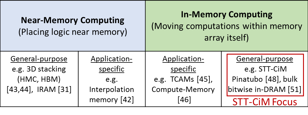
In-memory computing [tcam, compute_mem_sad, UMN_CRAM, pinatubo, bulk_bitwise2, acdimm, verma, wangLiM] integrates logic operations into memory arrays, fundamentally blurring the distinction between processing and memory. The key challenge of in-memory computing is to realize it without impacting the desirability of the resulting design as a standard memory (i.e., density or efficiency of standard read and write operations). Due to these constraints, in-memory computing is typically limited to performing a small number of simple operations.
We can classify previous proposals for in-memory computing based on whether they target application-specific or general-purpose computations, and based on the underlying memory technology that they consider. Application-specific examples of in-memory computing include vector-matrix multiplication [verma, reno, spindle, prime] and sum-of-absolute difference [compute_mem_sad] computation. Ternary content-addressable memory [tcam], ROM-embedded RAM [rom_embedded_ram], AC-DIMM [acdimm] and Micron’s automata processor [micron_ap] can also be viewed as examples of in-memory computing that target specific operations such as pattern matching or evaluation of transcendental functions. Unlike these application-specific designs, we focus on embedding a broader set of operations (arithmetic, logic and vector operations) within memory.
In-memory evaluation of bitwise logic operations has been explored for memristive memories [pinatubo, memristiveLogic, MAGIC] and DRAM [bulk_bitwise2]. Our work differs from these efforts in several important aspects. First, we focus on in-memory computing for spintronic memory, which involves fundamentally different prospects and design challenges. For example, the proposed operations are not destructive to the contents stored in the accessed bit-cells (unlike [bulk_bitwise2]). On the other hand, the much lower ratio of on to off resistance in spintronic memory leads to lower sensing margins. Second, we use a different sensing and reference generation circuitry, which enables us to natively realize a wider variety of operations. For example, the proposed design requires only one array access (unlike two in the case of [pinatubo]) to perform bit-wise XOR operations. Second, our design goes beyond bitwise logic operations and realizes arithmetic as well as complex vector operations. Third, we propose architectural extensions (bus and ISA extensions) and data mapping techniques to enable in-memory computing within a general-purpose processor system. Finally, we address a key challenge associated with in-memory computing, viz., reliable operation under process variations.
A different approach to in-memory computing with spintronic memories [UMN_CRAM] uses an extra transistor in each bit-cell (2T-1R cells), which sacrifices the density benefits of standard (1T-1R) STT-MRAM, while potentially enabling more complex functions to be evaluated within the array. In contrast, our proposal enables in-memory computation within a standard STT-MRAM array with no changes to the bit-cells. We note that a concurrent effort [wangLiM] has explored bit-wise AND/OR operations in STT-MRAM. The bit wise XOR operation cannot be realized atomically using the design proposed in [wangLiM]). Furthermore, these efforts restrict themselves to device and circuit level considerations, and do not address the architectural challenges of in-memory computing.
III Background
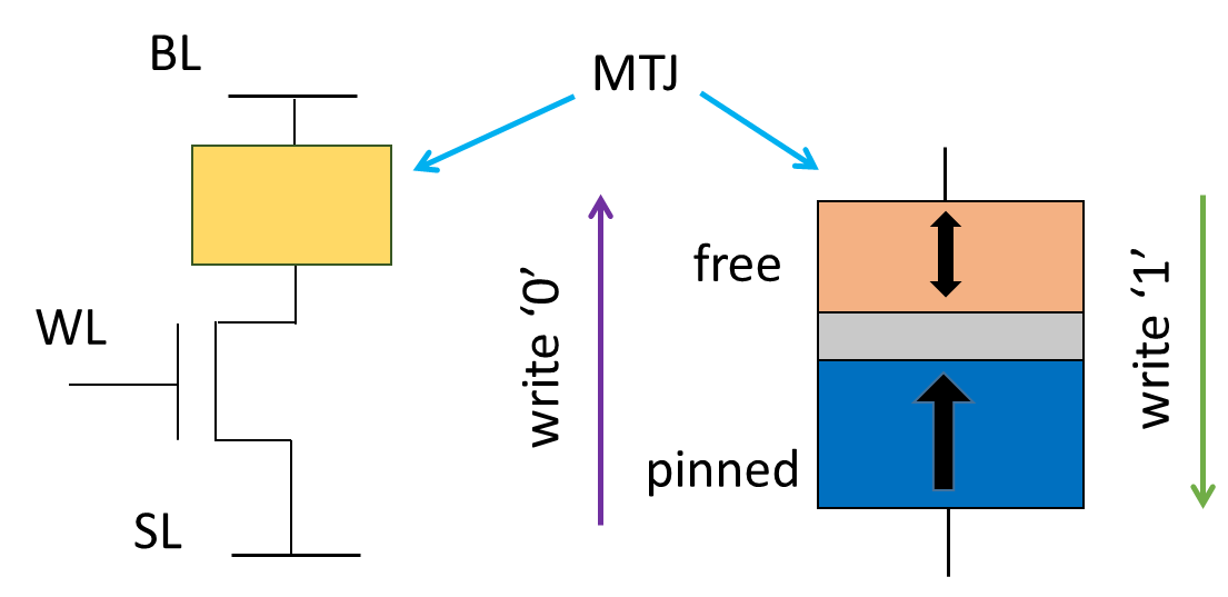
An STT-MRAM bit-cell consists of an access transistor and a magnetic tunnel junction (MTJ), as shown in Figure 2. An MTJ in turn consists of a pinned layer that has a fixed magnetic orientation and a free layer whose magnetic orientation can be switched. The magnetic layers are separated by a tunnelling oxide. The relative magnetic orientation of the free and pinned layers determines the resistance offered by the MTJ (the resistance for the parallel configuration, , is lower than the anti-parallel resistance, ). The two resistance states encode a bit (we assume that parallel represents logic “1”, and anti-parallel represents logic “0”). A read operation is performed by applying a bias () between the bitline (BL) and the source line (SL), and enabling the wordline (WL). The resultant current flowing through the bit-cell ( or ) is compared against a global reference to determine the logic state stored in the bit-cell.
A write is performed by passing a current greater than the critical switching current of the MTJ through the bit-cell. The logic value written is dependent on the direction of the write current as shown in Figure 2. The write operation in STT-MRAM is stochastic in nature, and the duration and magnitude of the write current determines the write failure rate. Apart from write failures, STT-MRAMs are also subject to read decision failures, where the value stored in a bit-cell is incorrectly sensed due to process variations, and read disturb failures where a read operation inadvertently ends up writing into the bit-cell. These failures are addressed through a range of techniques including device and circuit optimization, manufacturing test and self-repair, and error correcting codes [konWoo_yield_stt, umn_ecc, STT_yield_wang, xfong_failure]. Apart from write/read failures, memories may also have failures due to thermal noise, which causes stochastic flipping in the bit-cells. However, such failures are negligible in STT-MRAM due to the high energy barrier between the two resistance states.
IV STT-MRAM based Compute-in-Memory (STT-CiM)
In this section, we describe STT-MRAM based Compute-in-Memory (STT-CiM), a design for in-memory computing using standard STT-MRAM arrays.
IV-A STT-CiM overview
The key idea behind STT-CiM is to enable multiple wordlines simultaneously in an STT-MRAM array, leading to multiple bit-cells being connected to each bitline. With enhancements that we propose to the sensing and reference generation circuitry, we can directly compute logic functions of the enabled words. Note that such an operation is feasible in STT-MRAMs since the bit-cells are resistive, and since the write currents are typically much higher than read currents. In contrast, enabling multiple wordlines in SRAM can lead to short-circuit paths through the memory array, leading to loss of data stored in the bit-cells.
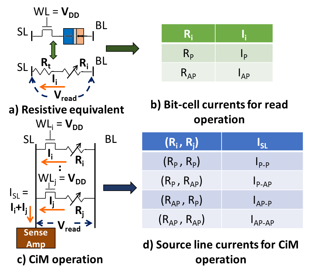
Figure 3 explains the principle of operation of STT-CiM. First, consider the resistive equivalent circuit of a single STT-MRAM bit-cell shown in Figure 3(a). represents the on-resistance of the access transistor and the resistance of the MTJ. When a voltage is applied between the bitline (BL) and the source line (SL), the net current flowing through the bit-cell can take two possible values depending on the MTJ configuration, as shown in Figure 3(b). A read operation involves using a sensing mechanism to distinguish between these two current values.
Figure 3(c) demonstrates a Compute-in-Memory (CiM) operation, where two wordlines ( and ) are enabled, and a voltage bias () is applied to the bitline. The resultant current flowing through the SL (denoted ) is a summation of the currents flowing through each of the bit-cells ( and ), which in turn depends on the logic states stored in these bit-cells. The possible values of are shown in Figure 3(d). We propose enhanced sensing mechanisms to distinguish between these values and thereby compute logic functions of the values stored in the enabled bit-cells. We discuss the details of these operations in turn below.
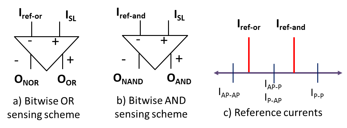
Bitwise OR (NOR). In order to realize logic OR and NOR operations, we use the sensing scheme shown in Figure 4(a), where is connected to the positive input of the sense amplifier and a reference current is fed to its negative input. We choose to be between and , as shown in Figure 4(c). As a result, among the possible values of [Figure 3(d)], only = is less than . Consequently, only the case where both bit-cells are in the AP configuration, i.e., both store “0”, leads to an output of logic “0” (“1”) at the positive (negative) output of the sense amplifier, while all other cases lead to logic “1” (“0”). Thus, the positive and negative outputs of the sense amplifier evaluate the logic OR and NOR of the values stored in the enabled bit-cells.
Bitwise AND (NAND). A bitwise AND (NAND) operation is realized at the positive (negative) terminal of the sense amplifier by using the sensing scheme shown in Figure 4(b). Note that in this scheme, a different reference current () is fed to the sense amplifier.
Bitwise XOR. A bitwise XOR operation is realized when the two sensing schemes shown in Figure 4 are used in tandem, and and are fed to a CMOS NOR gate. In other words, = NOR .
Table LABEL:tab:cim_sensing summarizes the logic operations achieved using the two sensing schemes discussed above. Note that, all the logic operations described above are symmetric in nature, and hence it is not necessary to distinguish between the cases where the two bit-cells connected to a bitline store “10” and “01”.