Nanostructured graphene for spintronics
Abstract
Zigzag edges of the honeycomb structure of graphene exhibit magnetic polarization making them attractive as building blocks for spintronic devices. Here, we show that devices with zigzag edged triangular antidots perform essential spintronic functionalities, such as spatial spin-splitting or spin filtering of unpolarized incoming currents. Near-perfect performance can be obtained with optimized structures. The device performance is robust against substantial disorder. The gate-voltage dependence of transverse resistance is qualitatively different for spin-polarized and spin-unpolarized devices, and can be used as a diagnostic tool. Importantly, the suggested devices are feasible within current technologies.
pacs:
73.21.Ac, 73.21.Cd, 72.80.VpIntroduction. The weak intrinsic spin-orbit coupling and long spin diffusion lengths suggest graphene as an ideal spintronic material Castro Neto et al. (2009); Han et al. (2010); Yazyev (2010); Nair et al. (2012); McCreary et al. (2012); Hong et al. (2012); Nair et al. (2013); Han et al. (2014); Tuan et al. (2014); Kamalakar et al. (2015). Spin splitting or filtering in graphene is predicted for half-metallic nanoribbons Son et al. (2006); Han et al. (2010); Ozaki et al. (2010); Saffarzadeh and Farghadan (2011), modulated Rashba fields Diniz et al. (2017), flakes Sheng et al. (2010), chains Zeng et al. (2010), or via the spin Hall effect (SHE) Kane and Mele (2005); Abanin et al. (2006); Balakrishnan et al. (2014); Cresti et al. (2014); Sinova et al. (2015). Half-metallic systems are excellent platforms for manipulating spin due to their inherent spin filtering behavior. Self-assembled organometallic frameworks Hu et al. (2014) and graphene-boron-nitride structures Pruneda (2010), point defects and hydrogenation Yazyev and Helm (2007); Palacios et al. (2008); Leconte et al. (2011), and, in particular, nanostructured zigzag (zz)-edged devices Son et al. (2006); Wimmer et al. (2008); Wang et al. (2009); Zheng et al. (2009); Ozaki et al. (2010); Sheng et al. (2010); Zeng et al. (2010); Saffarzadeh and Farghadan (2011); Potasz et al. (2012); Hong et al. (2016); Khan et al. (2016); Gregersen et al. (2016) are among the proposed graphene-based half metals. Spin filters have been proposed using triangular dots Sheng et al. (2010); Hong et al. (2016) or perforations Zheng et al. (2009) with many similarities, e.g., low-energy localized magnetic states and a net sublattice imbalance. However, perforations, or antidots Pedersen et al. (2008); Petersen et al. (2011); Ouyang et al. (2011), have the advantage over dots of being embedded in the graphene sheet which allows a wide range of spin-dependent transport properties. Although signatures of localized magnetic states have been detectedTao et al. (2011); Hashimoto et al. (2014); Magda et al. (2014), spin manipulation in graphene-based half metals has yet to be realized in experiments.
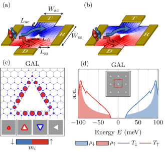
In this Rapid Communication, we investigate the transport properties of graphene devices with embedded zz-edged triangular antidots. Such devices are within the reach of state-of-the-art lithographic methods: Triangular holes in graphene have recently been fabricated Auton et al. (2016), and experiments suggest the possibility of zz-etched nanostructures Shi et al. (2011); Oberhuber et al. (2013). Another possibility is to employ a lithographic mask of patterned hexagonal boron nitride, which naturally etches into zz-edged triangular holes Jin et al. (2009); Gilbert et al. (2017). The zz-edged structures support local ferromagnetic moments Yazyev (2010), however, global ferromagnetism is induced when the overall sublattice symmetry of the edges is broken Son et al. (2006); Wimmer et al. (2008); Wang et al. (2009); Güçlü et al. (2010); Ozaki et al. (2010); Zeng et al. (2010); Saffarzadeh and Farghadan (2011). This occurs for zz-edged triangles Zheng et al. (2009); Sheng et al. (2010); Potasz et al. (2012); Hong et al. (2016); Khan et al. (2016); Gregersen et al. (2016). We have recently discussed the electronic structure of triangular graphene antidot lattices (GALs) Gregersen et al. (2016)—–here, we focus on transport through devices containing a small number of antidots. Our calculations show that large spin-polarized currents are generated by the device illustrated in LABEL:fig:scheme. An unpolarized current incident from the left is funneled below the triangle if the electron spin is up (, red) and above if the spin is down (, blue), resulting in spin-polarized currents at contacts top (T) and bottom (B), respectively.
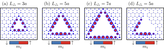
The sixfold symmetry of the graphene lattice allows only two orientations for zz-edged triangles. A rotation exposes zz edges with magnetic moments of opposite sign. In turn, this inverts both the scattering directions and spin polarization simultaneously. An independent inversion of either scattering direction or spin polarization would change the direction of spin current flow, but inverting both restores the spin current flow pattern [LABEL:fig:scheme.R]. This results in robust spin behavior over a wide range of superlattice geometries. The zz-edged triangular GALs have magnetic moment distributions as shown in LABEL:fig:moments, and display half-metallic behavior over a wide range of energies near the Dirac point. The roles of the two spin orientations can be interchanged by gating, as shown in LABEL:fig:dos. The magnetic profile remains qualitatively similar when the side length is varied [insets of LABEL:fig:moments], changes sign under a rotation, and magnetism vanishes for the rotated (armchair-edged) triangular antidot.
In analogy to (inverse) spin Hall measurements Sinova et al. (2015), we study the transverse resistance generated by a longitudinal current. Using a spin-polarized left contact we suggest a method to distinguish between magnetic or non-magnetic antidots in such devices: The transverse resistance has a characteristic antisymmetric behavior with respect to the Fermi level only for spin-polarized antidots.
Geometry and model. The device in LABEL:fig:scheme consists of a central graphene region with a single triangular antidot. (Below we also consider a larger central region with an array of triangles.) The device has four arms which terminate at metallic contacts—left (L), right (R), top (T), and bottom (B)—which act as sources of either unpolarized or single spin-orientation electrons. The triangular antidots here have a side length , where the lattice constant . The remaining dimensions in LABEL:fig:scheme are given in the caption. Our previous work Gregersen et al. (2016) validates the use of a nearest-neighbor tight-binding Hamiltonian , to describe the electronic structure of such systems, where () is a creation (annihilation) operator for an electron with spin on site . The hopping parameter is for neighbors and , and zero otherwise. The T and B arm widths are chosen to yield metallic behavior near the Fermi level .
Local magnetic moments are included via spin-dependent on-site energy terms , with for and for . The on-site magnetic moments , where is the number operator, are calculated from a self-consistent solution of the Hubbard model within the mean-field approximation. This is performed for the corresponding extended GAL, displayed in the inset of LABEL:fig:dos, which is an approximately square lattice with a () unit cell. The four short graphene arm segments are assumed to be nonmagnetic in order to isolate the magnetic influence of the antidots. An on-site Hubbard parameter gives results in good agreement with ab initio calculations in the case of graphene nanoribbons Yazyev (2010). The sublattice-dependent alignment of moments agrees with Ruderman-Kittel-Kasuya-Yosida (RKKY) theory predictions Saremi (2007); Power and Ferreira (2013). Our calculations assume that this extends to inter triangle alignments also. Due to the large total moment at each triangle, the inter triangle couplings should be stronger than those between, e.g., vacancy defects with similar separations.
The transmission for spin between two leads and and local (bond) currents from lead are calculated using recursive Green’s function techniques Lewenkopf and Mucciolo (2013). They are and , respectively. () is the retarded (advanced) Green’s function, is the broadening for lead , is the self-energy, and and are indices of neighboring sites. The spin and charge transmissions and local currents are defined for independent spin channels as , , , and , respectively. The metallic leads are included via an effective self-energy added to the edge sites of the metal/graphene interfaces Bahamon et al. (2013). For spin-polarized contacts, the self-energy for one spin channel is set to zero. The four-terminal transverse resistance is determined using L and R as the source and drain and T and B as voltage probes,
| (1) |
where the transverse potential drop . Using the Landauer-Büttiker relation, the charge currents through lead are . It is assumed that spin mixing occurs in the T and B leads, yielding spin-unpolarized potentials and . We apply source and drain potentials and , while T and B probes carry zero current, . The resistance is then determined by solving for , , and the longitudinal current.
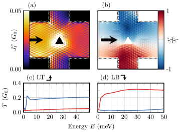
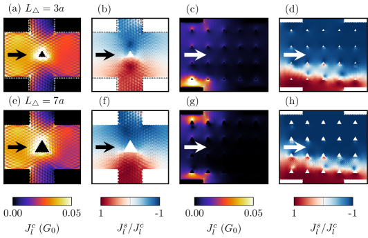
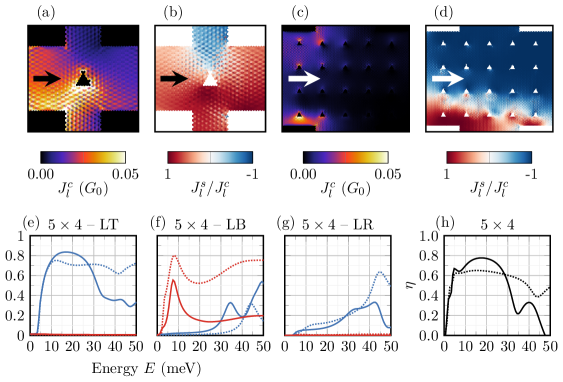
Results and discussion. Transport properties of the system in LABEL:fig:scheme are presented in Fig. 2. The spatial spin separation is illustrated by the magnitude of the local charge current and its spin polarization at , in LABEL:fig:1x1transport.currents.charge and LABEL:fig:1x1transport.currents.spin respectively. At this energy, electrons are channeled above the antidot and electrons below it. Incoming electrons are backscattered near the top vertex of the triangular antidot. This -electron behavior is also seen for both spins in the unpolarized system, i.e., letting all (not shown), and is due to geometrical factors: The jagged top half of the device is a more effective backscatterer in general than the nanoribbonlike bottom half. Conversely, the behavior is the opposite Backscattering occurs in the lower half of the device. This behavior is indicative of scattering near the bottom edge of the triangle which only occurs for electrons. This is supported by the presence of strong local density of states (DOS) features at the middle of each edge in the corresponding bulk lattice Gregersen et al. (2016). Therefore, the scattering of electrons is dictated mainly by the triangular shape of the antidot, whereas electrons are more sensitive to the magnetic profile. The L-T and L-B transmissions shown in LABEL:fig:1x1transport.LT and LABEL:fig:1x1transport.LB reveal that the spin polarization occurs for a broad range of energies. Thus, a single-antidot device can partially split or filter incoming currents into either T or B with a large degree of polarizations .
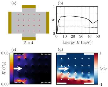
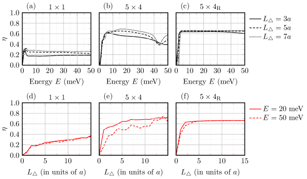
A array of triangular antidots is shown in LABEL:fig:5x4.scheme. We first assume that the magnetic moment profile is the same for each antidot [illustrated in LABEL:fig:5x4.scheme by red triangles] but below we relax this assumption. The electronic splitting of the spin currents can be quantified by an effective figure of merit
| (2) |
where for perfect spatial spin splitting into T and B. The figure of merit in LABEL:fig:5x4transport.efficiency is larger for the array (solid line) than for the single-antidot device (dotted line), further illustrated by the charge and spin currents at in LABEL:fig:5x4transport.currents.charge and LABEL:fig:5x4transport.currents.spin. The electrons are effectively blocked away from the array because of half metallicity at this energy, and are either backscattered, or directed towards the B contact. The electrons, on the other hand, may enter the array, but have a large probability of deflection towards the T contact due to repeated scattering of the type discussed for the single-antidot case. Thus, a large imbalance between the spin-resolved transmissions develops, with T and B polarizations around , and is enhanced.
The behavior is similar to the ratchet effect previously noted for triangular perturbations in graphene Koniakhin (2014). The spatial spin splitting shown here is somewhat analogous to the SHE Kane and Mele (2005); Abanin et al. (2006); Balakrishnan et al. (2014); Cresti et al. (2014); Sinova et al. (2015), where currents of opposite spin are pushed to the opposite edges of the device. A key distinction is that our device does not require spin-orbit coupling, or topologically protected transport channels. Even though the antidots share many similarities with regular dots, the enhanced spin splitting by repeated scattering from different antidots is difficult to envision in a dot-based system.
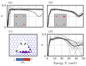
In experiments, disorder severely degrades properties of atomically precise antidot lattices Power and Jauho (2014). The half metallicity of triangular GALs is unusually robust against lattice disorder Gregersen et al. (2016). In Fig. 4, we study the effect of disorder in a antidot array using three different methods and ten realizations of each disorder type.
The first disorder type is a random flip of individual antidots, as illustrated in the inset of LABEL:fig:5x4dtransport.dF. The individual (gray solid) and averaged (black solid) figures of merit for this disorder [LABEL:fig:5x4dtransport.dF] are of the same order as the pristine array (black dashed). This is expected as the standard and flipped single-triangle devices display very similar behavior [LABEL:fig:scheme and LABEL:fig:scheme.R]. For comparison, for the case where every second antidot has been flipped [ (black dotted)], the efficiency is almost exactly identical to the disordered average. The spread of the different disorder realizations (gray curves) is very small, suggesting that the orientation of the individual antidots plays only a very minor role in these devices, and may even improve the figure of merit compared to the lattice of aligned antidots.
The second disorder type [inset of LABEL:fig:5x4dtransport.dL] randomly varies the triangle side lengths , where . The individual and the averaged splitting efficiencies are shown in LABEL:fig:5x4dtransport.dL. The effect of this disorder is minimal, suggesting that it is the presence of multiple spin-dependent scatterers with similar qualitative behavior and not their exact positioning or size, which enhances the spin-splitting effect. Enlarging or shrinking a triangle changes the length of the spin-polarized zz edge, and thus the total magnetic moment of an individual triangle [see the inset of LABEL:fig:moments, and the Supplemental Material 111See Supplemental Material [appended] for magnetic and transport properties of triangular antidots when varying side length and introducing edge disorder.]. However, the qualitative scattering processes are unchanged.
The third type of disorder, in LABEL:fig:5x4dtransport.dE.scheme, randomly removes edge atoms. Removing an edge atom splits the zz edges into smaller segments and significantly influences the magnetic moment profile (see also the Supplemental Material Note (1)). Random flipping of local moments should play a similar role. Each device realization comprises of several antidots with a randomly chosen . The splitting efficiencies shown in LABEL:fig:5x4dtransport.dE.efficiency show some deviations from pristine behavior. This can be attributed to the reduction of the total magnetic moment as well as the random introduction of scattering centers at each of the antidots. Edge disorder is particularly severe for small antidots and is capable of quenching magnetism entirely at some edges. The longer edge lengths likely in experiment will be more robust against this type of disorder.
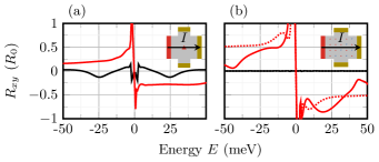
Finally, we consider the transverse resistance in a four-terminal device. The resistances of the single-antidot device and the and devices are shown in LABEL:fig:Rmeasurement.1x1 and LABEL:fig:Rmeasurement.5x4, respectively. The difference between the top and bottom chemical potentials is , and vanishes in the case of complete left-right symmetry. For spin-unpolarized electrons the system is exactly L/R symmetric and the resistance is zero (not shown). Fig. 5 shows cases with a -polarized L lead. The transverse resistances in LABEL:fig:Rmeasurement.1x1 through a single magnetic antidot (red) show clear antisymmetry with respect to energy. At positive energies, the fact that the electrons are now not flowing between L and T has the effect of shifting the potential at T closer to that at the R lead, i.e., . Simultaneously, the potential at B remains close to midway between the L and R potential, i.e., . This yields a negative transverse potential drop and in turn a negative resistance . For the spins are flipped and the sign of both the potential drop and the resistance is inverted. When the antidot is unpolarized positive and negative energies behave similarly, and the resistance is symmetric across the Fermi level, as shown in Fig. 5 (black). The same is seen for the both the array and the array devices in LABEL:fig:Rmeasurement.5x4. This clear distinction between magnetic and nonmagnetic antidots provides an excellent measure of whether the device actually splits spin currents, and can, in general, be used to detect magnetism in other nanostructured devices.
Summary. We have demonstrated that magnetic triangular antidots in graphene provide an efficient platform for spatial spin-splitting devices. The incoming current is split into output leads according to spin orientation, analogous to the spin Hall effect, but without relying on spin-orbit effects. The outgoing spin polarizations can be flipped using a gate potential. The predicted performance is robust against typical disorders present in realistic devices. The transverse resistance yields a clear signal distinguishing the magnetic nature of the perforations.
Acknowledgements.
Acknowledgments. The Center for Nanostructured Graphene (CNG) is sponsored by the Danish National Research Foundation, Project DNRF103. S.R.P. acknowledges funding from the European Union’s Horizon 2020 research and innovation programme under the Marie Skłodowska-Curie grant agreement No 665919 and the Severo Ochoa Program (MINECO, Grant No. SEV-2013-0295).References
- Castro Neto et al. (2009) A. H. Castro Neto, N. M. R. Peres, K. S. Novoselov, and A. K. Geim, Reviews of Modern Physics 81, 109 (2009).
- Han et al. (2010) W. Han, K. Pi, K. M. McCreary, Y. Li, J. J. I. Wong, A. G. Swartz, and R. K. Kawakami, Physical Review Letters 105, 167202 (2010).
- Yazyev (2010) O. V. Yazyev, Reports on Progress in Physics 73, 056501 (2010).
- Nair et al. (2012) R. R. Nair, M. Sepioni, I.-L. Tsai, O. Lehtinen, J. Keinonen, A. V. Krasheninnikov, T. Thomson, A. K. Geim, and I. V. Grigorieva, Nature Physics 8, 199 (2012).
- McCreary et al. (2012) K. M. McCreary, A. G. Swartz, W. Han, J. Fabian, and R. K. Kawakami, Physical Review Letters 109, 186604 (2012).
- Hong et al. (2012) J. Hong, E. Bekyarova, P. Liang, W. A. de Heer, R. C. Haddon, and S. Khizroev, Scientific Reports 2, 624 (2012).
- Nair et al. (2013) R. R. Nair, I.-L. Tsai, M. Sepioni, O. Lehtinen, J. Keinonen, A. V. Krasheninnikov, A. H. Castro Neto, M. I. Katsnelson, A. K. Geim, and I. V. Grigorieva, Nature Communications 4, 2010 (2013).
- Han et al. (2014) W. Han, R. K. Kawakami, M. Gmitra, and J. Fabian, Nature Nanotechnology 9, 794 (2014).
- Tuan et al. (2014) D. V. Tuan, F. Ortmann, D. Soriano, S. O. Valenzuela, and S. Roche, Nature Physics 10, 857 (2014).
- Kamalakar et al. (2015) M. V. Kamalakar, C. Groenveld, A. Dankert, and S. P. Dash, Nature Communications 6, 6766 (2015).
- Son et al. (2006) Y.-W. Son, M. L. Cohen, and S. G. Louie, Nature (London) 444, 347 (2006).
- Ozaki et al. (2010) T. Ozaki, K. Nishio, H. Weng, and H. Kino, Physical Review B 81, 075422 (2010).
- Saffarzadeh and Farghadan (2011) A. Saffarzadeh and R. Farghadan, Applied Physics Letters 98, 023106 (2011).
- Diniz et al. (2017) G. S. Diniz, E. Vernek, and F. M. Souza, Physica E: Low-dimensional Systems and Nanostructures 85, 264 (2017).
- Sheng et al. (2010) W. Sheng, Z. Y. Ning, Z. Q. Yang, and H. Guo, Nanotechnology 21, 385201 (2010).
- Zeng et al. (2010) M. G. Zeng, L. Shen, Y. Q. Cai, Z. D. Sha, and Y. Feng, Applied Physics Letters 96, 042104 (2010).
- Kane and Mele (2005) C. L. Kane and E. J. Mele, Physical Review Letters 95, 226801 (2005).
- Abanin et al. (2006) D. A. Abanin, P. A. Lee, and L. S. Levitov, Physical Review Letters 96, 176803 (2006).
- Balakrishnan et al. (2014) J. Balakrishnan, G. K. W. Koon, A. Avsar, Y. Ho, J. H. Lee, M. Jaiswal, S.-J. Baeck, J.-H. Ahn, A. Ferreira, M. A. Cazalilla, A. H. Castro Neto, and B. Özyilmaz, Nature Communications 5, 4748 (2014).
- Cresti et al. (2014) A. Cresti, D. Van Tuan, D. Soriano, A. W. Cummings, and S. Roche, Physical Review Letters 113, 246603 (2014).
- Sinova et al. (2015) J. Sinova, S. O. Valenzuela, J. Wunderlich, C. H. Back, and T. Jungwirth, Reviews of Modern Physics 87, 1213 (2015).
- Hu et al. (2014) H. Hu, Z. Wang, and F. Liu, Nanoscale Research Letters 9, 690 (2014).
- Pruneda (2010) J. M. Pruneda, Physical Review B 81, 161409 (2010).
- Yazyev and Helm (2007) O. V. Yazyev and L. Helm, Physical Review B 75, 125408 (2007).
- Palacios et al. (2008) J. J. Palacios, J. Fernández-Rossier, and L. Brey, Physical Review B 77, 195428 (2008).
- Leconte et al. (2011) N. Leconte, D. Soriano, S. Roche, P. Ordejón, J.-C. Charlier, and J. J. Palacios, ACS Nano 5, 3987 (2011).
- Wimmer et al. (2008) M. Wimmer, İ. Adagideli, S. Berber, D. Tománek, and K. Richter, Physical Review Letters 100, 177207 (2008).
- Wang et al. (2009) B. Wang, J. Wang, and H. Guo, Physical Review B 79, 165417 (2009).
- Zheng et al. (2009) X. H. Zheng, G. R. Zhang, Z. Zeng, V. M. García-Suárez, and C. J. Lambert, Physical Review B 80, 075413 (2009).
- Potasz et al. (2012) P. Potasz, A. D. Güçlü, A. Wójs, and P. Hawrylak, Physical Review B 85, 075431 (2012).
- Hong et al. (2016) X. K. Hong, Y. W. Kuang, C. Qian, Y. M. Tao, H. L. Yu, D. B. Zhang, Y. S. Liu, J. F. Feng, X. F. Yang, and X. F. Wang, The Journal of Physical Chemistry C 120, 668 (2016).
- Khan et al. (2016) M. E. Khan, P. Zhang, Y.-Y. Sun, S. B. Zhang, and Y.-H. Kim, AIP Advances 6, 035023 (2016).
- Gregersen et al. (2016) S. S. Gregersen, S. R. Power, and A.-P. Jauho, Physical Review B 93, 245429 (2016).
- Pedersen et al. (2008) T. G. Pedersen, C. Flindt, J. G. Pedersen, N. A. Mortensen, A.-P. Jauho, and K. Pedersen, Physical Review Letters 100, 136804 (2008).
- Petersen et al. (2011) R. Petersen, T. G. Pedersen, and A.-P. Jauho, ACS Nano 5, 523 (2011).
- Ouyang et al. (2011) F. Ouyang, S. Peng, Z. Liu, and Z. Liu, ACS Nano 5, 4023 (2011).
- Tao et al. (2011) C. Tao, L. Jiao, O. V. Yazyev, Y.-C. Chen, J. Feng, X. Zhang, R. B. Capaz, J. M. Tour, A. Zettl, S. G. Louie, H. Dai, and M. F. Crommie, Nature Physics 7, 616 (2011).
- Hashimoto et al. (2014) T. Hashimoto, S. Kamikawa, D. Soriano, J. G. Pedersen, S. Roche, and J. Haruyama, Applied Physics Letters 105, 183111 (2014).
- Magda et al. (2014) G. Z. Magda, X. Jin, I. Hagymási, P. Vancsó, Z. Osváth, P. Nemes-Incze, C. Hwang, L. P. Biró, and L. Tapasztó, Nature (London) 514, 608 (2014).
- Auton et al. (2016) G. Auton, R. K. Kumar, E. Hill, and A. Song, Journal of Electronic Materials (2016), 10.1007/s11664-016-4938-y.
- Shi et al. (2011) Z. Shi, R. Yang, L. Zhang, Y. Wang, D. Liu, D. Shi, E. Wang, and G. Zhang, Advanced Materials 23, 3061 (2011).
- Oberhuber et al. (2013) F. Oberhuber, S. Blien, S. Heydrich, F. Yaghobian, T. Korn, C. Schüller, C. Strunk, D. Weiss, and J. Eroms, Applied Physics Letters 103, 143111 (2013).
- Jin et al. (2009) C. Jin, F. Lin, K. Suenaga, and S. Iijima, Physical Review Letters 102, 195505 (2009).
- Gilbert et al. (2017) S. M. Gilbert, G. Dunn, T. Pham, B. Shevitski, E. Dimitrov, S. Aloni, and A. Zettl, 1, 4 (2017), arXiv:1702.01220 .
- Güçlü et al. (2010) A. D. Güçlü, P. Potasz, and P. Hawrylak, Physical Review B 82, 155445 (2010).
- Saremi (2007) S. Saremi, Physical Review B 76, 184430 (2007).
- Power and Ferreira (2013) S. Power and M. Ferreira, Crystals 3, 49 (2013).
- Lewenkopf and Mucciolo (2013) C. H. Lewenkopf and E. R. Mucciolo, Journal of Computational Electronics 12, 203 (2013).
- Bahamon et al. (2013) D. A. Bahamon, A. H. Castro Neto, and V. M. Pereira, Physical Review B 88, 235433 (2013).
- Koniakhin (2014) S. V. Koniakhin, The European Physical Journal B 87, 216 (2014).
- Power and Jauho (2014) S. R. Power and A.-P. Jauho, Physical Review B 90, 115408 (2014).
- Note (1) See Supplemental Material [appended] for magnetic and transport properties of triangular antidots when varying side length and introducing edge disorder.
Nanostructured graphene for spintronics
Supplemental Material
I Magnetic moment profiles and disorder
We consider here the moment profiles of the minimum and maximum side length triangles that can occur occur in the disordered samples in Fig 4 of the main text.
As shown in LABEL:fig:supplementmoments.L3, LABEL:fig:supplementmoments.L5, LABEL: and LABEL:fig:supplementmoments.L7 these profiles are similar regardless of side length. Extended zz-edges yield local profiles resembling those of graphene zz-nanoribbon edges, while corners display reduced profiles. With edge disorder however, see LABEL:fig:supplementmoments.L5.d where two edge atoms have been removed, the magnetic moment profile may be significantly reduced. Particularly so if segments become too short to support magnetic states (not shown). While removing the top corner atom has little influence, the edge atom on the right side reduces the local edge magnetic moments to almost zero.
II Transport versus side length
The electronic transport, governed by the magnetic profiles, also behaves similarly for different side lengths. In Fig. S2, the currents are displayed using single antidot or arrays antidots of either or . In comparison the two different sizes yield very similar spin dependent scattering. Both display the same top-bottom spatial spin-splitting seen in the main text Figs. 2 and 3 with .
The corresponding spin splitting efficiencies (introduced in the main text) are shown in Fig. S3. These are illustrated for the single antidot, the array, and the array where every second antidot has been rotated () in LABEL:fig:supplementefficiency.1x1, LABEL:fig:supplementefficiency.5x4, LABEL: and LABEL:fig:supplementefficiency.5x4r, respectively. Two main results are: (1) while arrays display enhanced efficiencies, the arrays yield the largest efficiencies, and (2) increasing side lengths also gives larger efficiencies. Furthermore, in LABEL:fig:supplementefficiency.1x1.varyL, LABEL:fig:supplementefficiency.5x4.varyL, LABEL: and LABEL:fig:supplementefficiency.5x4r.varyL the efficiencies are shown varying side length beyond what is considered in the main text. At both of the two energies (solid line, energy of the current maps) and (dashed line), increasing the side length in general increases the efficiencies.
III Disordered antidots transport
We now consider transport through devices with edge-disordered triangles. The transport properties are displayed in Fig. S4.
Even though the splitting of the current is very different in the disordered single antidot case shown in LABEL:fig:supplementdisorder.1x1.c and LABEL:fig:supplementdisorder.1x1.s, interestingly, the disordered arrays in LABEL:fig:supplementdisorder.5x4.c and LABEL:fig:supplementdisorder.5x4.s are remarkably similar to the pristine cases of in Figs. 2 and 3 of the main text, suggesting conserved spatial spin splitting. This point is further illustrated with the individual transmissions in LABEL:fig:supplementdisorder.5x4.LT, LABEL:fig:supplementdisorder.5x4.LB, LABEL: and LABEL:fig:supplementdisorder.5x4.LR. The disordered transmissions (solid) also show spin splitting over a wide range of energies, albeit often lower in magnitude compared to the pristine case of (dotted). Despite the fluctuations in individual transmissions, in LABEL:fig:supplementdisorder.5x4.eff the splitting efficiencies remain similar to the pristine case across a broad energy range.