Disorder enabled band structure engineering of a topological insulator surface
Abstract
Three dimensional topological insulators are bulk insulators with topological electronic order that gives rise to conducting light-like surface states. These surface electrons are exceptionally resistant to localization by non-magnetic disorder, and have been adopted as the basis for a wide range of proposals to achieve new quasiparticle species and device functionality. Recent studies have yielded a surprise by showing that in spite of resisting localization, topological insulator surface electrons can be reshaped by defects into distinctive resonance states. Here we use numerical simulations and scanning tunneling microscopy data to show that these resonance states have significance well beyond the localized regime usually associated with impurity bands. At native densities in the model Bi2X3 (X=Bi, Te) compounds, defect resonance states are predicted to generate a new quantum basis for an emergent electron gas that supports diffusive electrical transport.
Three dimensional topological insulators (TI) with the chemical formula M2X3 (M=Bi, Sb; X=Se, Te) are characterized by a single-Dirac-cone surface state M2X3prediction ; MatthewNatPhys ; YulinBi2Te3 , and have been widely investigated as model materials for TI surface physics. Shortly after the discovery of the first TI’s, it was established that standard effects of defect disorder such as backscattering and localization are greatly suppressed in TI surface states TIbasics1 ; TIbasics2 ; TIbasics3 ; TIbasics4 ; MooreInvariants ; magnetoelectric ; STM_protection ; STM_protection2 . Together with the intuition that topological properties of band structure should be inherently impervious to weak perturbations, this led to a pervasive characterization that topological interfaces are essentially blind to the presence of non-magnetic defects. It is only with the recent advent of more detailed non-perturbative numerical investigations and targeted scanning tunneling microscopy (STM) experiments STM_SeVacRes ; stepHistogramMBE ; Biswas_pointRes ; B_S_strongImpurities ; B_S_bulkRes ; newBasisB_S ; STMstepBoundState ; STMstepBoundState2 ; ZhangQPinterference ; topoFriedel ; BiswasStep ; GFtheory ; quantumCorrals ; Fabry_Perot that elements of this picture have been overturned. It is now known that, rather than being blind to defects, topological Dirac cone electrons actually bind loosely to atomic point defects in energy levels that fall very close to the Dirac point (see states labeled “resonance” in Fig. 1b), and can radically redefine electronic structure relevant to the Dirac transport regime.
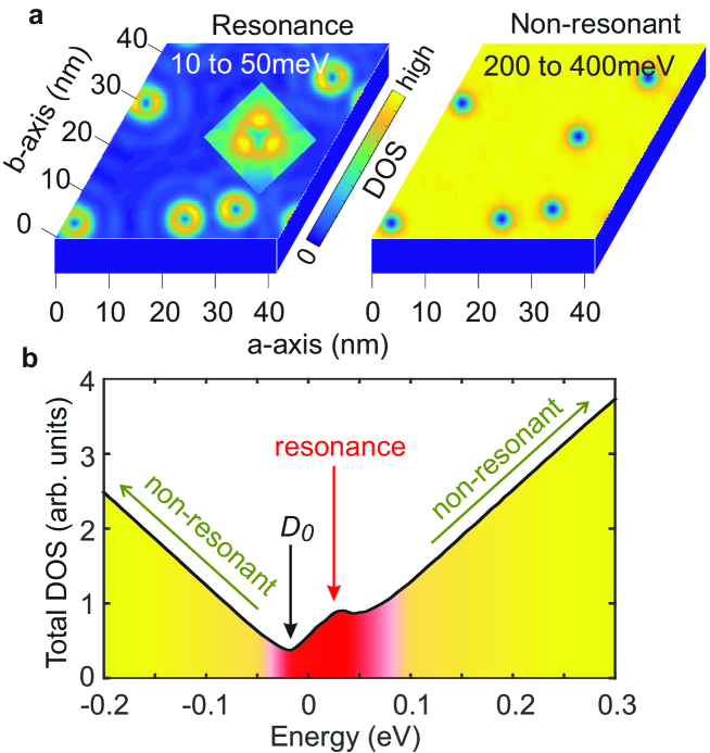
In isotropic Dirac models of TI surface states, strongly perturbing non-magnetic defects are theoretically expected to create circular s-wave resonance states, such as those plotted in Fig. 1a. Experimentally, these states have been observed in STM measurements of density of states (DOS) immediately above the Dirac point of topological insulator Bi2Se3 (see Fig. 1a (left) inset patch). Three bright spots in the STM image represent coherent interference with a slight 1 admixture of f-wave symmetry (See Supplementary Note 2) due to anisotropy not considered in the accompanying simulation. The combined impact of multiple randomly distributed defects on the electronic structure has not yet been evaluated, and is the subject of the present work.
Theoretical treatments of lattice defects are usually carried out in the single impurity approximation, since multiple impurities do not lead to emergent coherent bandstructures. Large modifications to the band structure of non-TI materials are only achieved through heterostructure growth or fractional alloying. The “impurity bands” associated with electrons on minority impurity sites are generally disregarded as being non-ideal for electronic transport. These bands exhibit miniscule dispersions, and strong defect potentials or reduced dimensionality cause the electronic states to be Anderson localized AL ; AL2D over relevant device lengthscales. A typical example is the well-studied manganese impurity band in Ga1-xMnxAs, whose dispersion across the Brillouin zone is far smaller than its intrinsic width along the energy axis, meaning that the electrons are effectively localized to isolated lattice sites MnGaAsattribution ; MnGaAsARPES .
In the following, in contrast, we find that uncompensated lattice defects at low densities () in non-amorphous TIs provide a mechanism for band structure engineering that is not shared in a conventional semiconducting system. Theoretically, it is expected that Anderson localization will be forbidden on the TI surface with non-magnetic impurities noAL1 ; noAL2 ; noAL3 ; noAL4 ; noAL5 and backscattering is suppressed relative to forward scattering STM_protection ; TIbasics1 ; TIbasics2 , leading to greater itinerancy for impurity-derived band structure. Moreover, the electronic density of states falls to zero at a surface Dirac point, making it possible for defect resonance states to dominate the absolute density of states. In the following discussions we will show that these conditions enable new defect-derived electronic dispersions, providing viable channels for diffusive electrical transport. We also find that these emergent electronic band structures can superficially appear to be gapped, and resemble Dirac point anomalies that have been seen by angle resolved photoemission spectroscopy (ARPES) in TI compounds that have no known time reversal symmetry broken ground state gapAnomalies ; hedgehog ; ChrisGMsigma ; MiaoPNAS .
I Results
I.1 Defect resonance states of Dirac electrons
We will focus on defect resonance states in the popular Bi2Se3-xTex family of single-Dirac-cone TIs M2X3prediction ; MatthewNatPhys ; YulinBi2Te3 , so as to make quantitative comparisons to STM measurements. However, our results are applicable to other TI surface states with isolated Dirac cones. In this material family, structural point defects tend to occur with a density of % per formula unit, and have been found to overlap with the surface state in the outermost quintuple layer of the lattice STM_SeVacRes ; WeidaNew (see Supplementary Note 1). Intensive characterization of Bi2Se3 has found that the density and type-range of defects can be tuned over a broad range by adjusting sample growth conditions WeidaNew . For Se-poor and stoichiometric synthesis, defects near a cleaved surface are predominantly selenium vacancies positioned in the center of the outermost quintuple layer of the lattice. Interstitial atoms and replacement defects can be common at the surface of Se-rich or quench-cooled samples. The chemical potential can be shifted as a separate parameter via methods that include bulk doping, surface dosing, and electrostatic gating DavidTunable ; JoeDiracMagnetism ; WraySCnatPhys ; WrayFe .
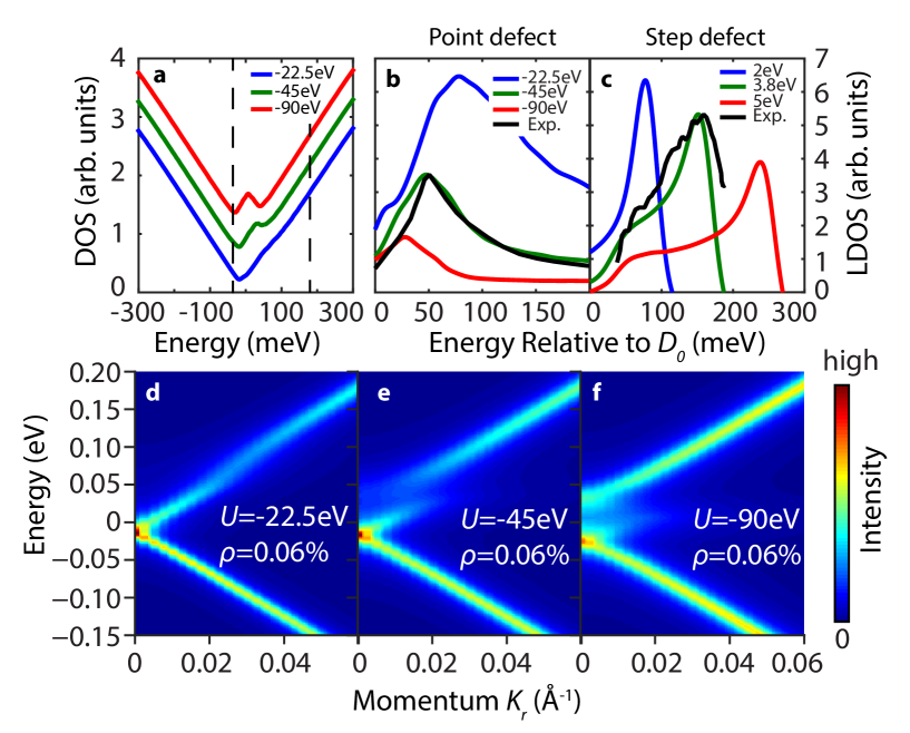
Defect resonance states have been observed by STM less than 200 meV above the surface Dirac point, surrounding point defects STM_SeVacRes ; stepHistogramMBE and at step edges between plateaus differing in height by one quintuple layer STMstepBoundState ; STMstepBoundState2 . Characteristic local density of states (LDOS) distributions measured by STM at the defect lattice sites are plotted as black curves in Fig. 2b-c. Theoretical analyses of isolated local impurities have shown that these resonance states arise naturally when strong scalar potentials are introduced to a surface occupied by spin-helical TI Dirac cone electrons STM_SeVacRes ; Biswas_pointRes ; B_S_strongImpurities ; B_S_bulkRes ; newBasisB_S . For an isolated defect described as a point potential with amplitude , the resonance state is split from the Dirac point by an energy roughly proportional to .
In the following, we numerically approach the problem of multiple impurity scattering on the surface states of TIs with a single Dirac cone, which is otherwise theoretically intractable. We use a basis of spinor plane waves Ryu2 on a discrete hexagonal real-space lattice, with lattice parameter corresponding to Bi2Se3-xTex surface atomic spacings. We have used the impurity-free spin-helical Hamiltonian, , with Dirac velocity =3.0 eV chosen to be intermediate between Bi2Se3 and Bi2Te3.
When a large surface with a typical defect density is modeled in this way, we find that approximately 2 electronic states per defect are added near the Dirac point (see Supplementary Note 1 and Supplementary Fig. 4), resulting in a new DOS peak that becomes increasingly visible as the defect potential grows (Fig. 2a). Isolating the LDOS at defect cores on Bi2Se3 reveals that a defect potential of eV accurately reproduces the resonance state energy and LDOS line shape obtained in STM studies, which is plotted in Fig. 2b. The very different experimental line shape of a step edge defect can likewise be reproduced by considering the tunneling barrier generated with a repulsive potential of eV applied to each atom along the step edge path (Fig. 2c). These comparisons are evidence that our numerical approach is able to quantitatively capture the physics observed in experiments.
I.2 New delocalized electronic structure
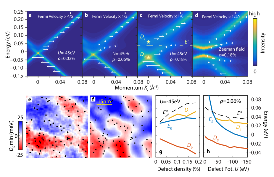
The resonance states associated with this defect distribution reveal a novel structure in the momentum-resolved electron annihilation (ARPES) spectral function, modeled in Fig. 2d-f. The resonance itself shows up as a discontinuity in the ARPES spectral function. As the defect potential strength increases, the surface Dirac point (termed ) as well as the discontinuity associated with the resonance state LDOS maximum () move down in energy (Fig. 3h). When the defect potential crosses a critical value of eV, a new local maximum appears in the spectrum at ( point), roughly meV above the Dirac point, and will henceforth be referred to as ‘’. As the defect resonance state converges on eV with increasing potential strength, the region between and begins to qualitatively resemble a band gap, as has been seen at the Dirac point of TI crystals with non-magnetic defects in Ref. gapAnomalies ; hedgehog . Unlike a true band gap, which is theoretically disallowed TIbasics3 , the momentum-integrated total DOS distribution contains a local maximum within the seemingly gapped region (Fig. 2a).
A remarkable evolution of the electronic structure also occurs when the defect density is increased (see Fig. 3a-c series). When the defect density is tripled to , the faint local maximum becomes the dispersion minimum of an upper band that is clearly disconnected from the Dirac cone. The upper Dirac cone maintains its dispersion for small momenta , out to more than 50meV from the Dirac point, and becomes dispersionless at larger momenta, as would be expected for a more typical impurity band. For all of these impurity densities, the upper Dirac cone dispersion is significantly larger than the energy axis intrinsic width, which is and 0.04 eV at half maximum intensity in Fig. 3b-c, respectively.
Higher defect densities are also associated with further lowering of the Dirac point energy. An STM map obtained on a Se vacancy-rich Bi2Se3-δ surface shows that spatial fluctuations in the energy of the LDOS minimum are highly correlated with defect density (see Fig. 3e). Simulating the observed Se vacancies with a defect potential reproduces the qualitative spatial distribution of the LDOS minimum (Fig. 3f). These modeling results can be plotted in the same 25 meV range as the STM data, showing that the energy scale of fluctuations is accurately captured, even though fine details may be inconsistent due to missing information about defects outside of the STM map, or deeper in the crystal. We note that the spatial distribution of defects observed by STM is very uniform and uncorrelated, and is not readily distinguished from the random defect configurations used in our simulations (see Poisson distribution overlay in Supplementary Fig. 1).
The emergence of new spectral features at high defect density is closely related to the fraction of states near the Dirac point that can be attributed as defect resonance states. In the absence of defects, the total number of states within an energy of the Dirac point is , where is the total number of 2D surface lattice sites. Setting equal to the approximate number of resonance states () gives a new energy scale, , which we find to have a novel physical significance. As can be see in Fig. 3g-h, we find that a local maximum associated with the emergent feature becomes visible when the resonance state energy becomes smaller than . These simulations also reveal that the resonance energy may be tuned not only by changing the impurity strength, as has been theoretically predicted before, but also by increasing the impurity concentration, a fact that is technologically significant because the impurity strength is usually not tunable. With the experimentally fitted defect potential eV, the resonance energy crosses when the defect density becomes larger than , resulting in the easily visible emergent features in Fig. 3b-c.
To evaluate the ability of the emergent coherent impurity band-like features to carry mobile charge, we have calculated the twist velocity, , for configurations with sites (300 sites = 126nm/side). These are shown in Figs. 3a-c as vectors overlaid at local maxima of the modeled ARPES spectrum. The twist velocity of a quantum state is proportional to the magnitude of a persistent DC current carried by that state in the presence of an electric field (see Methods), and in the scattering-free limit is equivalent to the group velocity of the electronic band. It is calculated as the gradient of the state energies with respect to a phase twist around the system boundary.
We find that the twist velocities of band features at energies eV have similar amplitudes, and are approximately proportional to the apparent slope in momentum space, suggesting that all of these features are viable bands for charge transport. However, twist velocities decay towards zero as the upper Dirac cone disperses into the seemingly gapped region beneath the feature, particularly at momenta of , and this may greatly limit carrier mobility for certain values of the chemical potential (see evaluation of twist and band velocities in Supplementary Note 1, Supplementary Fig. 2 and Supplementary Fig. 3). Velocities are relatively large in the lower Dirac cone, where states are energetically distant from the resonance states, and maximal velocities are found immediately beneath , where elastic scattering is minimal due to the vanishing density of states near a 2D Dirac point.
For comparison, a similar simulation with magnetic defects instead of a eV scalar field is shown in Fig. 3d, representing a case in which the topological protection against Anderson localization is expected to fail Rudro_magneticDopants . We have approximated each magnetic defect by a localized eV exchange field perfectly aligned with the +z-axis, perpendicular to the surface (see Methods). In this magnetic scenario, even though disorder of the magnetic moment vectors has been neglected, twist velocities are still reduced by an additional order of magnitude near the Dirac point due to Anderson localization.
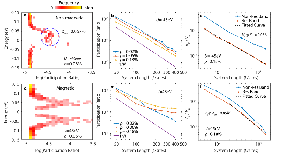
We have also investigated the transport characteristics of the potential disorder-induced band structure by an alternate metric, the participation ratios of the quantum eigenstates. The participation ratio PR1 ; PR2 of an electronic wavefunction is the sum of squares of the site-resolved probability densities (see Methods). For itinerant electronic states that can participate in electronic transport, it decays as the inverse of the total number of sites in the system (), for large system sizes. On the other hand, for localized states, the participation ratio converges on a non-zero value as system size increases beyond the localization length of the wavefunction. The participation ratios of the energy eigenstates in the presence of scalar and magnetic disorder are compared in Fig. 4. We find that in the latter case, Anderson localized states around the resonances display large participation ratios that saturate with system size (Fig. 4e), while topological protection against localization ensures that the participation ratios for the comparable scalar potential disorder case vary inversely as the system size, for large system sizes (Fig. 4b). Calculating the twist velocities for larger system sizes shows a similar trend (Fig. 4c,f), in which scalar defect potentials allow diffusive transport (), being topologically protected against Anderson localization, unlike conventional impurity bands, represented here by the same surface states in the presence of magnetic disorder of comparable strength.
II Discussion
Impurity-induced carrier control is the cornerstone of the semiconductor industry, and band structure engineering via disorder is the natural successor of such disorder-induced functionalization of electronic materials. In conventional 2D materials, Anderson localization prevents impurity bands from acting as viable carriers for diffusive charge transport. In this work, we have shown that this restriction is ameliorated in the surface states of topological insulators, in the presence of moderate potential disorder that does not break time reversal symmetry. Using numerical techniques verified by comparison to experimental observations, we have demonstrated that a new impurity band structure emerges in the TI surface states in the presence of scalar potential disorder, and that these states remain diffusive and are able to participate in transport processes. We have contrasted this novel behavior, when topological protection against localization is present, to the more conventional situation when magnetic disorder of comparable strength is present, when Anderson localization prevents diffusive transport in the impurity band.
Our results also shed light on some less understood DOS anomalies on TI surface states that have been reported in the literature. ARPES experiments have previously resolved gap-like features gapAnomalies ; hedgehog ; ChrisGMsigma and Dirac point elongation MiaoPNAS in the spectrum of TI surface states, in the absence of any time-reversal breaking effects. The experiment in Ref. ChrisGMsigma presents a particularly telling case. In this work, incident photon polarization was tuned to eliminate the dominant even-symmetry photoemission channel from Bi2Se3 along the high symmetry axis. Defect resonance states do not have spatial reflection symmetry due to their random distribution, and would not be intrinsically suppressed by this symmetry factor. This defect-sensitive measurement geometry revealed a gap-like dispersion, with the upper Dirac cone bands appearing to converge more than meV above the Dirac point, as expected from our calculations for the feature.
We have shown that these observations may be attributed to the effects discussed above, arising from scalar potential disorder alone. The emergent band structure associated with defects is very narrowly separated from nearby bands in momentum, and will be difficult to cleanly resolve in ARPES experiments. The energy-axis widths of bands in our calculations are 2-3 times narrower than those actually observed in Bi2Se3, indicating that factors not considered here such as phonon scattering and surface inhomogeneity may play a significant role in the low energy physics, and may obscure the role of defect-derived states.
Nonetheless, the existence of defect resonance states immediately above the Dirac point of these compounds is well known from STM measurements, and the new physics discussed in this work are direct consequences of the interplay between these resonance states and other established elements of TI surface physics. The numerical evaluations of electron mobility and localization discussed above show that the emergent band structure identified in these simulations is viable as a basis for conductivity, and that band structure engineering is possible via non-magnetic defects in a TI system, driven by unique factors such as the lack of Anderson localization and the vanishing of DOS near a 2D Dirac point.
III Methods
III.1 Energetics and state basis at the TI surface
STM data and LDOS curves were obtained by the procedures described in Ref. STM_SeVacRes ; STMstepBoundState . The surface state is modeled as a spin-helical 2D Dirac cone occupying a discrete hexagonal real-space lattice with repeating boundary conditions, and is essentially a discretized version of the model in Ref. Biswas_pointRes ; STM_SeVacRes . The kinetic Hamiltonian is given by , with velocity =3.0 eV chosen to be intermediate between Bi2Se3 and Bi2Te3. The real space basis includes two spin-degenerate states per lattice site. The kinetic Hamiltonian is diagonalized on this basis, and the resulting momentum-space basis is reduced by applying a high energy cutoff W=0.4 eV to exclude high energy states that would not conform to a Dirac dispersion.
Defects are created by perturbing sites at selected coordinates with a scalar energy term. as , where is the number operator, and the full Hamiltonian is diagonalized. The convention of creating point defects as triangular 3-site clusters with a perturbation strength of on each site is adopted to give 3-fold rotational symmetry as seen experimentally STM_SeVacRes ; stepHistogramMBE , though calculated spectra do not strongly differentiate between differently sized small site clusters (see Supplementary Fig. 6). The Hamiltonian is numerically diagonalized, and the ARPES spectral function is defined as the energy- and momentum-resolved spectral function of single particle annihilation, convoluted by a 10 meV half-width Lorentzian:
| (1) |
This represents the spectral function for photoemission with z-axis photon polarization, which acts with even reflection symmetry and removes electrons from the dominant orbital component of the Bi2Se3-xTex surface state. Energy-momentum dispersions were found to be rotationally isotropic, and have been rotationally averaged to obtain a small spacing between states on the momentum axis. Figures in the paper use the rotationally averaged ‘radial’ momentum (), and single-axis spectral functions can be found in Supplementary Fig. 5. For smaller system sizes considered in Fig. 4, it was necessary to average over several randomly generated defect configurations to achieve convergence of the twist velocity and participation ratio. Additional modeling details are found in Supplementary Note 3.
III.2 Metrics of localization
Adding a phase twist at the system boundary provides an easy way to identify the degree to which electronic states are localized. This is achieved by the standard method of shifting the momentum (K-space) basis of the Hilbert space by an offset of , where () is the width of the system along the x- (y-) axis. A velocity termed the “twist velocity” can be calculated for individual eigenstates as (using numerical derivatives), and represents the velocity of a persistent current. The energy- and momentum-resolved twist velocity () displayed on ARPES spectral intensity maxima in Fig. 3 is calculated via a weighted average of states within of the energy E, as:
| (2) |
Here, represents the free particle eigenstates that have momentum . When divided by the width of the system L along the indicated axis, the momentum twist has units of wave number. The numerical derivative is performed at a small but nonzero twist value of along the direction to break degeneracies and avoid possible finite size nesting effects.
The participation ratio is defined as:
| (3) |
where the sum is over all sites in the system, and is the LDOS on site of , which is an eigenstate of the full Hamiltonian.
III.3 Data availability
The data and source code that support the findings of this study are available from the corresponding authors on reasonable request.
Acknowledgements: We are grateful for discussions with W. Wu, P. Hohenberg and Y.-D. Chuang. Work at Stanford University was supported by the Department of Energy Grant DE-AC02-76SF00515. R.R.B. was supported by Purdue University startup funds.
Authors Contribution: Y.X. and J.C. carried out the numerical modeling with assistance from H.H. and guidance from R.R.B. and L.A.W.; Y.X., J.C., L.M., R.R.B. and L.A.W. participated in the analysis, figure planning and draft preparation; Z.A. and A.K. performed and analyzed the STM experiments; L.A.W. was responsible for the conception and the overall direction, planning and integration among different research units.
Competing interests: The authors declare no competing financial interests.
References
- (1) [
- (2) Zhang, H. et al. Topological insulators in Bi2Se3, Bi2Te3 and Sb2Te3 with a single Dirac cone on the surface. Nat. Phys. 5, 438-442 (2009).
- (3) Xia, Y. et al. Observation of a large-gap topological-insulator class with a single Dirac cone on the surface. Nat. Phys. 5, 398-402 (2009).
- (4) Chen Y. L. et al. Experimental Realization of a Three-Dimensional Topological Insulator, Bi2Te3. Science 325, 178-181 (2009).
- (5) Hasan, M. Z. & Kane, C. L. Colloquium: Topological insulators. Rev. Mod. Phys. 82, 3045 (2010).
- (6) Qi, X.-L. & Zhang, S.-C. Topological insulators and superconductors. Rev. Mod. Phys. 83, 1057 (2011).
- (7) Fu, L., Kane, C. L. & Mele, E. J. Topological Insulators in Three Dimensions. Phys. Rev. Lett. 98, 106803 (2007).
- (8) Hsieh, D. et al., Observation of Unconventional Quantum Spin Textures in Topological Insulators. Science 323, 919-922 (2009).
- (9) Moore, J. E. & Balents, L. Topological invariants of time-reversal-invariant band structures. Phys. Rev. B 75, 121306 (2007).
- (10) Roushan, P. et al. Topological surface states protected from backscattering by chiral spin texture. Nature 460, 1106-1109 (2009).
- (11) Alpichshev, Z. et al. STM Imaging of Electronic Waves on the Surface of Bi2Te3: Topologically Protected Surface States and Hexagonal Warping Effects. Phys. Rev. Lett. 104, 016401 (2010).
- (12) Qi, X.-L., Hughes, T. L. & Zhang, S.-C. Topological field theory of time-reversal invariant insulators. Phys. Rev. B 78, 195424 (2008).
- (13) Black-Schaffer, A. M. & Yudin, D. Spontaneous gap generation on the surface of weakly interacting topological insulators using nonmagnetic impurities. Phys. Rev. B 90, 161413(R) (2014).
- (14) Biswas, R. R. & Balatsky, A. V. Impurity-induced states on the surface of three-dimensional topological insulators. Phys. Rev. B 81, 233405 (2010).
- (15) Teague, M. L. et al. Observation of Fermi-energy dependent unitary impurity resonances in a strong topological insulator Bi2Se3 with scanning tunneling spectroscopy. Solid State Comm. 152, 747-751 (2012).
- (16) Alpichshev, Z. et al. STM Imaging of Impurity Resonances on Bi2Se3. Phys. Rev. Lett. 108, 206402 (2012).
- (17) Black-Schaffer, A. M. & Balatsky, A. V. Subsurface impurities and vacancies in a three-dimensional topological insulator. Phys. Rev. B 86, 115433 (2012).
- (18) Black-Schaffer, A. M. & Balatsky, A. V. Strong potential impurities on the surface of a topological insulator. Phys. Rev. B 85, 121103(R) (2012).
- (19) Alpichshev, Z., Analytis, J. G., Chu, J.-H., Fisher, I. R. & Kapitulnik, A. STM imaging of a bound state along a step on the surface of the topological insulator Bi2Te3. Phys. Rev. B 84, 041104(R) (2011).
- (20) Dmitriev, A. Yu., Fedotov, N. I., Nasretdinova, V. F. & Zaitsev-Zotov, S. V., Effect of surface defects and few-atomic steps on the local density of states of the atomically-clean surface of Bi2Se3 topological insulator. JETP Letters, 100, 398-402 (2014).
- (21) Wang, J. et al., Power-law decay of standing waves on the surface of topological insulators. Phys. Rev. B 84, 235447 (2011).
- (22) Biswas, R. R. & Balatsky, A. V., Scattering from surface step edges in strong topological insulators. Phys. Rev. B 83, 075439 (2011).
- (23) Rizzo, B., Arrachea, L. & Moskalets, M. Transport phenomena in helical edge state interferometers: A Green’s function approach. Phys. Rev. B 88, 155433 (2013).
- (24) Fu, Z. G., Zhang, P., Wang, Z. & Li, S. S. Quantum corrals and quantum mirages on the surface of a topological insulator. Phys. Rev. B 84, 235438 (2011).
- (25) Fu, Z. G. et al. Anisotropic Fabry-P rot resonant states confined within nano-steps on the topological insulator surface. Sci Rep. 4, 5544 (2014).
- (26) Liu, Q., Qi, X.-L. & Zhang, S.-C. Stationary phase approximation approach to the quasiparticle interference on the surface of a strong topological insulator. Phys. Rev. B 85, 125314 (2012).
- (27) Anderson, P. W., Absence of Diffusion in Certain Random Lattices. Phys. Rev. 109, 1492-1505 (1958).
- (28) Abrahams, E., Anderson, P. W., Licciardello, D. C. & Ramakrishnan, T. V., Scaling Theory of Localization: Absence of Quantum Diffusion in Two Dimensions. Phys. Rev. Lett. 42, 673-676 (1979).
- (29) Ernst, A., Sandratskii, L. M., Bouhassoune, M., Henk, J. & Lüders, M. Weakly Dispersive Band near the Fermi Level of GaMnAs Due to Mn Interstitials. Phys. Rev. Lett. 95, 237207 (2005)
- (30) Okabayashi, J. et al., Angle-resolved photoemission study of Ga1-xMnxAs. Phys. Rev. B 64, 125304 (2001).
- (31) Konig, E. J., Ostrovsky, P. M., Protopopov, I. V., & Mirlin, A. D. Metal-insulator transition in two-dimensional random fermion systems of chiral symmetry classes. Phys. Rev. B 85, 195130 (2012).
- (32) Fu, L. & Kane, C. L. Topology, Delocalization via Average Symmetry and the Symplectic Anderson Transition. Phys. Rev. Lett. 109, 246605 (2012).
- (33) Ostrovsky, P. M., Gornyi, I. V. & Mirlin, A. D. Interaction-Induced Criticality in Z2 Topological Insulators. Phys. Rev. Lett. 105, 036803 (2010).
- (34) Ostrovsky, P. M., Gornyi, I. V. & Mirlin, A. D. Quantum Criticality and Minimal Conductivity in Graphene with Long-Range Disorder. Phys. Rev. Lett. 98, 256801 (2007).
- (35) Ryu, S., Mudry, C., Obuse, H. & Furusaki, A. Z2 Topological Term, the Global Anomaly, and the Two-Dimensional Symplectic Symmetry Class of Anderson Localization. Phys. Rev. Lett. 99, 116601 (2007).
- (36) Xu, S.-Y. et al. Hedgehog spin texture and Berry’s phase tuning in a magnetic topological insulator. Nat. Phys. 8, 616-622 (2012).
- (37) Xu, S.-Y. et al. Dirac point spectral weight suppression and surface ”gaps” in nonmagnetic and magnetic topological insulators. Preprint at “http://arxiv.org/abs/1206.0278v3” (2012).
- (38) Jozwiak, C. et al. Photoelectron spin-flipping and texture manipulation in a topological insulator. Nat. Phys. 9, 293-298 (2013).
- (39) Miao, L. et al. Quasiparticle dynamics in reshaped helical Dirac cone of topological insulators. Proc. Nat. Acad. Sci. 110, 2758-2762 (2013).
- (40) Dai, J.-X. et al. Toward the Intrinsic Limit of the Topological Insulator Bi2Se3, Phys. Rev. Lett. 117, 106401 (2016).
- (41) Hsieh, D. et al., A tunable topological insulator in the spin helical Dirac transport regime. Nature 460, 1101-1105 (2009).
- (42) Checkelsky, J. G., Ye, J., Onose, Y., Iwasa, Y., & Tokura, Y. Dirac-fermion-mediated ferromagnetism in a topological insulator. Nat. Phys. 8, 729-733 (2012).
- (43) Wray, L. A. et al. Observation of topological order in a superconducting doped topological insulator. Nat. Phys. 6, 855859 (2010).
- (44) Wray, L. A. et al., A topological insulator surface under strong Coulomb, magnetic and disorder perturbations. Nature Physics 7, 32-37 (2011).
- (45) Nomura, K., Koshino, M. & and Ryu, S. Topological Delocalization of Two-Dimensional Massless Dirac Fermions. Phys. Rev. Lett. 99, 146806 (2007).
- (46) Sessi, P. et al. Dual nature of magnetic dopants and competing trends in topological insulators. Nature Communications 7, 12027 (2016).
- (47) Bell, R. J. & Dean, P. Atomic vibrations in vitreous silica. Disc. Faraday Soc. 50 55-61 (1970).
- (48) Thouless, D. J. Electrons in disordered systems and the theory of localization. Phys. Rep. 13C, 93-142 (1974).