Characterization of Traps at Nitrided SiO2/SiC Interfaces near the Conduction Band Edge by using Hall Effect Measurements
Abstract
The effects of nitridation on the density of traps at SiO2/SiC interfaces near the conduction band edge were qualitatively examined by a simple, newly developed characterization method that utilizes Hall effect measurements and split capacitance-voltage measurements. The results showed a significant reduction in the density of interface traps near the conduction band edge by nitridation, as well as the high density of interface traps that was not eliminated by nitridation.
In recent years, silicon carbide (SiC) metal-oxide semiconductor field-effect transistors (MOSFETs) have been commercialized as the next-generation, high-voltage, low-loss power devices baliga . However, even in the case of state-of-the-art SiC MOSFETs, a high MOS channel resistance caused by low mobility in the SiO2/SiC interfaces still limits their potential performance. Therefore, the improvement of mobility in SiO2/SiC interfaces remains a critical issue in the research and development of SiC MOSFETs. It was presumed that the high density of traps at the SiO2/SiC interfaces near the conduction band edge () was the cause of degradation in mobility afanasiev_pss ; saks2000 . It is therefore highly essential to acquire the fundamental knowledge on the density of traps at the interface () near , which will provide us with clues to further our understanding as to what the interface traps are and how to reduce them. However, it has been difficult to quantitatively examine the effect of on the mobility of the fabricated SiC MOSFETs. This is partly because a well-known Hi-Lo capacitance-voltage (-) method is not suitable for the characterization of the energy distribution of the density of traps at the interface () near yoshioka_psi , and partly because of the lack of knowledge of the energy range of , which directly affects the mobility of SiC MOSFETs. In fact, characterized by a Hi-Lo - method does not always correlate with the mobility Suzukiwet ; Suzukino . Unfortunately, a Hi-Lo - method is still commonly used for the screening of newly developed processes, for the improvement of a SiO2/SiC interfacerfacemos ; bariummos .
On the other hand, to expand the limit of the energy range of towards , many characterization techniques were investigated, such as deep-level transient spectroscopy, a conductance method, and so on pensl2008 ; yoshioka_psi ; hatakeyamadlts . However, it turned out that these techniques expand the characterizable energy range of to some extent, but they are not effective enough to characterize near . Consequently, we formulated a new simple and practical characterization method for near , by using a split - method and Hall effect measurements. In this letter, we first derive the formulae for this characterization method. Subsequently, this characterization method is applied to determine the effect of nitridation on near . It should be noted that the nitridation is the mainstream of the passivation process of traps at the SiO2/SiC interface Rozen .
The core idea of the new characterization method of near is to focus on the quantitative characterization of the densities of free (mobile) and trapped carriers at SiO2/SiC interfaces arnold2001 ; saks_dit ; ortiz2015 ; takagi2014 ; tsujimura ; hatakeyama2015 ; shiomimob . The physics governing the trapping of electrons at the interface is included in these two characterized quantities. However, to extract the quantitative information on from them, a careful examination of the relationship between the applied gate voltage () and the energy of the traps at the interface () is required hatakeyama2015 ; takagissdm . In the new characterization method, the errors in the relationship between the and the are minimized by the use of the analytic formulae derived from the exact solution of the Poisson equation in a MOS structure nicollian_ns .
Now, the new characterization method of near is described step by step. In the first step, the free carrier density () is characterized as a function of , by the use of Hall effect measurements for a SiC MOSFET. In the second step, the capacitance between the gate and the channel () of a SiC MOSFET is characterized as a function of a , by the use of a split - technique. In the third step, the total density of carriers at the interface, induced by the applied (), is obtained by integrating the over the scanned voltages () as follows:
| (1) |
where is the minimum value of the scanned gate voltage, which is set to be less than the threshold voltage. Finally, the trapped carrier density ( is obtained by subtracting from , as follows:
| (2) |
From these obtained functions ( and ), near is calculated according to the following formulae.
The density of the trapped electrons () as a function of the Fermi level at the interface () is given by the product of the density of interface traps and the Fermi–Dirac distribution function, as follows:
| (3) |
where and are the thermodynamic beta factor and the degeneracy factor. In this study, is assumed to be 2. When we examine and at the interface, the origin of the energy is implicitly set to the intrinsic Fermi energy of the SiC at the interface. In this notation, the changes as changes. In the standard energy diagram of a MOS interface, is essentially the same as the surface potential at the interface , as follows:
| (4) |
The derivative of Eq. 3 gives the following relationship by approximating the derivative of the Fermi–Dirac distribution function to the Dirac delta function, as follows:
| (5) |
where the shift in energy in the argument of comes from the degeneracy factor . Thus, is given by the derivative of with respect to the . The relationship between the trap energy () (which is the argument of ) and , is given by the following formula:
| (6) |
It should be noted that the measured trapped carrier density is obtained as a function of , and not . Thereby, a parametric differentiation is introduced as follows:
| (7) |
The numerator of this equation was obtained by the numerical derivative of .
| name | NO POA (min.) | (cm-3) |
|---|---|---|
| Dry | 0 | |
| NO10 | 10 | |
| NO60 | 60 | |
| NO120 | 120 |
The denominator of the equation was calculated by using , as described below. Under Fermi-Dirac statistics, the in strong inversion is approximated by a function of the , as follows nicollian_ns :
| (8) |
where , , , , , , and are the relative permittivity of SiC, vacuum permittivity, Boltzmann constant, temperature, effective density of states in the conduction band, acceptor density in the p-well, and band bending at the interface, respectively. is the energy at the bottom of the conduction band at the interface. is a complete Fermi-Dirac integral for an index of . The is the areal acceptor density in the depletion layer in a strong inversion state of a SiC MOSFET, which is approximated by the following equation:
| (9) |
where is the bulk potential. The as a function of is derived from Eq. 8 as follows:
| (10) |
where is an inverse function of . The differential equation of with respect to can be obtained by the parametric differentiation as follows:
| (11) |
where the differential of with respect to in the right hand side of the equation can be obtained by the numerical differentiation of the measured value.
In the evaluation of Eq. 10 and Eq. 11, analytical approximations of are used blackmore_fd .
The characterization method described above was applied to determine the effect of nitridation on , in SiO2/SiC interfaces.
Four types of SiC MOSFETs on Si-faces (4H-SiC (0001)) were prepared and characterized. The thickness of the thermally grown gate oxide was around 50 nm. Post-oxidation annealing in nitric oxide (NO POA) at was applied to three of the four samples. The abbreviated names, process conditions of NO POA, and doping densities of the p-well of SiC MOSFETs, are summarized in table 1. The gate electrode was phosphorus doped poly-silicon.
The Hall effect measurements, using the van der Pauw technique, were carried out to obtain and the Hall mobility () of the prepared SiC MOSFETs. The strength of the applied magnetic field is about 0.5 T. The Hall factor () is assumed to be 1.
The total carrier density () was calculated by integrating the , which was obtained by using the split-- technique with respect to the gate voltage, according to Eq. 1. The split-- measurements were conducted at 10 Hz, using the ultra-low frequency - measurement system created by Agilent Technologies. In the measurements, the gate voltage was scanned from the inversion region to the depletion region, in order to suppress the variation of the measurements caused by the shift of the threshold voltage. We note that one of the advantages of using the split - technique is that we can exclude the errors derived from the assumption of the threshold voltage, when calculating . The trapped carrier density () was obtained according to Eq. 2.
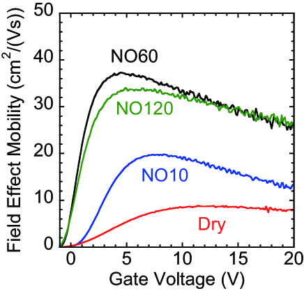
The field effect mobilities (’s) of four types of prepared SiC MOSFETs are shown in Fig. 1. It can be seen that was improved by NO POA for at least 60 min. However, the effect of nitridation on was saturated when the duration time of NO POA was more than 60 min. Furthermore, it should be noted that the observed maximum value of the of the best sample of “NO 60” is less than 40 cm(Vs). This value is much smaller than the bulk mobility of 4H-SiC, which is around 1000 cm(Vs) hatakeyamamob . By the examination of the ’s, the issues concerning the electron transport of the nitrided SiO2/SiC interfaces are summarized as follows: (1) the mechanism of improvement and the saturation of by nitridation, (2) the reason why of the nitrided SiO2/SiC interfaces is much smaller than the bulk mobility of 4H-SiC. Hereafter, we discuss these issues based on the results obtained using our new characterization method.
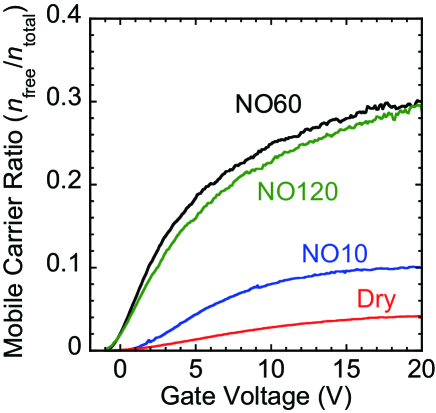
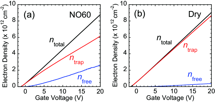
In Fig. 2 (a) and (b), the obtained , and of the “NO60” and “Dry” samples are shown. In both cases, the trapping of electrons at the interface traps is dominant. Only a portion of the electrons induced by the gate voltage contribute to the transport in SiC MOSFETs, even in the case of the “NO60” sample. To quantitatively examine the effect of trapping on the electron transport, the ratios of to (free carrier ratios) of the four prepared samples are shown in Fig. 3. As shown in Fig. 3, the free carrier ratios increased as the gate voltage was increased. The maximums of the free carrier ratios of “Dry,” “NO10,” “NO60,” and “NO120,” were 4%, 10%, 30%, and 30%, respectively. The free carrier ratio increased as the duration time of NO POA was increased up to 60 min. This relationship between the free carrier ratio and the duration time of NO POA is the same as that of the field effect mobility. Furthermore, the small free carrier ratio also explains, at least to some extent, the reason why the mobility of the nitrided SiO2/SiC interfaces is much smaller than the bulk mobility of 4H-SiC.
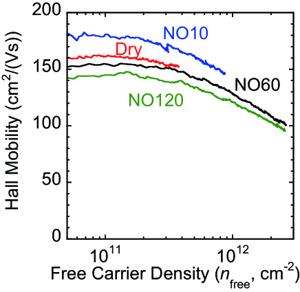
To examine the effect of nitridation on the mobility of free carriers, the ’s of the prepared samples are shown in Fig. 4 as a function of . All the ’s gradually decreased as the free carrier densities increased. A distinct correlation between the and the duration time of NO POA was not observed, whereas a weak correlation between the and the doping density of the p-well of the SiC MOSFET was observed. From Figs. 3 and 4, we conclude that the increase of the by nitridation is caused by the increase of the free carrier ratio, and not by the increase of the mobility. Furthermore, from the results obtained from Fig. 4, we can see that the was not sensitive to the reduction of caused by nitridation. We note that the trapped carriers at the interface become the Coulomb scattering centers in electron transport. Accordingly, the obtained results show that the density of the Coulomb scattering centers at the interface have a limited effect on the . Therefore, we infer that the dominant scattering mechanism of the is not the remote Coulomb scattering from the trapped carriers.
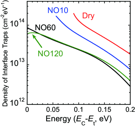
Finally, in Fig. 5, we show the ’s near , which were calculated from the measured ’s and ’s of four samples, according to the new characterization method. In Fig. 5, all the ’s are more than 1013 cm-2eV-1 around . We note that the possible errors derived from the non-unity value of the Hall factor are negligible in this casetakagissdm . Compared to the of the“Dry” sample, the ’s of the nitrided samples, are reduced down to 25 % at (eV), particularly those of “NO60” and “NO120.” However, they are still more than cm-2eV-1 around . This non-reduced near leads to the relatively low ’s of the fully nitrided “NO60” and “NO120” samples, which are shown in Fig. 1. From these results, we conclude that nitridation reduces near , but is unable to completely eliminate them.
In summary, a simple, practical, and quantitative characterization method for near was formulated by utilizing the split - technique and Hall effect measurements. This characterization method was applied to the nitrided SiO2/SiC (0001) interfaces to determine the effects of nitridation on and electron transport at the interfaces. It is concluded that nitridation reduces near , but cannot eliminate them completely. It is also concluded that is not sensitive to the change of caused by nitridation. It is inferred that the effect of Coulomb scattering from the trapped electrons on the may be limited.
Acknowledgements.
This work was supported by the Council for Science, Technology and Innovation (CSTI), Cross-ministerial Strategic Innovation Promotion Program (SIP), “Next-generation power electronics” (funding agency: NEDO).References
- (1) B. J. Baliga: Silicon Carbide Power Devices (World Scientific, Singapore, 2005).
- (2) V. V. Afanas’ev, M. Bassler, G. Pensl and M. Schulz: Phys. Status Solidi (a) 162 (1997) 321.
- (3) N. F. Saks and A. K. Agarwal: Appl. Phys. Lett. 77 (2000) 3281.
- (4) H. Yoshioka, T. Nakamura and T. Kimoto: J. Appl. Phys. 111 (2012) 014502.
- (5) T. Suzuki, J. Senzaki, T. Hatakeyama, K. Fukuda, T. Shinohe and K. Arai: Mat. Sci. Forum 600–603 (2009) 791.
- (6) T. Suzuki, J. Senzaki, T. Hatakeyama, K. Fukuda, T. Shinohe and K. Arai: Mat. Sci. Forum 615–617 (2009) 557.
- (7) T. Hiyoshi, T. Masuda, K. Wada, S. Harada and Y. Namikawa: Mat. Sci. Forum 740–742 (2013) 506.
- (8) D. J. Lichtenwalner, L. Cheng, S. Dhar, A. Agarwal and J. W. Palmour: Appl. Phys. Lett. 105 (2014) 182107.
- (9) G. Pensl, S. Beljakowa, T. Frank, K. Gao, F. Speck, T. Seyller, L. Ley, F. Ciobanu, V.Afanas’ev, A. Stesmans, T. Kimoto, A. Schöner: phys. stat. sol. (b) 245 (2008) 1378.
- (10) T. Hatakeyama, M. Sometani, K. Fukuda, H. Okumura and T. Kimoto: Jpn. J. Appl. Phys 54 (2015) 111301.
- (11) J. Rozen, S. Dhar, M. E. Zvanut, J. R. Williams and L. C. Feldman: J. Appl. Phys. 105 (2009) 124506.
- (12) E. Arnold and D. Alok: IEEE Trans. Elec. Dev. 48 (2001) 1970.
- (13) N. Saks: Silicon Carbide: Recent Major Advances, eds. W. J. Choyke, H. Matsunami and G. Pensl (Springer, 2003) p. 387.
- (14) G. Ortiz, C. Strenger, V. Uhnevionak, A. Burenkov, A. J. Bauer, P. Pichler, F. Cristiano, E. Bedel-Pereira and V. Mortet: Appl. Phys. Lett. 106 (2015) 062104.
- (15) R. Zang, X. Yu, M. Takenaka and S. Takagi: IEEE Trans. Elec. Dev. 61 (2014) 2316.
- (16) M. Tsujimura, H. Kitai, H. Shiomi, K. Kojima, K. Fukuda, K. Sakamoto, K. Yamasaki, S. Takagi and H. Okumura: Mat. Sci. Forum 858 (2016) 441.
- (17) T. Hatakeyama, K. Takao, Y. Yonezawa and H. Yano: Mat. Sci. Forum 858 (2016) 477.
- (18) H. Shiomi, H. Kitai, M. Tsujimura, Y. Kiuchi, D. Nakata, S. Ono, K. Kojima, K. Fukuda, K. Sakamoto and K. Yamasaki: Jpn. J. Appl. Phys 55 (2016) 04ER19.
- (19) S. Takagi and M. Takenaka: Extended Abstracts of the 2016 International Conference on Solid State Devices and Materials, Tsukuba 2016) p. 241.
- (20) E. Nicollian and H. Brews: MOS (Metal Oxide Semiconductor) Physics and Technology (Wiley-Interscience, 2002).
- (21) J. S. Blackmore: Solid-State Electron. 25 (1982) 1067.
- (22) T. Hatakeyama, K. Watanabe, M. Kushibe, K. Kojima, S. Imai, T. Suzuki, T. Shinohe, T. Tanaka and K. Arai: Mat. Sci. Forum 433–436 (2003) 443.