Force-gradient sensitive Kelvin probe force microscopy by dissipative electrostatic force modulation
Abstract
We report a Kelvin probe force microscopy (KPFM) implementation using the dissipation signal of a frequency modulation atomic force microscopy that is capable of detecting the gradient of electrostatic force rather than electrostatic force. It features a simple implementation and faster scanning as it requires no low frequency modulation. We show that applying a coherent ac voltage with two times the cantilever oscillation frequency induces the dissipation signal proportional to the electrostatic force gradient which depends on the effective dc bias voltage including the contact potential difference. We demonstrate the KPFM images of a MoS2 flake taken with the present method is in quantitative agreement with that taken with the frequency modulated Kelvin probe force microscopy technique.
We recently reported a Kelvin probe force microscopy (KPFM) implementation (D-KPFM) in which the dissipation signal of a frequency modulation atomic force microscopy (FM-AFM) is used for dc-bias voltage feedback Miyahara et al. (2015). In KPFM, a contact potential difference (CPD) between the tip and sample, , is measured by finding a dc bias voltage, , nullifying a capacitive electrostatic force, , that is proportional to the effective dc potential difference, . In order to detect in the presence of other force components such as van der Waals force and chemical bonding force, is usually modulated by superposing an ac bias voltage to and the resulting modulated component of the measured force (or force gradient) is detected by lock-in detection Nonnenmacher et al. (1991). While the modulated frequency shift signal is used in the case of the conventional KPFM with FM-AFM (FM-KPFM) Kitamura et al. (2000), in the case of D-KPFM, is detected through the dissipation signal of FM-AFM, which is the amplitude of cantilever excitation signal. The dissipation is induced by applying a coherent sinusoidal ac voltage with the frequency of the tip oscillation which is out of phase with respect to the tip oscillation. The induced dissipation signal can be used for KPFM voltage feedback loop as it is proportional to the effective dc bias voltage, .
Here we report another D-KPFM implementation (D-KPFM) where the induced dissipation is proportional to the electrostatic force gradient, resulting in the identical potential image contrast as is obtained by FM-KPFM. In D-KPFM, the frequency of the applied ac voltage is two times that of tip oscillation.
The electrostatic force between two conductors connected to an ac and dc voltage source, , is described as follows L N Kantorovich et al (2000):
| (1) | |||||
where is the tip-sample capacitance and . and are the amplitude, angular frequency of the ac bias voltage and is the phase of the ac bias voltage with respect to the tip oscillation. is the position measured from the sample surface and is oscillating around its mean position, , expressed as with and being its oscillation angular frequency and amplitude, respectively. We assume that the tip oscillation is driven by another means such as piezoacoustic or photothermal excitation Labuda et al. (2012) and its frequency, , is chosen to be the fundamental flexural resonance frequency, . In FM-AFM, the resonance frequency shift, , and dissipation signal, , are proportional to the in-phase, , and quadrature, , components of the fundamental harmonic component (in this case ) of the oscillating force, respectively Hölscher et al. (2001); Kantorovich and Trevethan (2004); Sader et al. (2005) such as and where and are the spring constant and quality factor of the cantilever, and is the dissipation signal determined by the intrinsic dissipation of the cantilever. As we have already pointed out Miyahara et al. (2015), the distance dependence of has to be taken into account in order to obtain the correct forms of and acting the oscillating tip that is subject to the coherent oscillating electrostatic force. It is the interaction between the mechanical oscillation of the tip and the coherent oscillating electrostatic force that leads to the following non-obvious results Sugawara et al. (2012).
Here, we consider the case of which has previously been suggested by Nomura et al. Nomura et al. (2007) for a similar but different KPFM implementation with dissipative electrostatic force modulation Fukuma et al. (2004).
By expanding around the mean tip position, , and taking the first order term, is expressed as . Substituting this into Eq. 1 with setting and gathering all the terms with components yields the following result (detailed derivation available in Supplemental Information):
where
| (2) |
| (3) |
We notice that is proportional to rather than , indicating is now sensitive to the electrostatic force gradient. It is interesting to notice that the apparent shift of is just determined by and and does not depend on in contrast to D-KPFM (See Eqs. 11-13 in Ref. Miyahara et al. (2015)). A key aspect of this new technique is the absence of such a shift in for any , which is advantageous as it means that the accurate setting of is not required for accurate CPD measurements. just affects the magnitude of , which determines the signal-to-noise ratio of the CPD measurements. When , we obtain
In this case, the apparent shift of CPD in vanishes and the slope of - curve takes its maximum value. Notice that behaves exactly in the same way as the lock-in demodulated frequency shift signal used in FM-KPFM. When , the dissipation signal turns back to its original value, . It is therefore possible to use the dissipation signal, , for the KPFM bias voltage feedback by choosing as its control setpoint value.
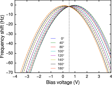
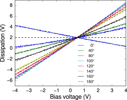
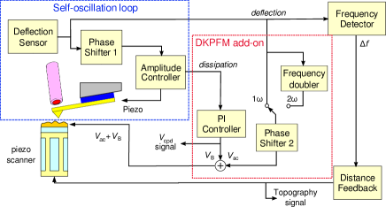
Figure 1 depicts the block diagram of the experimental setup used for both and D-KPFM measurements. The setup is based on the self-oscillation mode FM-AFM system Albrecht et al. (1991) and three additional components, a frequency doubler, a phase shifter, a proportional-integrator (PI) controller, are required for D-KPFM operation. The amplitude controller composed of a root-mean-square (RMS) amplitude detector and a PI controller is used to keep an oscillation amplitude constant. The output of the amplitude controller is the dissipation signal which is used for controlling . The detection bandwidth of the RMS amplitude detector is extended to about 3 kHz. In order to produce a sinusoidal ac voltage with two times the tip oscillation frequency, the sinusoidal deflection signal from the cantilever deflection sensor is first fed into a frequency doubler. Then the output of the frequency doubler passes through the additional phase shifter (Phase Shifter 2), which serves to adjust the phase of the ac voltage, . The dissipation signal acts as the input signal to the PI controller, which adjusts to maintain a constant dissipation equal to the value without applied, not .
We used a JEOL JSPM-5200 atomic force microscope for the experiments with the modifications described in Ref. Miyahara et al. (2015). An open source scanning probe microscopy control software GXSM was used for the control and data acquisition Zahl et al. (2010). A commercial silicon AFM cantilever (NSC15, MikroMasch) with a typical spring constant of about 28 N/m and resonance frequency of kHz was used in high-vacuum environment with the pressure of mbar.
In order to validate Eqs. 2 and 3, - and - curves were measured while a coherent sinusoidally oscillating voltage with , V (2 V and various phases, is superposed with .
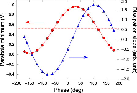
Figure 2(a) and (b) show simultaneously measured and versus curves, respectively. The curves are taken on a template stripped gold surface. A fitted curve with a parabola for each of the - curves (Eq. 2) or with a linear line for each of the - curves (Eq. 3) is overlaid on each experimental curve, indicating a very good agreement between the theory and experiments. As can be seen in Fig. 2(a) and (b), the position of the parabola vertex shifts both in and axes and the slope of - curve changes systematically with the varied phase, . For further validating the theory, the voltage coordinate of the parabola vertex (parabola minimum voltage) of each - curve and the slope of each - curve are plotted against in Fig. 3. Each plot is overlaid with a fitted curve (solid curve) with the cosine function (see Eq. 2) for the parabola minimum voltage and with the sine function (Eq. 3) for the dissipation slope, demonstrating an excellent agreement between the experiment and theory. The dependence of the frequency shift coordinate of the parabola vertices (frequency shift offset) also shows a very good agreement with the theory (second term of Eq. 2) (The fitting result is available in Supplemental Information). The parabola minimum voltage versus phase curve intersects that of - without ac bias voltage at . The deviation from the theoretically predicted value of 90∘ is due to the phase delay in the detection electronics. We also notice that the amplitude of parabola minimum versus phase curve is 0.472 V which is in good agreement with 0.5 V predicted by the theory ( in Eq. 2).
Figure 4 shows CPD images of a patterned MoS2 flake exfoliated on SiO2/Si substrate taken by (a)D-KPFM, (b)D-KPFM and (c)FM-KPFM techniques taken with the same tip. In () D-KPFM imaging, a sinusoidally oscillating voltage with (), mV ( V) and () coherent with the tip oscillation was applied to the sample. In FM-KPFM imaging, a sinusoidally oscillating voltage with Hz and V was applied to the sample. The detection bandwidth of the lock-in was 100 Hz. The scanning time for all the images were 1 s/line. A stripe pattern with 2 m pitch was created by reactive ion etching on the MoS2 flake. The topography images show an unetched terrace located between the etched regions (Image available in Supplemental Information.). The height of the unetched terrace is approximately 20 nm with respect to the etched regions. The bands shown in the middle of the CPD images corresponds to the unetched terrace and show a clear fractal-like pattern, which can be ascribed to the residue of the etch resist (PMMA). All three CPD images show apparently a very similar pattern on the terrace. However, a close inspection of the line profile of each image shows that D-KPFM and FM-KPFM provide a very similar potential profile with almost the same contrast while D-KPFM shows a potential contrast about two times smaller than that of D-KPFM and FM-KPFM. The close similarity between D-KPFM and FM-KPFM originates from the fact that (Eq. 3) is proportional to the force gradient as we have discussed above. Slightly larger potential contrast in D-KPFM compared with FM-KPFM is due to the faster feedback response of D-KPFM by virtue of the absence of low frequency modulation Miyahara et al. (2015), which is a clear advantage of both D-KPFM techniques over FM-KPFM. The bandwidth of FM-KPFM is limited by detection bandwidth of the lock-in amplifier that needs to be lower than the frequency of the ac bias voltage. The lower contrast of D-KPFM is ascribed to its sensitivity to electrostatic force rather than electrostatic force gradient which results in larger spatial average due to the stray capacitance including the body of the tip and the cantilever Hochwitz et al. (1996); Jacobs et al. (1998); Glatzel et al. (2003); Zerweck et al. (2005); Nomura et al. (2007).
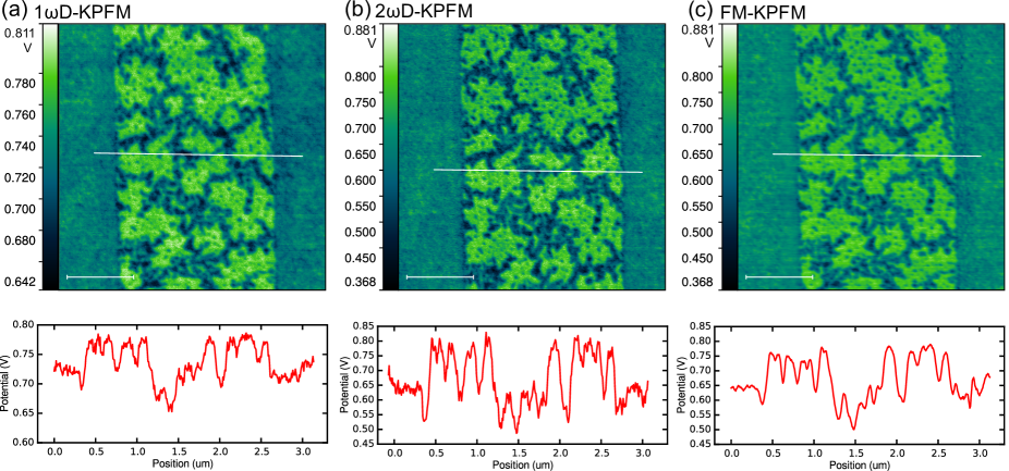
In spite of lower potential contrast, D-KPFM has an advantage that it requires much smaller mV compared with 1 V required in D-KPFM and FM-KPFM. This advantage is important for such samples as semiconductor where the influence of the large can be very important due to band-bending effects. As it is easy to switch between and D-KPFM modes, D-KPFM can be used for qualitative measurement with less electrical disturbance while D-KPFM can be used to obtain more accurate CPD contrast on the same sample location. Another advantage of D-KPFM is that it is free from the capacitive crosstalk to the piezoelectric element and photodiode signal line Diesinger et al. (2010) as the frequency of the ac voltage itself does not match any resonance of the cantilever.
In conclusion, we report a new technique that enables force-gradient sensitive Kelvin probe force microscopy using the dissipation signal of FM-AFM for dc voltage feedback. It features the simpler implementation and faster scanning as it requires no low frequency modulation. The dissipation is caused by the oscillating electrostatic force that is coherent with the tip oscillation, which is induced by applying a sinusoidally oscillating ac voltage with the frequency two times that of the tip oscillation frequency. We theoretically analyzed the effect of the applied ac voltage and show that the induced dissipation is sensitive to electrostatic force gradient rather than electrostatic force. The experiments confirmed the theoretical analysis and demonstrated that D-KPFM provides essentially the same result obtained by FM-KPFM. The combination of and D-KPFM techniques will be a versatile tool to study the samples whose electrical properties are sensitive to the external electric field.
The authors would like to thank Dr. Omid Salehzadeh Einabad and Prof. Zetian Mi at McGill University for providing the MoS2 sample. This work was partly supported by the Natural Science and Engineering Research Council (NSERC), le Fonds Québécois de Recherche sur la Nature et les Technologies (FQRNT).
References
References
- Miyahara et al. (2015) Y. Miyahara, J. Topple, Z. Schumacher, and P. Grutter, Physical Review Applied 4, 054011 (2015).
- Nonnenmacher et al. (1991) M. Nonnenmacher, M. P. O’Boyle, and H. K. Wickramasinghe, Appl. Phys. Lett. 58, 2921 (1991).
- Kitamura et al. (2000) S. Kitamura, K. Suzuki, M. Iwatsuki, and C. B. Mooney, Appl. Surf. Sci. 157, 222 (2000).
- L N Kantorovich et al (2000) L N Kantorovich et al, J. Phys. Condens. Matter 12, 795 (2000).
- Labuda et al. (2012) A. Labuda, K. Kobayashi, Y. Miyahara, and P. Grütter, Rev. Sci. Instrum. 83, 053703 (2012).
- Hölscher et al. (2001) H. Hölscher, B. Gotsmann, W. Allers, U. Schwarz, H. Fuchs, and R. Wiesendanger, Phys. Rev. B 64, 075402 (2001).
- Kantorovich and Trevethan (2004) L. N. Kantorovich and T. Trevethan, Phys. Rev. Lett. 93, 236102 (2004).
- Sader et al. (2005) J. E. Sader, T. Uchihashi, M. J. Higgins, A. Farrell, Y. Nakayama, and S. P. Jarvis, Nanotechnology 16, S94 (2005).
- Sugawara et al. (2012) Y. Sugawara, L. Kou, Z. Ma, T. Kamijo, Y. Naitoh, and Y. Jun Li, Appl. Phys. Lett. 100, 223104 (2012).
- Nomura et al. (2007) H. Nomura, K. Kawasaki, T. Chikamoto, Y. J. Li, Y. Naitoh, M. Kageshima, and Y. Sugawara, Appl. Phys. Lett. 90, 033118 (2007).
- Fukuma et al. (2004) T. Fukuma, K. Kobayashi, H. Yamada, and K. Matsushige, Rev. Sci. Instrum. 75, 4589 (2004).
- Albrecht et al. (1991) T. R. Albrecht, P. Grutter, D. Horne, and D. Rugar, J. Appl. Phys. 69, 668 (1991).
- (13) For convenience, HF2LI lock-in amplifier (Zurich Instruments) in external reference mode was used as a frequency doubler as well as phase shifter.
- Zahl et al. (2010) P. Zahl, T. Wagner, R. Möller, and A. Klust, J. Vac. Sci. Technol. B Nanotechnol. Microelectron. 28, C4E39 (2010).
- Hochwitz et al. (1996) T. Hochwitz, A. K. Henning, C. Levey, and C. Daghlian, J. Vac. Sci. Technol. B Nanotechnol. Microelectron. 14, 457 (1996).
- Jacobs et al. (1998) H. O. Jacobs, P. Leuchtmann, O. J. Homan, and A. Stemmer, J. Appl. Phys. 84, 1168 (1998).
- Glatzel et al. (2003) T. Glatzel, S. Sadewasser, and M. Lux-Steiner, Appl. Surf. Sci. 210, 84 (2003).
- Zerweck et al. (2005) U. Zerweck, C. Loppacher, T. Otto, S. Grafstrom, and L. M. Eng, Phys. Rev. B 71, 125424 (2005).
- Diesinger et al. (2010) H. Diesinger, D. Deresmes, J.-P. Nys, and T. Mélin, Ultramicroscopy 110, 162 (2010).