Tailoring supercurrent confinement in graphene bilayer weak links
The Josephson effect is one of the most studied macroscopic quantum phenomena in condensed matter physics and has been an essential part of the quantum technologies development over the last decades. It is already used in many applications such as magnetometry, metrology, quantum computing, detectors or electronic refrigeration. However, developing devices in which the induced superconductivity can be monitored, both spatially and in its magnitude, remains a serious challenge. In this work, we have used local gates to control confinement, amplitude and density profile of the supercurrent induced in one-dimensional nanoscale constrictions, defined in bilayer graphene-hexagonal boron nitride van der Waals heterostructures. The combination of resistance gate maps, out-of-equilibrium transport, magnetic interferometry measurements, analytical and numerical modelling enables us to explore highly tunable superconducting weak links. Our study opens the path way to design more complex superconducting circuits based on this principle such as electronic interferometers or transition-edge sensors.
Superconductivity can be induced in a material by direct contact to a superconductor. This proximity effect allows the transmission of Andreev pairs from a superconducting electrode to another when these are close enough. The Josephson effect can then be measured as it is observed in tunnel junctions Josephson1962 ; Anderson1963 ; tinkhambook . However, the tuning of the dissipationless current in such Josephson junctions is not possible without changing its geometry or temperature. By replacing the tunnel junction by a so-called weak link Likharev1979 ; BaronePaternoBook , i.e. any kind of conductive system, the supercurrent may flow over a much larger distance than the couple of nanometers of a tunnel barrier. The magnitude of the supercurrent mainly depends on the contact transparency, the disorder in the weak link and the temperature Likharev1979 .
Many different types of materials and systems have been used as weak links, ranging from mesoscopic diffusive metallic wires Baselmans1999 , two-dimensional (2D) electron gas Schaepers2003 , graphene Heersche2007 , topological insulators Zhang2011 ; Sacepe2011 ; Veldhorst2012 ; Oostinga2013 ; Hart2014 ; Bocquillon2016 and quantum dots DeFranceschi2010 , as well as atomic contacts Goffman2000 . When graphene is utilised as a weak link, the Josephson effect can be tuned by electrostatic gating Heersche2007 ; Du2008 ; Miao2009 ; Rickhaus2012 ; Coskun2012 ; Komatsu2012 ; Mizuno2013 ; Choi2013 and, thanks to edge connection which provides very low contact resistance Wang2013 , it is possible to measure large supercurrent as well as ballistic interferences Calado2015 ; BenShalom2016 ; Allen2016 ; Amet2016 ; Borzenets2016 . However, in spite of these excellent predispositions to mediate superconductivity, a full control of the supercurrent both in its amplitude and spatial distribution has not been demonstrated up to now. One of the reasons behind this is the difficulty to confine charge carriers in graphene due to the absence of back scattering and Klein tunnelling katsnelsonbook . The use of bilayer graphene (BLG) could circumvent these problems since it is possible to engineer an electronic band gap by breaking the lattice inversion symmetry of the AB-stacked bilayer McCann2006 ; McCannKoshino2013 . Indeed, by means of local gating, BLG can provide a way to shape the supercurrent distribution and allow a complete monitoring of proximity induced superconductivity. In this work, we have used edge connected BLG-hexagonal boron nitride (hBN) heterostructures as a medium for induced superconductivity, and use a quantum point contact (QPC)-like geometry to study supercurrent confinement.
I How to read a dual gate map: Inducing a 1D constriction
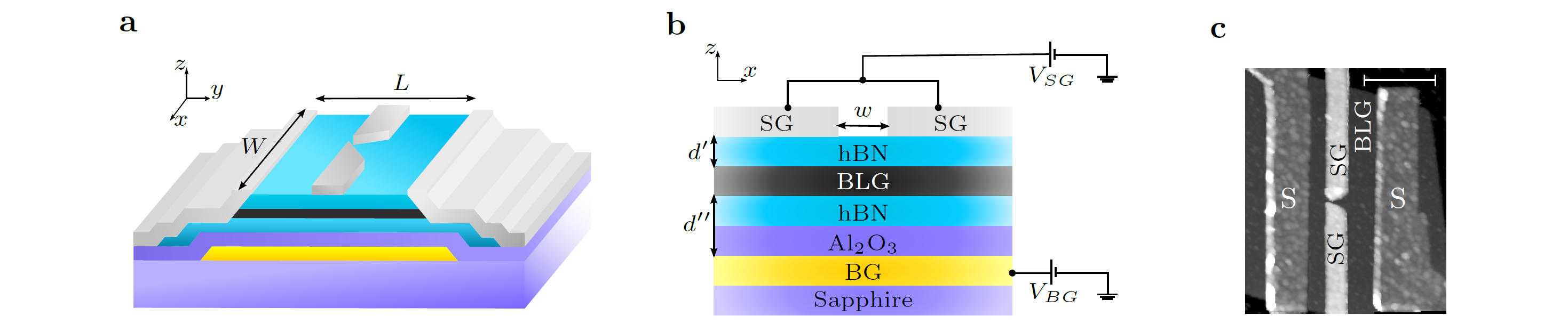
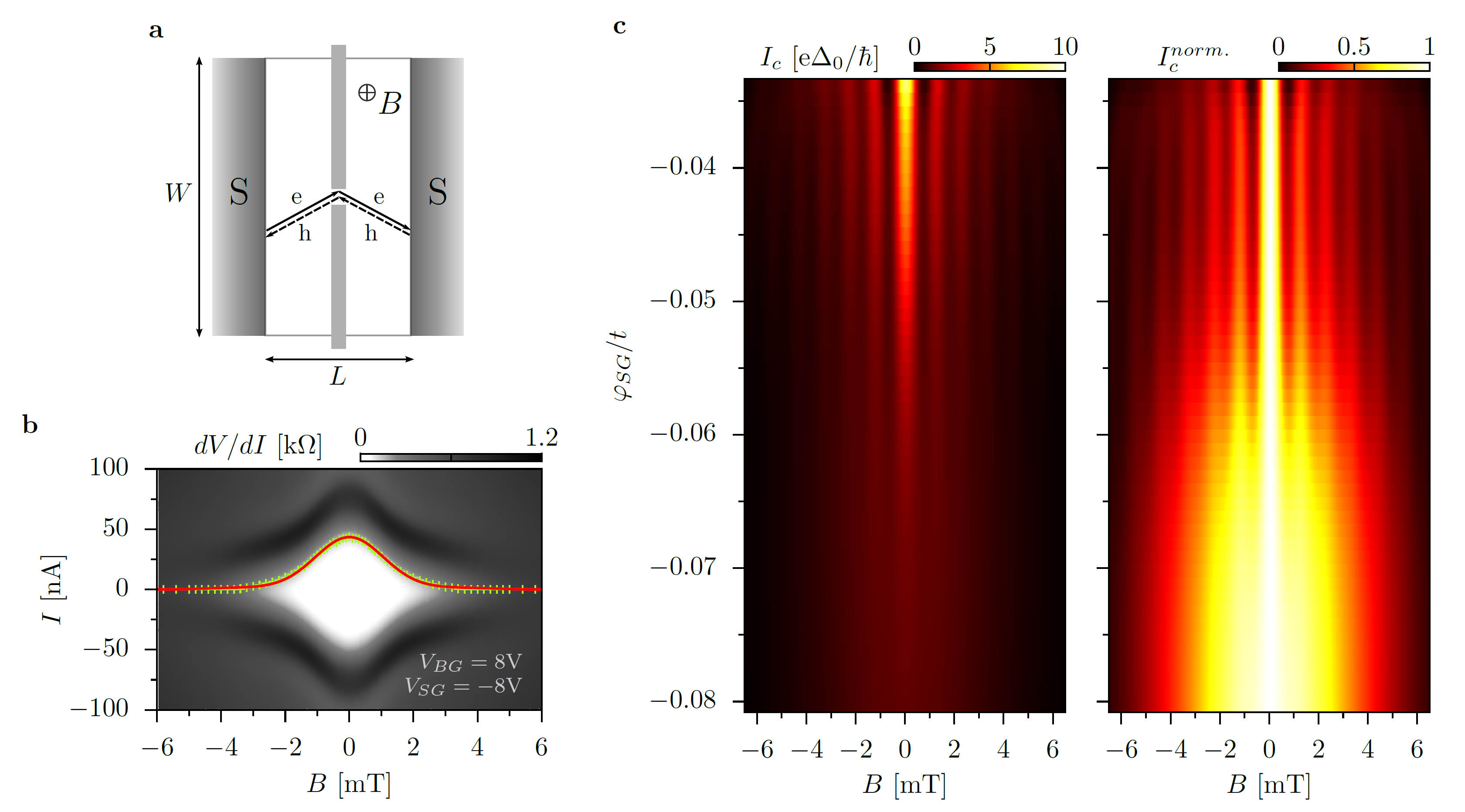
The sample geometry used in this study is depicted in Fig. 1. Following the fabrication method of Wang et al. Wang2013 , we employ BLG encapsulated between hBN multilayers connected from the edge of the mesa with superconducting titanium/aluminium electrodes. The constriction is realised by inducing displacement fields between an overall pre-patterned back-gate and a local top-gate designed in a QPC-like split-gate geometry (see Fig. 1). Two devices were measured which show similar behaviour, here we present the data based on the shortest sample (details on the sample fabrication are presented in the supplementary information).
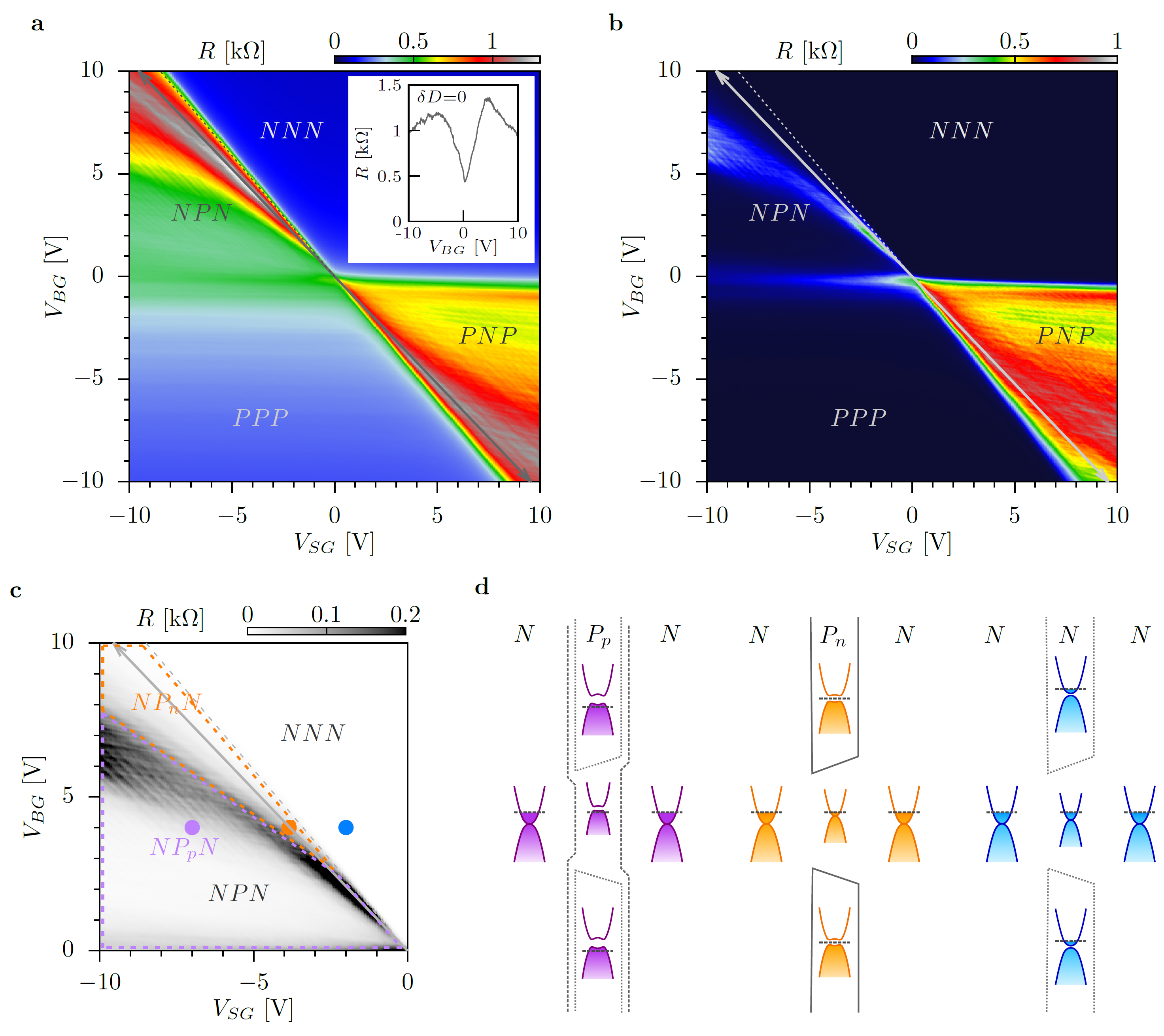
The normal state characteristics of our sample show a residual charge carrier density as low as cm-2, well developed Landau fans in magnetotransport experiments as well as multiple Fabry-Pérot interferences generated by the charge carriers travelling back and forth within the several cavities formed in our system (see supplementary information for the full analysis). Figures 2a and 2b display resistance maps as a function of split- and back-gate voltage measured in the normal and superconducting state respectively (i.e. at 20 mT and zero magnetic field). In both cases, distinct deviations from the expected quadrants formed in lateral -junctions corresponding to the differently doped regions Oostinga2007 ; Taychatanapat2010 ; Varlet2014 are clearly visible (unipolar and bipolar regions , and , respectively).
In BLG dual-gated devices, the displacement field is used to break the lattice inversion symmetry of the AB-stacked bilayer: the two layers being at different potentials a band gap opens McCann2006 ; McCannKoshino2013 , inducing an insulating state with strongly suppressed conductivity. The resistance then raises monotonically with increasing displacement field as the band gap develops Oostinga2007 ; Taychatanapat2010 ; Varlet2014 . Here, we observe a non-monotonic change of the resistance which first increases and then drops after reaching a maximum while following the displacement field line (i.e. when the displacement field generated by the back- and split-gates, respectively and are equal, at Zhang2009 ). In addition, the resistance peak does not follow the displacement field line which is indicated by the gray arrow as depicted in Fig. 2a and 2b, but diverges into the bipolar regions ( and ). This trend is already noticeable in the normal state resistance (Fig. 2a), but becomes strikingly evident in the superconducting state (Fig. 2b). This unexpected behaviour can be understood as the competitive action of back- and split-gates within the constriction. As the displacement field increases, the charge carrier density mostly driven by the back-gate becomes less and less affected by the stray fields developed by the split-gate which cannot compensate the influence of the back-gate on the channel region. Consequently, the device remains highly conductive in contrast to the pinch-off characteristic of gapped BLG with full-width top-gate. Instead, the maximum resistance deviates from the displacement field line and “bends”. The bent line of the resistance peak results then from the required overcompensation of the split-gate voltage to diminish the induced charge carriers within the channel region. Instead of being maximum along the displacement field line Oostinga2007 ; Taychatanapat2010 ; Varlet2014 (marked as a diagonal arrowed line on the gate maps), the resistance increases up to a maximum then decreases as plotted in the inset of Fig. 2a. However, this imbalance between applied split- and back-gate voltages starts to induce charge carriers of opposite sign in the dual-gated cavities, resulting in -junctions. As a consequence, the bipolar regions become then subdivided into two parts depending on the doping in the constriction (denoted by a sub-label like , see Fig. 2c). The QPC-like structure can then be driven in an “open” (the 1D channel doping is of the same type as the 2D reservoirs) or “closed” (the 1D channel doping is of opposite type as the reservoirs forming a non-uniform potential barrier) regime.
The schematics in Fig. 2d summarize the different scenarios which govern the behaviour of such an electrostatically induced constriction. It is important to note that the overall resistance remains higher on the -side ( and ) due to the slight -doping provided by the leads which create a -junction at each contact. This becomes particularly clear in the superconducting state where the region remains resistive while a large part of the section displays a zero resistance state. For this reason, we focus on the area and in particular on the part where we can study the supercurrent flowing through the constriction.
II Supercurrent analysis
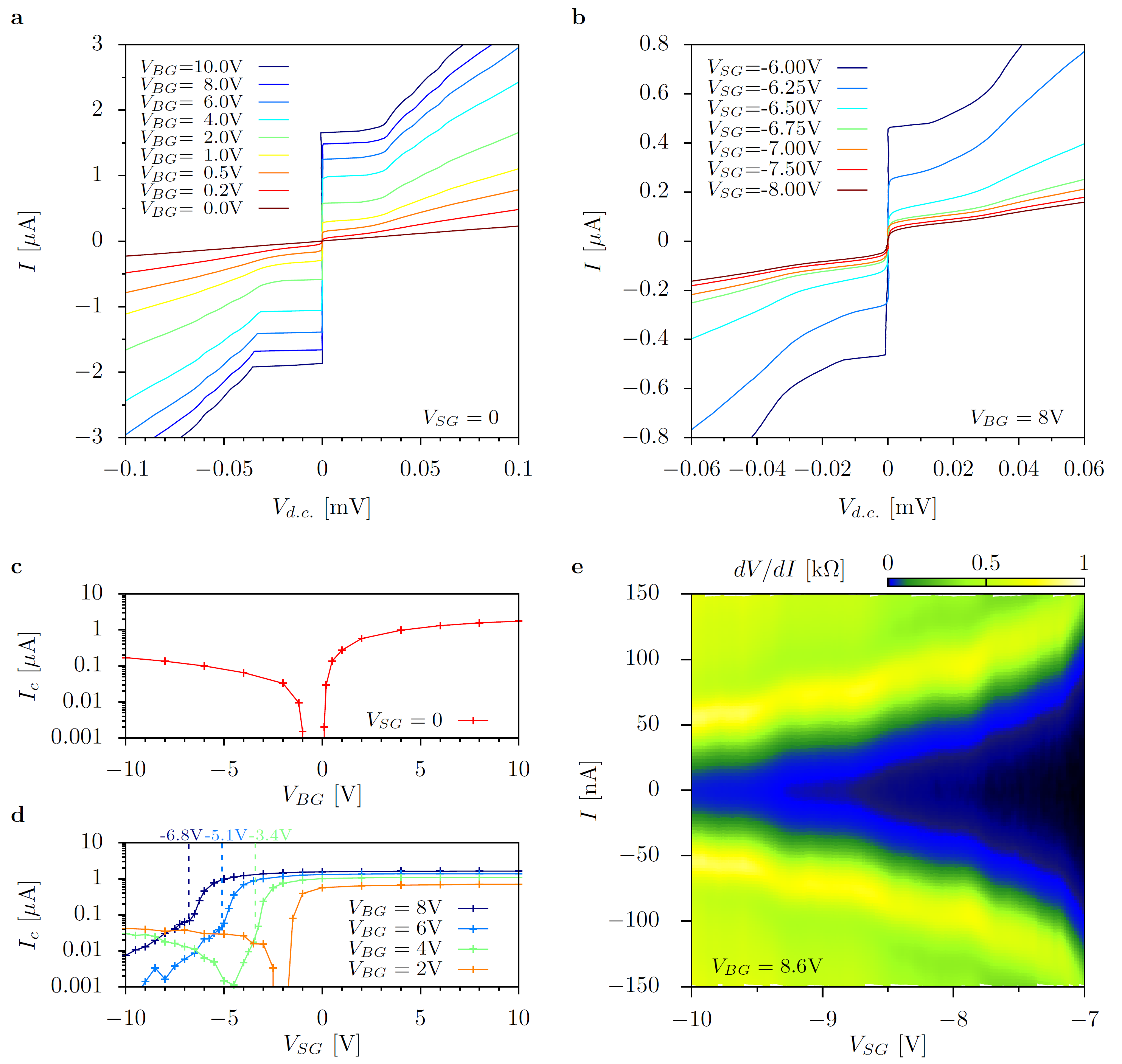
Now we describe how to control both supercurrent amplitude and spatial distribution using our split-gate geometry. We have seen in the previous section that our device becomes superconducting in the area where the constriction is formed, namely the region. One way to verify our hypothesis consists of probing the critical current which corresponds to the maximum supercurrent that a weak link can support before switching to a resistive state (see method section for a description of the critical current extraction procedure and the supplementary information for details). being extremely sensitive to any external perturbations such as magnetic field, potential landscape inhomogeneities or thermal excitation, drastic changes of the confinement should be clearly observed. Indeed, the variation of the normal state resistance is directly reflected in the supercurrent amplitude. For example, small oscillations in the resistance produced by Fabry-Pérot interferences are directly detected in the supercurrent Jorgensen2006 ; Calado2015 ; BenShalom2016 ; Borzenets2016 (see supplementary information). Here, we focus our attention on the effect of the 1D constriction on the supercurrent amplitude.
The amplitude of the supercurrent can be monitored by tuning the charge carrier density with the overall back-gate voltage . In Fig. 3a the current-voltage characteristics are shown in the absence of a constriction, i.e. for a uniform 2D weak link at . The supercurrent evolves from zero at the charge neutrality point up to a measured maximum of A at high charge carrier density cm-2 (i.e. V). It is important to note that the I-V characteristics only display a rather limited hysteretic behaviour visible only at large charge carrier density corresponding to a weakly underdamped junction within the resistively and capacitively shunted junction (RCSJ) model tinkhambook . When the Fermi level lies in the valence band (), the weak link is disturbed by the presence of the -junctions which strongly suppresses the supercurrent by an order of magnitude (approximately 200 nA at V). This is clearly seen in Fig. 3c where the critical current is plotted as a function of the back-gate voltage .
Fig. 3b displays a series of I-V curves at fixed charge carrier density (here at V) for different split-gate values in the vicinity of the area. When approaching the formation of the constriction, decreases rapidly until V. At this point, the Fermi level underneath the split-gate is positioned in the gap. Therefore, charge carriers can only flow through the 1D constriction. Beyond the formation of the constriction, decreases in a much slower fashion. The extracted critical current is plotted in Fig. 3d as a function of the split-gate voltage at different densities. At small densities, i.e. V (orange curve in Fig. 3d), the starting point of the region appears early in gate voltage and the supercurrent is switched off. Then, the Fermi level in the constriction which remains mainly driven by the stray fields of the split-gate moves towards the valence band. Due to the close proximity of the split-gates, the stray fields are strong enough to close the channel. A small supercurrent can be detected despite the presence of a weak -junction as depicted in Fig. 2d ( area). In contrast, at higher densities the back-gate starts to electrostatically dominate the constriction region. The creation of the 1D channel is directly reflected in the sudden change of slope of curves (blue and dark blue curves in Fig. 3d, the change of slope being marked by dotted lines). The supercurrent through the channel is then only slowly reduced with increasing split-gate voltage owing to the narrowing of the channel by the stray fields. Once the channel is created, the amplitude of the supercurrent drops way below 100 nA while multiple Andreev reflections completely vanish (see supplementary information). At intermediate density (green curve in Fig. 3d), the channel is first created (rapid drop in then change of slope marked by the dotted curve), then closed with the Fermi level positioned in the gap (supercurrent switched off), to finally form a non-uniform -junction as depicted in Fig. 2d ( area). Importantly, despite the absence of signs of 1D subband formation while shrinking the constriction in the normal state, the critical current decreases in a step-wise fashion (see Fig. 3e) as predicted for ballistic supercurrents in quantum point contacts Furasaki1991 ; Furasaki1992 ; Takayanagi1995 .
III Magneto-interferometry
The supercurrent density distribution across the sample width can be explored by probing its interference pattern Rowell1963 in response to a perpendicular magnetic flux penetrating the junction DynesFulton1971 ; Zappe1975 ; BaronePaternoBook ; Barzykin1999 ; Kikuchi2000 ; Angers2008 ; Chiodi2012 ; Amado2013 ; Hart2014 ; Allen2016 . Therefore, by changing the geometry of the system one can observe a large variety of interference patterns directly related to the supercurrent density distribution BaronePaternoBook . As recently shown Hart2014 ; Allen2016 , superconducting interferometry is a powerful tool to probe confinement where the current density distribution can be extracted by complex Fourier transform following the approach of Dynes and Fulton DynesFulton1971 . However, this technique of recovering the supercurrent assumes that it is carried strictly in a direction normal to the superconducting electrodes, and therefore does not apply to our device because of its small aspect ratio, especially in the QPC regime.
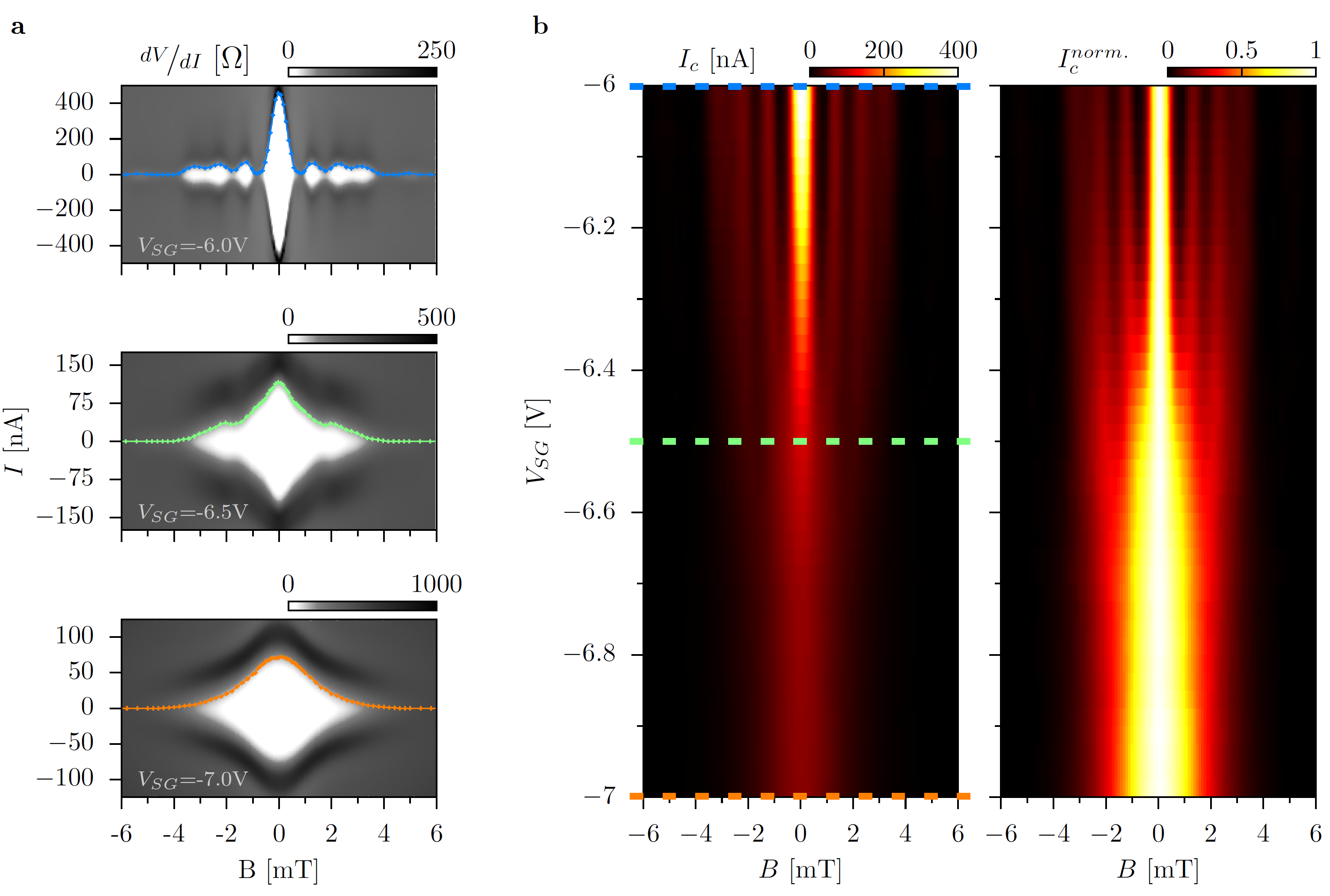
Here, we show that the magnetic interference pattern indicates clear signatures of the supercurrent confinement. Fig. 4a exhibits a series of resistance maps versus current and magnetic field at constant density (V). A progressive change of the interference pattern is observed as the split-gate is tuned and the 1D constriction forms. First, a beating pattern appears, resembling Fraunhofer-like interference (upper panel) when the system remains two-dimensional. Then the interference pattern turns to a “lifting lobes” shape just before the formation of the constriction (middle panel). Finally a non-beating “bell-shaped” pattern is formed while the supercurrent flows only through the confined 1D constriction (lower panel). We note that the transition from a beating to a non-beating pattern occurs on a rather narrow voltage range -7 V -6 V (at V, additional data at V are shown in the supplementary information). In Fig. 4b we can observe a map of the critical current (left panel) as well as the critical current normalized with the maximum critical current (at ) (right panel) as a function of magnetic field and split-gate voltage , allowing a more accurate vision of the transition from 2D (beating pattern) to 1D (“bell-shaped” pattern). Each horizontal slice of such maps corresponds to the extracted critical current (or normalized critical current) of a single magnetic interference pattern. We note that such non-beating pattern has been observed in rectangular superconducting weak links with low aspect ratio Angers2008 ; Chiodi2012 ; Amado2013 . From the magneto-interferometry experiments, no obvious signs of induced current through topological channels appearing due to AB stacking faults Ju2015 or edge states Allen2016 ; Zhu2017 have been detected.
In order to gain deeper understanding how the magnetic interferences should evolve with the creation of a 1D constriction into a 2D system, we have designed an analytical model where we calculate the Josephson current through the sample in the presence of a magnetic field (see supplementary information for details), using a quasi-classical approach (as in Barzykin1999 ; Sheehy2003 ; Meier2016 ) with an additional input given by the presence of a QPC-like structure in the middle of the device (see the geometry used in Fig. 5a). We have used our analytic expression to fit the maximum critical current as a function of magnetic field (see Fig. 5b). The theoretical critical current (red curve) is matched to the experimental data (green crosses) by scaling the curve by a factor of the extracted maximum critical current nA using a junction area of m2 with a total junction length of m where is the London penetration depth (nm). Our model follows clearly the experimental data which, once again, proves that the supercurrent has been strongly confined in our quantum point contact edge connected BLG. We finally show tight-binding simulations using Kwant package Groth14 of as a function of magnetic field and split-gate strength in Fig. 5c (see supplementary information for details) which are in good qualitative agreement with our experimental data of Fig. 4c.
IV Conclusion and perspectives
In this work, we have demonstrated a full monitoring, both spatially and in amplitude, of the supercurrent in a clean and edge connected hBN-BLG-hBN heterostructure. In a split-gate geometry we have explored the consequences of the 1D confinement on the supercurrent and on its magnetic interferences. Thanks to in turn, the possibility to locally engineer an electronic band gap in BLG, the injection of a large and fully tunable critical current, and the ultra-low disorder of fully encapsulated hBN-BLG-hBN heterostructures, we have designed a unique platform allowing the creation of new types of superconducting circuits based on fully tunable weak links which can be controlled by the combination of top- and back-gates.
References
- (1) Josephson, B.D. Possible new effects in superconductive tunneling. Phys. Lett. 1, 251-253 (1962).
- (2) Anderson, P.W., & J.M. Rowell. Probable Observation of the Josephson Superconducting Tunneling Effect. Phys. Rev. Lett. 10, 230-232 (1963).
- (3) Tinkham, M. Introduction to Superconductivity (Courier Dover, 2012).
- (4) Likharev, K.K. Superconducting weak links. Rev. Mod. Phys. 51, 101-159 (1979).
- (5) Barone, A. & Paterno, G. Physics and Applications of the Josephson Effect (John Wiley, 1982).
- (6) Baselmans, J.J.A., Morpurgo, A.F., van Wees, B.J., & Klapwijk, T.M. Reversing the direction of the supercurrent in a controllable Josephson junction. Nature 397, 43-45 (1999).
- (7) Schäpers, T. Superconductor/Semiconductor Junctions (Springer, 2003).
- (8) Heersche, H. B., Jarillo-Herrero, P., Oostinga, J. B., Vandersypen, L. M. K. & Morpurgo, A. F. Bipolar supercurrent in graphene. Nature 446, 56-59 (2007).
- (9) Zhang, D., Wang, J., DaSilva, A.M., Lee, J.S., Gutierrez, H.R., Chan, M.H.W., Jain, J., & Samarth, N. Superconducting proximity effect and possible evidence for Pearl vortices in a candidate topological insulator. Phys. Rev. B 84, 165120 (2011).
- (10) Sacépé, B., Oostinga, J.B., Li, J., Ubaldini, A., Couto, N.J.G. , Giannini, E., & Morpurgo, A.F. Gate-tuned normal and superconducting transport at the surface of a topological insulator. Nature Commun. 2, 575 (2011).
- (11) Veldhorst, M., Snelder, M., Hoek, M., Gang, T., Guduru, V.K., Wang, X.L., Zeitler, U., van der Wiel, W.G., Golubov, A.A., Hilgenkamp, H., & Brinkman, A. Josephson supercurrent through a topological insulator surface state. Nature Mater. 11, 417-421 (2012).
- (12) Oostinga, J.B., Maier, L., Schüffelgen, Knott, P.D., Ames, C., Brüne, C., Tkachov, G., Buhmann, H., & Molenkamp, L.W. Josephson supercurrent through the topological surface states of strained bulk HgTe. Phys. Rev. X 3, 021007 (2013).
- (13) Hart, S., Ren, H., Wagner, T., Leubner, P., Mühlbauer, M., Brüne, C., Buhmann, H., Molenkamp, L.W. & Yacoby, A. Induced superconductivity in the quantum spin Hall edge. Nature Phys. 10, 638-643 (2014).
- (14) Bocquillon, E., Deacon, R.S., Wiedenmann, J., Leubner P. , Klapwijk, T.M., Brüne, C., Ishibashi, K., Buhmann H., & Molenkamp, L.W. Gapless Andreev bound states in the quantum spin Hall insulator HgTe. Nature Nanotech. 12, 137-143 (2017).
- (15) De Franceschi, S., Kouwenhoven, L., Schönenberger, C., & Wernsdorfer, W. Hybrid superconductor–quantum dot devices. Nature Nanotechnol. 5, 703-711 (2010).
- (16) Goffman, M.F., Cron, R., Levy Yeyati, A., Joyez, P., Devoret, M.H., Esteve, D. & Urbina, C. Supercurrent in Atomic Point Contacts and Andreev States. Phys. Rev. Lett. 85, 170-173 (2000).
- (17) Du, X., Skachko, I. & Andrei, E.Y. Josephson current and multiple Andreev reflections in graphene SNS junctions. Phys. Rev. B 77, 184507 (2008).
- (18) Miao, F., Bao, W., Zhang, H. & Lau, C.N. Premature switching in graphene Josephson transistors. Solid State Commun. 149, 1046-1049 (2009).
- (19) Rickhaus, P., Weiss, M., Marot, L. & Schönenberger, C. Quantum Hall effect in graphene with superconducting electrodes. Nano Lett. 12, 1942-1945 (2012).
- (20) Coskun, U.C., Brenner, M., Hymel, T., Vakaryuk, Levchenko, V.A. & Bezryadin, A. Distribution of supercurrent switching in graphene under proximity effect. Phys. Rev. Lett. 108, 097003 (2012).
- (21) Komatsu, K., Li, C., Autier-Laurent, S., Bouchiat, H. & Gueron, S. Superconducting proximity effect through graphene from zero field to the quantum Hall regime. Phys. Rev. B 86, 115412 (2012).
- (22) Mizuno, N., Nielsen, B. & Du, X. Ballistic-like supercurrent in suspended graphene Josephson weak links. Nature Commun. 4, 2716 (2013).
- (23) Choi, J.-H., G.-H. Lee, S. Park, D. Jeong, J.-O Lee, H.-S. Sim, Y.-J. Doh, & H.-J. Lee. Complete gate control of supercurrent in graphene junctions. Nature Commun. 4, 2525 (2013).
- (24) Wang, L., Meric, I., Huang, P.Y., Gao, Q., Gao, Y., Tran, H., Taniguchi, T., Watanabe, K., Campos, L.M., Muller, D.A., Guo, J., Kim, P., Hone, J., Shepard, K.L., & Dean, C.R. One-dimensional electrical contact to a two-dimensional material. Science 342, 614-617 (2013).
- (25) Calado, V.E., Goswami, Nanda, S.G., Diez, M., Akhmerov, A.R., Watanabe, K., Taniguchi, T., Klapwijk, T.M. & Vandersypen, L.M.K. Ballistic Josephson junctions in edge-contacted graphene. Nature Nanotech. 10, 761-764 (2015).
- (26) Ben Shalom, M., Zhu, M.J., Fal’ko, V.I., Mishchenko, A., Kretinin, A.V., Novoselov, K.S., Woods, C.R., Watanabe, K., Taniguchi, T., Geim, A.K. & Prance, J.R. Quantum oscillations of the critical current and high-field superconducting proximity in ballistic graphene. Nature Phys. 12, 318-322 (2016).
- (27) Allen, M.T., Shtanko, O., Fulga, I.C., Akhmerov, A.R., Watanabe, K., Taniguchi, T., Jarillo-Herrero, P., Levitov, L.S. & Yacoby, A. Spatially resolved edge currents and guided-wave electronic states in graphene. Nature Phys. 12, 128-133 (2016).
- (28) Amet, F., Ke, C.T., Borzenets, I.V., Wang, J., Watanabe, K., Taniguchi, T., Deacon, R.S., Yamamoto, M., Bomze, Y., Tarucha, S. & Finkelstein, G. Supercurrent in the quantum Hall regime. Science 352, 966-969 (2016).
- (29) Borzenets, I.V., Amet, F., Ke, C.T., Draelos, A.W., Wei, M.T., Seredinski, A., Watanabe, K., Taniguchi, T., Bomze, Y., Yamamoto, M., Tarucha, S. & Finkelstein G. Ballistic graphene Josephson junctions from the short to the long junction regimes. Phys. Rev. Lett. 117, 237002 (2016).
- (30) Katsnelson, M.I. Graphene. Carbon in Two Dimensions (Cambridge University Press, 2012).
- (31) McCann, E. Asymmetry gap in the electronic band structure of bilayer graphene. Phys. Rev. B 74, 161403 (2006).
- (32) McCann, E. & Koshino, M. The electronic properties of bilayer graphene. Rep. Progr. Phys. 76, 056503 (2013).
- (33) Oostinga, J. B., Heersche, H. B., Liu, X., Morpurgo, A. F. & Vandersypen, L. M. K. Gate-induced insulating state in bilayer graphene devices. Nature Mater. 7, 151-157 (2007).
- (34) Taychatanapat, T. & Jarillo-Herrero, P. Electronic transport in dual-gated bilayer graphene at large displacement fields. Phys. Rev. Lett. 105, 166601 (2010).
- (35) Varlet, A., Liu, M.-H., Krueckl, V., Bischoff, D., Simonet, P., Watanabe, K., Taniguchi, T., Richter, K., Ensslin, K. & Ihn, T. Fabry-Pérot interference in gapped bilayer graphene with broken anti-Klein tunneling. Phys. Rev. Lett. 113, 116601 (2014).
- (36) Zhang, Y. Tang, T.-T., Girit, C., Hao, Z., Martin, M.C., Zettl, A., Crommie, M.F., Shen, Y.R. & Wang, F. Direct observation of a widely tunable bandgap in bilayer graphene. Nature 459, 820-823 (2009).
- (37) Jørgensen, H.I., Grove-Rasmussen, K., Novotný, T., Flensberg, K. & Lindelof, P.E. Electron transport in single-wall carbon nanotube weak links in the Fabry-Pérot regime. Phys. Rev. Lett. 96, 207003 (2006).
- (38) Furusaki, A., Takayanagi, H. & Tsukada, M. Theory of Quantum Conduction of Supercurrent through a Constriction. Phys. Rev. Lett. 67, 132-135 (1991).
- (39) Furusaki, A. Josephson effect of the superconducting quantum point contact. Phys. Rev. B 45, 10563-10575 (1992).
- (40) Takayanagi, H., Akazaki, T. & Nitta, J. Observation of maximum supercurrent quantization in a superconducting quantum point contact. Phys. Rev. Lett. 75, 3533-3536 (1995).
- (41) Rowell, J.M. Magnetic field dependence of the Josephson tunnel current. Phys. Rev. Lett. 11, 200-202 (1963).
- (42) Dynes, R. C. & Fulton, T. A. Supercurrent density distribution in Josephson junctions. Phys. Rev. B 3, 3015-3023 (1971).
- (43) Zappe, H.H. Determination of the current density distribution in Josephson tunnel junctions. Phys. Rev. B 7, 2535-2538 (1975).
- (44) Barzykin, V. & Zagoskin, A. M. Coherent transport and nonlocality in mesoscopic SNS junctions: anomalous magnetic interference patterns. Superlat. Microstruct. 25, 797-807 (1999).
- (45) Kikuchi, K., Myoren, H., Iizuka, T. & Takada, S. Normal-distribution-function-shaped Josephson tunnel junctions. Appl. Phys. Lett. 77, 3660-3661 (2000).
- (46) Angers, L., Chiodi, F., Montambaux, G., Ferrier, M., Guéron, S., Bouchiat, H. & Cuevas., J.C. Proximity dc squids in the long-junction limit. Phys. Rev. B 77, 165408 (2008).
- (47) Chiodi, F., Ferrier, M., Guéron, S., Cuevas, J.C., Montambaux, G., Fortuna, F., Kasumov, A. & Bouchiat, H. Geometry-related magnetic interference patterns in long SNS Josephson junctions. Phys. Rev. B 86, 064510 (2012).
- (48) Amado, M., Fornieri, A., Carillo, F., Biasiol, G., Sorba, L., Pellegrini, V., & Giazotto, F. Electrostatic tailoring of magnetic interference in quantum point contact ballistic Josephson junctions. Phys. Rev. B 87, 134506 (2013).
- (49) Ju, L., Shi, Z., Nair, N., Lv, Y., Jin, C., Velasco Jr., J., Ojeda-Aristizabal, C., Bechtel, H.A., Martin, M.C., Zettl, A., Analytis, J. & Wang., F. Topological valley transport at bilayer graphene domain walls. Nature 520, 650 (2015).
- (50) Zhu, M.J., Kretinin, A.V., Thompson, M.D., Bandurin, D.A., Hu, S., Birkbeck, J., Mishchenko, A., Vera-Marun, I.J., Watanabe, K., Taniguchi, T., Polini, M. Prance, J.R., Novoselov, K.S., Geim, A.K. & Ben Shalom, M. Edge currents shunt the insulating bulk in gapped graphene. Nature Commun. 8, 14552 (2017).
- (51) Sheehy, D.E. & Zagoskin, A.M. Theory of anomalous magnetic interference pattern in mesoscopic superconducting/normal/superconducting Josephson junctions. Phys. Rev. B 68, 144514 (2003).
- (52) Meier, H., Fal’ko,V.I. & Glazman, L.I. Edge effects in the magnetic interference pattern of a ballistic SNS junction. Phys. Rev. B 93, 184506 (2016).
- (53) Groth, C. W., Wimmer, M., Akhmerov, A.R. & Waintal, X. Kwant: a software package for quantum transport, New J. Phys. 16, 063065 (2014).
Acknowledgements
The authors thank A. Mirlin, M. Titov and W. Wernsdorfer for fruitful discussions. This work was partly supported by Helmholtz society through program STN and the DFG via the projects DA 1280/3-1 and GO 1405/3-1.
A.A. and M.I. acknowledge support of the European Research Council, and the Netherlands Organisation for Scientific Research (NWO/OCW), as part of the Frontiers of Nanoscience program.
Author contributions
R.Kra. performed the experiments with the support of J.M., R.Du., P.B.S., F.W. and R.Da. R.Kra. fabricated the devices with the support of J.M. U.N.K. and I.G. designed the analytical model. M.I. and A.A. performed the numerical calculations. All authors discussed about the results. R.Da. and R.Kra. performed the data analysis and wrote the paper. R.Da. designed and planned the experiments.
Additional information
Correspondence and requests for materials should be addressed to R.Da. (e-mail: romain.danneau@kit.edu)
Competing financial interests
The authors declare no competing financial interests.
IV.1 Method subsection.
Experimental: The low-temperature electrical measurements were performed in a Bluefors LD250 3He/4He dilution fridge. The base temperature of the measurement was about 25 mK. All dc-lines were strongly filtered using 3-stage RC-filters with a cut-off frequency of 1 kHz, as well as PCB-powder filters with a cut-off frequency of about 1 GHz. The differential resistance/conductance data was measured using standard low-frequency (13 Hz) and various low excitation (between 1 and 10 V), the gating and the out-of-equilibrium measurements were performed using ultra-low noise dc-power supply from Itest. The normal state was obtained by applying a perpendicular magnetic field of 20 mT. The experiments were performed within several thermal cycles (room temperature milli-Kelvin temperature). Data have been reproduced and implemented in each cooldown.
Data treatment and extraction: The critical current is extracted using a voltage threshold method, where the threshold is set to 1 V. The two adjacent data points of recorded IVs right before and after the threshold are evaluated and is determined by linear extrapolation in the current of these two points depending on the difference of the voltage drop with respect to the threshold. The extracted critical current is corrected by subtracting the artificial offset that is produced by this method.