Stable charge density wave phase in a 1T-TiSe2 monolayer
Abstract
Charge density wave (CDW) phases are symmetry-reduced states of matter in which a periodic modulation of the electronic charge frequently leads to drastic changes of the electronic spectrum, including the emergence of energy gaps. We analyze the CDW state in a 1T-TiSe2 monolayer within a density functional theory framework and show that, similarly to its bulk counterpart, the monolayer is unstable towards a commensurate periodic lattice distortion (PLD) and CDW at low temperatures. Analysis of the electron and phonon spectrum establishes the PLD as the stable K configuration with a narrow bandgap, whereas the undistorted and semi-metalic state is stable only above a threshold temperature. The lattice distortions as well as the unfolded and reconstructed band structure in the CDW phase agree well with experimental results. We also address evidence in our results for the role of electron-electron interactions in the CDW instability of 1T-TiSe2 monolayers.
Recent years have witnessed remarkable progress in the study of two dimensional (2D) materials owing to their diverse properties and potential applications 2D_Nov2005 ; 2DO_Butler2013 ; 2DH_Nov2016 . Due to the reduced dimensionality, their physics can differ significantly from the bulk counterparts, while providing greater flexibility for tuning their electronic properties through changing the number of layers, chemical composition or by their integration in heterostructures 2DH_Nov2016 ; TMDC_hetrostr . The 2D thin films of transition metal dichalcogenides (TMDs) with chemical formula MX2 (where M is a transition metal and X is a chalcogen) are particularly appealing because they offer a wealth of electronic properties ranging from insulating to semiconducting to metallic or semimetallic, depending on the choice of transition metal or chalcogen 2D_Nov2005 ; 2DO_Butler2013 ; 2DH_Nov2016 ; TMDC_hetrostr ; MoS2_NewM ; MoS2_DIBansil ; TMDC_CDWReview ; TaS2_Yu2015 ; TMDC_CDWThin2015 . Their different electronic behavior generally arises from the partially filled d-bands of the transition metal ion. In addition, some of the layered TMDs are found to exhibit generic instabilities towards the symmetry-lowering charge density wave (CDW) state and superconductivity and, therefore, are ideal platforms to investigate in a controlled manner the interplay between these phases 2DH_Nov2016 ; TaS2_Yu2015 ; FermiSurfNest ; TMDC_CDWThin2015 ; TiSe2M_superCE2016 ; TiSe2M_chrialSup ; 2D_Nov2005 ; 2DO_Butler2013 ; 2DH_Nov2016 ; MoS2_Wang2012 ; MoS2_ValleyDirac ; TMDC_FET .
1T-TiSe2 (henceforth TiSe2, for simplicity) is among the most studied TMDs due to its simple commensurate CDW state below K in the bulk TiSe2B_expN ; TiSe2B_expARPES ; TiSe2B_expARPES_EHC ; TiSe2B_exp_Exct ; TiSe2B_JahnTell ; TiSe2B_ThVCD ; TiSe2B_ThSm ; TiSe2B_Th ; TiSe2B_ThMech ; Cazzaniga2012 ; Olevano2014 . It has been established that the CDW order in the bulk is weakened by either Cu intercalation or pressure, and that a dome-like superconducting phase appears near the point of CDW suppression in either phase diagram, indicating a tight interplay between the CDW order and superconductivity in bulk TiSe2 TiSe2B_supCu ; TiSe2B_supPress . The dominant underlying mechanism for the CDW transition in this material has been a subject of intense theoretical and experimental study for more than three decades, and the question remains unsettled. Several experimental studies have suggested that either an excitonic interaction and/or band Jahn-Teller effect is responsible for the CDW instability TiSe2B_expARPES_EHC ; TiSe2B_exp_Exct ; TiSe2B_JahnTell ; TiSe2B_ThSm ; TiSe2B_Th ; TiSe2B_ThMech ; Cazzaniga2012 ; Olevano2014 . The difficulties to reach a consensus possibly arise because of the 3D nature of the CDW order which makes it difficult to identify the exact gap locations in the 3D Brillouin zone (BZ). In contrast, this problem seems to be more tractable in the case of the TiSe2 monolayer because of its intrinsically 2D band structure that facilitates the experimental analysis of spectral weight transfer and gap opening. Recently, thin films of TiSe2 have been fabricated and experimentally found to exhibit a CDW ordering below a critical temperature that can be controlled in few-layer samples by changing the film thickness and/or field effect TiSe2M_raman ; TiSe2M_CDWSTM ; TiSe2M_CDWNC ; TiSe2M_CDWNano ; TiSe2M_superCE2016 ; TiSe2M_chrialSup . Furthermore, the superconducting dome remains in the thin films, and field effect doping can be used to reach it and tune the superconducting transition temperature TiSe2M_superCE2016 . These studies suggest that monolayer TiSe2 will not only help explaining the CDW mechanism in the bulk, but constitutes an interesting system on its own as a prototypical 2D material to investigate the interplay between these collective phenomena.
In this paper, we describe systematic ab-initio electronic structure calculations to investigate the periodic lattice distortion (PLD) and CDW ordering, as well as their underlying mechanism in the TiSe2 monolayer. The normal phase is seen to be unstable at low temperatures due to the softening of a zone-boundary phonon mode at the -point. This phonon’s frequency depends strongly on the electronic smearing parameter (electronic temperature), indicating a structural phase transition with temperature. We find that the superstructure is the ground state at K, whereas the normal structure is stabilized only at higher temperatures. The unfolded band structure shows an energy gap coinciding with the Fermi level , as well as clear backfolded bands at the -point, in excellent agreement with experimental energy dispersions obtained from angle-resolved photoemission spectroscopy (ARPES). Our results clearly demonstrate that the CDW formation in the TiSe2 monolayer is intimately associated with a robust structural phase transition that reduces the lattice symmetry at low temperatures.
I Methodology
Electronic structure calculations were performed with the projector augmented wave method vasp ; paw within the density functional theory (DFT) kohan_dft framework, using the VASP code vasp . According to our calculations, results obtained with the GGA (generalized gradient approximation) pbe functional for the exchange-correlation (XC) effects agree better with the experimental data (namely, the magnitude of the atomic displacements and the energy spectrum reconstruction, to be discussed in detail below). Therefore, we report here the results obtained with the GGA except where explicitly stated otherwise. The spin-orbit coupling was included self-consistently. Lattice parameters and ionic positions were optimized until the residual forces on each ion were less than eV/Å. We obtained an optimized in-plane lattice constant of Å, in close agreement with the experimental value ( Å) TiSe2M_CDWSTM ; TiSe2M_CDWNC and earlier theoretical results for bulk TiSe2B_Th . This good agreement leads to negligible spurious external pressure in the calculations which, as noted by Olevano et al. Olevano2014 , is crucial for a reliable prediction of the CDW instability based on phonon calculations. In view of this agreement, all calculations were performed using a slab model with the experimental lattice constant and fully optimized ionic positions. We used a vacuum region of 12 Å to avoid interaction between the periodically repeated slabs, and a plane-wave cutoff energy of 380 eV throughout the calculations.
The phonon dispersion curves were computed using density functional perturbation theory (DFPT) phonon_DFPT as implemented in the PHONOPY code phonopy with a supercell. Convergence tests with respect to -point sampling within the normal and the superstructure BZ were carried out for both electronic and vibrational properties. The convergence was reached with a -centered -mesh which is that ultimately used in the calculations reported below. All the ground state calculations were done with a small smearing parameter ( eV) which was well converged with respect to different smearing functions vasp ; Sm_FD ; Sm_gauss ; Sm_MethPax . Unfolding of the band structure was done using a home-built code based on Ref. unfold_popeZung . As this method has been thoroughly discussed in earlier publications unfold_popeZung ; unfold_Chicheng ; unfold_paulo1 ; unfold_paulo2 , for the sake of brevity and to avoid repetition, we do not discuss its details here.
II The normal phase
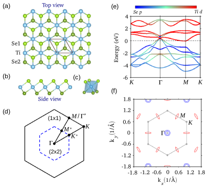
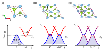
The TiSe2 monolayer has an hexagonal Bravais lattice with the space group () TiSe2M_CDWSTM ; TiSe2M_CDWNC . It consists of three sublayers stacked in the order Se-Ti-Se within a single unit cell, as shown in Figs. 1(a)-1(c). The two Se sublayers are strongly bonded with the Ti plane in the middle (bond length 2.56 Å) and Ti has an octahedral prismatic coordination as illustrated in Fig. 1(c). The first BZ is hexagonal with three high symmetry points , , and , as shown in Fig. 1(d). This BZ can be obtained by projecting the 3D bulk BZ onto the (001) surface and, therefore, the points corresponding to the CDW wavevector in the bulk ( and in the 3D BZ) map into points of the 2D BZ. The PLD doubles the original lattice periodicity forming a superstructure and, hence, reduces the 2D BZ, which is shown by broken blue lines in Fig. 1(d). Due to the BZ folding, the original points of the BZ are mapped into the zone center () of the BZ.
Beginning with a monolayer in the normal phase, a simplistic ionic insulator model suggests a strong tendency for electron transfer from the Ti and orbitals to the states of Se. Valence and conduction bands would then arise from Se and Ti states, respectively. However, in reality, the crystalline environment and spatial extent of the orbitals increase their bandwidth such that conduction and valence bands overlap. Figure 1(e) shows that, near the Fermi level, the Se -derived valence bands are centered at the -point whereas the Ti -derived conduction bands lie at the -point. These overlap in energy and make TiSe2 a semimetal in the normal phase. The Fermi contours reveal a pair of hole pockets at the -point whereas a single elongated elliptical electron pocket forms at the -point, as shown in Fig. 1(f). In order to equivalently quantify a band overlap or band gap, we define the indirect gap as the difference between the minimum of the conduction band at the -point and the maximum of the valence band at . A negative value of the gap therefore represents a semimetal with indirect band overlap, while an insulator will have a positive gap. We find an indirect band gap of eV using GGA, and a smaller value of eV with an HSE functional. Although these values are different from some experimentally reported values of 0.098 eV TiSe2M_CDWNC ; TiSe2M_CDWNano , they agree well with earlier bandstructure calculations TiSe2M_CDWNC . The difference with respect to the experimental data may arise because our DFT calculations assume K whereas the normal structure, in reality, exists only at higher temperatures.
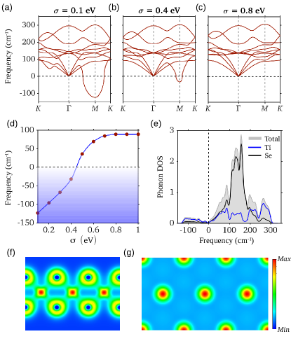
The phonon dispersion of the normal phase is shown in Fig. 2 for different values of the electronic smearing parameter using a Methfessel-Paxton smearing Sm_MethPax . This parameter determines the smearing width and is normally used as a technical tool to accelerate convergence in DFT calculations. However, when used with the Fermi-Dirac distribution, it mimics the electronic temperature and thus describes the occupation probability of the electronic states TiSe2B_ThSm ; Sm_FD ; Sm_MethPax . By varying , we can qualitatively estimate changes expected to occur in the phonon spectrum with increasing temperature, thereby monitoring the structural stability at different temperatures. In Fig. 2(a) we show the phonon spectrum at a small smearing parameter. It is clear that the system is dynamically unstable with a Kohn-type kohn_anoM soft mode at the -point. The partial phonon density of states is shown in Fig. 2(e) and demonstrates the imaginary frequencies are inherent to the Ti atoms, suggesting that the CDW is associated with the Ti sublayers. The structural instability at the -point is consistent with the commensurate PLD observed in experiments at low temperature. As we increase , the range over which the soft mode has imaginary frequency is reduced, and finally disappears for eV [see Fig. 2(a)-2(d)]. This dependence of the soft mode frequency on indicates a structural phase transition with temperature and confirms that the structure is stable only above a threshold temperature footnote1 ; footnote2 .
Phonons and electrons are inseparably intertwined in a crystal which prevents, in principle, the simplistic assignment of the CDW/PLD tendency to an instability of the electronic or phonon subsystems (through electron-phonon coupling), independently. In a simplistic description of this “hierarchy”, a transition driven entirely by electronic interactions, the PLD would be regarded “secondary”, as a readjustment of the ions to a modified Born-Oppenheimer potential TMDC_CDWReview ; FermiSurfNest ; TiSe2B_ThMech , or it might not even occur at all, as seems to be the case, for example, in the layered purple bronze K0.9Mo6O17 Mou2016 ; Su2016 . The non-uniform charge density would therefore emerge regardless of whether or not the ions are clamped at their high symmetry positions FermiSurfNest ; TiSe2B_ThMech . Figures 2(f)-2(g) show the charge density distribution in various crystal planes in an undistorted superstructure of TiSe2 monolayer. They show no appreciable charge redistribution in the presence of a doubled lattice periodicity, similarly to the previously studied case of the bulk material TiSe2B_ThMech . This, however, must be interpreted with care, as a consistency check, and not as confirmation that the role of electronic interactions is secondary. Such conclusion would be rather primitive because, on the one hand, systems where CDW arise only from electronic interactions are usually strongly correlated and, on the other, the GGA XC functional cannot capture correlations at that level. In fact, in bulk TiSe2, the inclusion of many-body corrections at the level of the approximation has been shown to capture the spectral reconstruction and gapped state seen experimentally even without any deformation (i.e. in a cell calculation) Cazzaniga2012 , which underscores that electronic correlations are indeed of crucial importance to describe the electronic state through the CDW transition. The charge distributions seen in Fig. 2(g)] are spherically symmetric near the Ti atoms and nearly constant in the interstitial region. This is a reminiscent feature of the metallic-type ionic environment and suggests that Ti atoms are more likely to displace in their hexagonal plane to find an energy minimum.
III The distorted phase
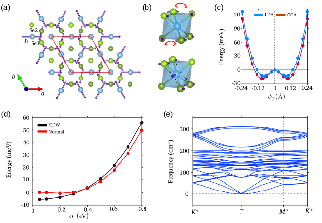
We now investigate the superstructure to find the equilibrium configuration in the distorted phase. We have allowed all the ions’ positions to relax using both the LDA and GGA functionals. Figures 3(a)-3(b) illustrate the atomic movement in the fully relaxed superstructure. Both the GGA and LDA predict the CDW instability, with an energy reduction of 4.7 meV and 3.7 meV per chemical unit, respectively. Interestingly, despite unconstrained, our results show that all atoms move only in their respective atomic planes without any out-of-plane distortion. The in-plane atomic displacements give rise to two different local octahedral structures in the superstructure: in one octahedron, Ti atoms remain the center of the coordination unit while top (bottom) Se atoms are displaced clockwise (counterclockwise) in a circular fashion without affecting the original Ti-Se bond length, as depicted in the Figure. In contrast, Ti atoms in the second octahedron are displaced off-center giving rise to a distorted octahedron with three different Ti-Se bond lengths, as shown in the lower part of Fig. 3(b). Even though our calculations with either the GGA or LDA functional yield similar atomic displacement patterns, the magnitude of the atomic displacements depends strongly on the functional used. The calculated atomic displacements () for Ti (Se) are 0.090 (0.029) Å and 0.076 (0.016) Å with the GGA and LDA functional, respectively. The atomic displacement ratio with the GGA functional is , which agrees well with experiments TiSe2B_expN ; TiSe2M_CDWNC .
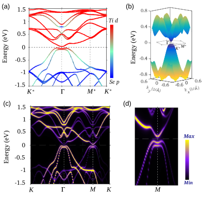
Fig. 3(d) presents a complementary analysis of the relative stability of the distorted and undistorted configurations in terms of the energies per chemical unit of each phase obtained for different smearing parameters . The distorted phase has lower energy than the normal phase for small , and is thus more stable at lower temperature. As we increase , the energy of the distorted phase increases and surpasses that of the normal phase at eV. This behavior is in accord with the normal phase phonon analysis presented above [cf. Fig. 2] and further confirms the stability of the normal phase structure above a threshold temperature.
The phonon spectrum of the fully relaxed superstructure is shown in Fig. 3(e). The absence of imaginary frequencies in the whole 2D BZ reflects the dynamical stability of this configuration at K, and indicates that it is the ground state structure of the TiSe2 monolayer. This is further supported by the local energy landscape of the CDW phase that we analyzed by changing the atomic distortion manually and computing the changes in total energy; the results are shown in Fig. 4(c). It should be noted that the Se atoms were fully relaxed for each manually set . The energy is minimal at a finite value of (in the plane), and a spatial reversal of the distortion yields a degenerate configuration. The system can then freeze in either configuration at low temperature. At higher temperature, however, thermal effects allow the system to fluctuate between configurations giving rise to an “average” structure characteristic of the normal state.
Figure 4(a) displays the electronic band structure of the relaxed superlattice, and shows the emergence of a full band gap in the BZ [see Fig. 4(b)] at the Fermi level. The orbital character of the Bloch states is represented by the color map superimposed on each curve. It is clear that the coupling between the predominantly Ti-derived conduction band orbitals at and the predominantly Se-derived valence orbitals at lifts the band overlap that is present in the normal state and lowers (raises) the energy of the filled (empty) states in the vicinity of that becomes gapped.
In order to facilitate direct comparison with experimental dispersions TiSe2M_CDWNC ; TiSe2M_CDWNano , in Figs. 4(c)-4(d) we unfolded the superlattice band structure to the original BZ. The most significant feature in this representation is the clear presence of back-folded bands at the -point which, despite their smaller spectral weight, provide a prominent signature of the new periodic potential in the CDW phase. The CDW phase in TiSe2 has been recently investigated experimentally by ARPES, whose spectra reveal the formation of a superlattice with a band gap of 153 meV at 10 K and two back-folded bands at the -point TiSe2M_CDWNC ; TiSe2M_CDWNano . The spectral weight of the back-folded bands at the M-point is smaller than that of the bands at TiSe2M_CDWNC . These experimental results are well captured by our first-principles results. The insulating electronic state with a band gap of 82 meV (325 meV) with GGA (HSE) and the location and intensity of the two back-folded bands at the -point are in reasonable agreement with those experiments.
Finally, we highlight the fact that, in addition to obtaining magnitudes of the lattice distortion and electronic gap which are accurate in comparison with experiments, we obtain also the non-trivial restructuring of the bands around that has been analyzed in detail on the basis of ARPES spectra in bulk TiSe2 TiSe2B_expARPES_EHC ; TiSe2B_exp_Exct . This is best seen in the close-up of Fig. 4(d) that shows the lowest conduction band around remaining parabolic, whereas the valence band acquires a Mexican-hat type dispersion. Combined with finite temperature broadening, the latter causes a flattening of the top of the valence band, an effect that has been seen clearly by ARPES in bulk samples TiSe2B_expARPES_EHC ; TiSe2B_exp_Exct . The qualitative significance of this reconstruction within a DFT calculation was first highlighted by Cazzaniga et al. in studies of the distorted phase in the bulk Cazzaniga2012 . In that case, corrections on top of the LDA are seen to capture the experimental Mexican-hat reconstruction even in an undistorted cell. It is very interesting that, contrary to the bulk case, the monolayer shows this reconstruction already at the GGA level, Fig. 4(c), without needing to add many-body corrections beyond the XC functional. As argued in detail in Ref. Cazzaniga2012 , this fact strongly supports the built-in tendency of this electronic system towards an excitonic-insulator state, which predicts precisely such type of spectral reconstruction Kohn_EI . It is noteworthy that such physics is captured already at the GGA level in the monolayer which, providing a more rudimentary account of the electronic interactions than the approximation, perhaps suggests a stronger tendency for the excitonic instability in the monolayer in comparison with its bulk counterpart.
IV Discussion and concluding remarks
The results presented above provide a careful and comprehensive analysis of the stability of a TiSe2 monolayer, and establish the PLD as the stable structure in the ground state. Fig. 5 provides a schematic distillation of the essential physics following from our calculations. Fermi surface nesting is certainly excluded as the cause of this PLD/CDW instability because of the ill defined nesting of the circular/elliptical Fermi surfaces seen both in our results and in experiments FermiSurfNest ; TiSe2M_CDWNano ; TiSe2M_CDWNC . The absence of any charge density redistribution in a clamped ion superlattice [cf. Figs. 2(f) and 2(g)] indicates that the CDW and PLD are intimately related in the monolayer, similarly to the bulk. It is then clear that the electron-phonon coupling is significant in this system because of the large lattice distortions it attains in comparison with similar CDW-prone TMDs TiSe2B_Th ; TMDC_CDWReview .
Even though the problem is unavoidably interacting and self-consistent, there is a long standing interest in establishing to which extent the CDW is driven here primarily by an electronic instability, or by a strong electron-phonon coupling with negligible influence of electronic correlations (as happens, for example, in metallic TMDs such as NbSe2 Zhu_CDW ). This is especially important to formulate analytical microscopic models capable of describing the CDW and superconductivity seen in TiSe2 as a function of electron doping, because the presence of strong electronic interactions can affect the pairing instability both quantitative and qualitatively.
It is generally difficult to answer this question from a purely DFT perspective and much less quantify precisely the role of electron-electron interactions because of their approximate treatment in any practical implementation. Nevertheless, combined with the experience and evidence learned from earlier studies of bulk TiSe2, the present results reinforce the view that interactions play a rather consequential role here. One line of evidence arises from the fact highlighted earlier that our calculated distortions and restructured band dispersions in this phase are in good agreement with experimental results, but these properties are seen to quantitatively and strongly depend on the type of XC approximation used as mentioned earlier. Similar considerations apply to the stability of the PLD phase at which is not reproduced at the LDA level, for example Olevano2014 . Since our calculations rely on fully relaxed ions and explicitly converged -sampling, we are confident that this variation reflects directly the different treatment of interaction effects in those implementations of the XC functional. The other line of evidence is related to the spectral reconstruction in the distorted phase, and the reproduction within the GGA of the Mexican hat profile characteristic of the ARPES quasiparticle spectra. Such bandstructure is expected as the self-consistent ground state in the excitonic-insulator scenario, and can be obtained from a mean-field type analysis of the Coulomb interactions between holes at and electrons at based on effective non-interacting bands for the reference (normal) state Kohn_EI ; Money:2009 ; Wezel:2010 . The reproduction of this at the DFT level is a non-trivial outcome and, in fact, previously seen only in the electronic structure of bulk TiSe2 after the inclusion of many-body corrections Cazzaniga2012 (and apparently in no other electronic system to date). That the monolayer shows such spectral reconstruction without many-body corrections to the GGA bolsters the view that excitonic correlations do play a key role in the CDW transition.
This study underlines that these monolayers are an exciting material platform to study CDW phases in general, have an interesting phase diagram on their own, and will contribute to illuminate the dominant and long-sought mechanism responsible for the CDW instability, both in bulk and monolayer TiSe2.
acknowledgments
The work at the National University of Singapore was supported by the Singapore National Research Foundation under the NRF fellowship Award No. NRF-NRFF2013-03 (HL), by the Singapore Ministry of Education Academic Research Fund Tier 2 under Grant No. MOE2015-T2-2-059 (VMP), and benefited from the HPC facilities of the NUS Centre for Advanced 2D Materials. WFT is supported by the National Thousand-Young-Talents Program, China.
References
- (1) K. S. Novoselov et al., Proc. Natl. Acad. Sci. USA 102, 10451 (2005).
- (2) S. Z. Butler et al., ACS Nano 7, 2898 (2013).
- (3) K. S. Novoselov, A. Mishchenko, A. Carvalho, and A. H. Castro Neto, Science 353, aac9439 (2016).
- (4) H. Terrones, F. Lopez-Urias, and M. Terrones, Sci. Rep. 3, 1549 (2013).
- (5) K. F. Mak, C. Lee, J. Hone, J. Shan, and T. F. Heinz, Phys. Rev. Lett. 105, 136805 (2010).
- (6) Y. Zhang et al., Nat. Nanotechnol. 9, 111 (2014).
- (7) K. Rossnagel, J. Phys.: Cond. Mat. 23, 213001 (2011).
- (8) Y. Yu et al., Nat. Nanotechnol. 10, 270 (2015).
- (9) J.-A. Yan, M. A. D. Cruz, B. Cook, and K. Varga, Sci. Rep. 5, 16646 (2015).
- (10) M. D. Johannes and I. I. Mazin, Phys. Rev. B 77, 165135 (2008).
- (11) L. J. Li et al., Nature 529, 185 (2016).
- (12) R. Ganesh, G. Baskaran, J. van den Brink, and D. V. Efremov, Phys. Rev. Lett. 113, 177001 (2014).
- (13) Q. H. Wang, K. Kalantar-Zadeh, A. Kis, J. N. Coleman, and M. S. Strano, Nat. Nanotechnol. 7, 699 (2012).
- (14) D. Xiao, G.-B. Liu, W. Feng, X. Xu, and W. Yao, Phys. Rev. Lett. 108, 196802 (2012).
- (15) N. R. Pradhan et al., ACS Nano 8, 7923 (2014).
- (16) F. J. Di Salvo, D. E. Moncton, and J. V. Waszczak, Phys. Rev. B 14, 4321 (1976).
- (17) R. Z. Bachrach, M. Skibowski, and F. C. Brown, Phys. Rev. Lett. 37, 40 (1976).
- (18) T. E. Kidd, T. Miller, M. Y. Chou, and T.-C. Chiang, Phys. Rev. Lett. 88, 226402 (2002).
- (19) K. Rossnagel, L. Kipp, and M. Skibowski, Phys. Rev. B 65, 235101 (2002).
- (20) J. von Boehm, H. Isomäki, and P. Krusius, Physica Scripta 22, 523 (1980).
- (21) D. L. Duong, M. Burghard, and J. C. Schön, Phys. Rev. B 92, 245131 (2015).
- (22) R. Bianco, M. Calandra, and F. Mauri, Phys. Rev. B 92, 094107 (2015).
- (23) V. Olevano et al., Phys. Rev. Lett. 112, 049701 (2014).
- (24) Z. Zhu, Y. Cheng, and U. Schwingenschlögl, Phys. Rev. B 85, 245133 (2012).
- (25) M. Cazzaniga et al., Phys. Rev. B. 85, 195111 (2012).
- (26) H. Cercellier et al., Phys. Rev. Lett. 99, 146403 (2007).
- (27) E. Morosan et al., Nat. Phys. 2, 544 (2006).
- (28) A. F. Kusmartseva, B. Sipos, H. Berger, L. Forró, and E. Tutiš, Phys. Rev. Lett. 103, 236401 (2009).
- (29) P. Goli, J. Khan, D. Wickramaratne, R. K. Lake, and A. A. Balandin, Nano Lett. 12, 5941 (2012).
- (30) J.-P. Peng et al., Phys. Rev. B 91, 121113 (2015).
- (31) P. Chen et al., Nat Commun 6, 8943 (2015).
- (32) K. Sugawara et al., ACS Nano 10, 1341 (2016).
- (33) G. Kresse and J. Furthmüller, Phys. Rev. B 54, 11169 (1996).
- (34) G. Kresse and D. Joubert, Phys. Rev. B 59, 1758 (1999).
- (35) P. Hohenberg and W. Kohn, Phys. Rev. 136, B864 (1964).
- (36) J. P. Perdew, K. Burke, and M. Ernzerhof, Phys. Rev. Lett. 77, 3865 (1996).
- (37) S. Baroni, P. Giannozzi, and A. Testa, Phys. Rev. Lett. 58, 1861 (1987).
- (38) A. Togo, F. Oba, and I. Tanaka, Phys. Rev. B 78, 134106 (2008).
- (39) N. D. Mermin, Phys. Rev. 137, A1441 (1965).
- (40) P. E. Blöchl, O. Jepsen and O. K. Andersen, Phys. Rev. B 49, 16223 (1994).
- (41) M. Methfessel and A. T. Paxton, Phys. Rev. B 40, 3616 (1989).
- (42) V. Popescu and A. Zunger, Phys. Rev. B 85, 085201 (2012).
- (43) W. Ku, T. Berlijn, and C.-C. Lee, Phys. Rev. Lett. 104, 216401 (2010).
- (44) P. V. C Medeiros, S. Stafström, and J. Björk, Phys. Rev. B 89, 041407(R) (2014).
- (45) P. V. C Medeiros, S. S. Tsirkin, S. Stafström, and J. Björk, Phys. Rev. B 91, 041116(R) (2015).
- (46) W. Kohn, Phys. Rev. Lett. 2, 393 (1959).
- (47) Our calculated critical smearing parameter strongly depends on the smearing method used in calculations, consistent with Ref. TiSe2B_ThSm . It should be noted that while can be used to access qualitative changes in the phonon spectrum and stability with temperature, its direct relation with the temperature relies on the smearing function used vasp ; Sm_FD ; Sm_MethPax ; Sm_gauss .
- (48) Note that the phonon spectrum is calculated within the harmonic approximation whereas an estimation of the exact transition temperature () explicitly needs to consider quasi-harmonic effects phonopy . The dependence only changes the filling of energy bands without inducing noticeable structural changes TiSe2B_ThSm . It will be interesting to estimate in the future through either calculating volume dependence of phonon spectrum phonopy or using finite-difference phonon results with large displacements qha_Antolin ; qha_lazar .
- (49) D. Mou et al., Phys. Rev. Lett. 116, 196401 (2016).
- (50) L. Su, C.-H. Hsu, H. Lin, and Vitor M. Pereira, Phys. Rev. Lett. 118, 257601 (2017).
- (51) N. Antolin, O. D. Restrepo, and W. Windl, Phys. Rev. B 86, 054119 (2012).
- (52) P. Lazar, J. Martincová, and M. Otyepka, Phys. Rev. B 92, 224104 (2015).
- (53) D. Jérome, T. M. Rice, and W. Kohn, Phys. Rev. 158, 462 (1967).
- (54) X. Zhu et al., Proc. Natl. Acad. Sci. USA 112, 2367 (2015).
- (55) J. van Wezel, P. Nahai-Williamson, S. S. Saxena, Phys. Rev. B. 81, 165109 (2010).
- (56) C. Monney, H. Cercellier, F. Clerc, C. Battaglia, E. F. Schwier, C. Didiot, M. G. Garnier, H. Beck, P. Aebi, H. Berger, L. Forro, and L. Patthey, Phys. Rev. B. 79, 45116 (2009).