Electrical Transport Properties of Polycrystalline and Amorphous TiO2 Single Nanotubes
Abstract
The electrical transport properties of anodically grown TiO2 nanotubes was investigated. Amorphous nanotubes were anodically grown on titanium foil and transformed through annealing into the anatase phase. Amorphous and polycrystalline single nanotubes were isolated and contacted for measurements of the electrical resistance. Non-linear current-voltage characteristics were explained using the fluctuation induced tunneling conduction model. A clear enhancement of the conductance was induced in an insulating anatase nanotube through low-energy Ar/H ion irradiation. Confocal Raman spectroscopy shows that the annealed samples were in anatase phase and a blueshift due to phonon confinement was observed.
pacs:
73.63.Fg,78.30.FsI Introduction
Titanium dioxide nanotube arrays, formed by self-organizing anodization, have attracted considerable attention. These 1D structures are used in wide range of applications such as electrodes in catalysis Hadjiivanov and Klissurski (1996), photocatalysis Fujishima and Honda (1972), dye-synthesized solar cells O’Regan and Grätzel (1991), gas sensors Seo et al. (2009), photoelectrochemical water splitting Momeni and Ghayeb (2015a, b), in batteries Aricó et al. (2005) or for CO2 reduction Woolerton et al. (2010); Varghese et al. (2009). Biocompatible Ti46Si12O42 nanostructured surfaces can be used to enhance cell attachment and proliferation Zhao et al. (2016). This outstanding flexibility is a consequence of different electronic, chemical and ionic properties of anatase, brookite and rutile Diebold (2003); Chen and Mao (2007). Anatase is often more interesting for applications, such as solar cells, due to the larger electron mobility compared to rutile. Tang et al. (1994) The combination with the large active surface area of nanostructures, results in a variety of dielectric, conducting, magnetic, catalytic and other physical and chemical properties. Doping can be used to enhance the photo catalytic activity of TiO2 nanotubes, e.g. with W Momeni et al. (2017); Momeni and Ghayeb (2016a); Momeni et al. (2015a), Au/W Momeni and Ghayeb (2016b), Co Momeni et al. (2015b); Momeni and Ahadzadeh (2016), or Co Momeni and Ghayeb (2016a).
The general mechanism of electron transport, particularly in nanostructures of TiO2 , is not well studied and understood. Most of the published work focuses on macroscopic samples such as nanotubular arrays Mor et al. (2006); Lai et al. (2005), where parasite effects such as contact contributions in two-point (2P) measurements or the scattering of light inside the tangle of tubes, can have considerable influence on the measurements. Depending on the contacts, non-metallic clusters (Au), Schottky barriers (Pt) or oxide layers (Al, Cr) could be formed Diebold (2003). The magnetic Choudhury and Choudhury (2013); Stiller et al. (2016) and electrical transport properties of TiO2 depend strongly on structural defects (single crystal band gap: eV Sanjines et al. (1994); Pascual et al. (1978)), such as oxygen or titanium vacancies. The transport properties can also be strongly influenced by the scattering on the sample surface, as was found for polycrystalline macroscopic arrays of TiO2 nanotubes Muñoz (2007). In addition, it was shown that, intragrain and intergrain conduction processes play an important role in disordered nanowires and nanotubes Stiller et al. (2015); Sattler (2011). Therefore, a large number of different resistivities have been reported, e.g. cm (2P, top/bottom tube contacts) Tighineanu et al. (2010), cm Stiller et al. (2013) and cm Fàbrega et al. (2010) using a four-point (4P) probes method. For comparison, the obtained resistivity of different polycrystalline bulk anatase covers a large range: cm Tang et al. (1994); Akl et al. (2006); Huber et al. (2004).
Recently, fluctuation induced tunneling conductance (FITC) Sheng (1980) has been proposed as a responsible mechanism in ZnO nanowires Stiller et al. (2015), in bundles of double-walled carbon nanotubes Barzola-Quiquia et al. (2015) and in nanoporous TiO2 thin films Konezny et al. (2011). The FITC model predicts non-linear current-voltage curves due to intrinsic barriers between grains in the sample Sheng (1980). Other frequently used mechanisms include variable-range hopping and thermally activated processes. However, they cannot explain the non-linear behavior of curves Stiller et al. (2015) and the saturation of the resistivity at low temperature Hassan et al. (2003); Barborinia et al. (2005).
In this work, procedures to isolate single TiO2 nanotubes and to establish barrier free contacts for electrical transport measurements are presented. The resistance of amorphous and polycrystalline anatase samples were investigated in a broad temperature range. A FITC mechanism contributes to the conductivity in all measured samples with non-linear curves. Additionally, the electrical transport of a highly insulating anatase nanotube was modified by means of defect production at the surface using low-energy ion irradiation.
II Experimental
The TiO2 nanotubes have been separated from nanotubular layers anodically grown on titanium foil (Advent Research Materials Ltd., 99.6 % purity) in an electrochemical cell with ethylene glycol electrolyte containing 0.15 M ammonium fluoride and 1 M H2O. The titanium foil was anodized with a potential of 60 V applied for 5 hours. Finally, the nanotubular array was placed in ethanol and dried with nitrogen gas.
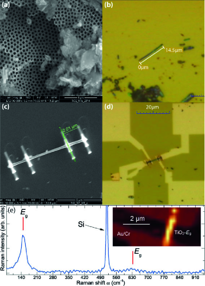
The grown nanotubes (see Figure 1(a)) are initially in the amorphous phase and were annealed in air using a Rapid Thermal Annealer (Jet-first Rapid Thermal Annealer, Jipilec, France) in order to obtain polycrystalline anatase samples. The heating/cooling rate was 15°∘Cmin with annealing temperatures of 350∘C and 450∘C. After annealing, the nanotubes were polycrystalline and exhibited anatase morphology, for more detailed information please refer to Refs. Albu et al. (2010); Lee et al. (2014); Soa et al. (2016). Annealing at higher temperatures results in mixed phases of anatase and rutile, eventually, the single nanotubes would collapse Lee et al. (2014). Therefore, only pure amorphous and anatase nanotubes were investigated.
Bundles of nanotubes were scratched off the foil onto commercial, p-boron doped silicon substrates ( mm) with a 150 nm SiNx coating, see Figure 1(b). By applying pressure and a slow circular motion using a second substrate, some single nanotubes break off the bundles and were stuck to the substrates because of electrostatic attraction. Suitable tubes were selected using an optical microscope. In order to fix the nanotubes on the substrate and to prepare them for contacting, electron beam induced deposition (EBID) of tungsten carbide was used, see Figure 1(c). The deposited WCx is nearly insulating Spoddig et al. (2007) and provides the necessary steps to compensate the height difference between contacts and nanotube. The substrates were covered with a positive working resist (ALL-RESIST, PMMA 950 K, AP-R 671-05) and, by means of electron beam lithography (EBL), the structures of the contacts were printed into the resist. After developing, a bilayer film composed of Cr (5 nm) and Au (35 nm) was sputtered. The PMMA was later removed by acetone. The width of the contacts exceeds the WCx steps, in order to get a potential barrier-free electrical connection. A prepared nanotube can be seen in Figure 1(d). An overview of the structural properties and dimensions of the nanotubes can be seen in Table 1.
| ID | Phase | Contacts | Length (m) | |
|---|---|---|---|---|
| NT1 | Anatase | 4 | 0.026 | |
| NT2 | Anatase | 4 | 0.044 | |
| NT3 | Amorph | 2 | 5.31 | |
| NT4 | Anatase | 2 | 34 |
For the transport measurements, each sample was contacted on a chip carrier placed on the cold head of a standard closed cycle cooling system inside a vacuum bell with a minimum temperature of K. The electrical resistance was measured using the four-point probe configuration with a current source (Keithley 6221) and a nano- voltmeter (Keithley 2182). The high resistance measurements were performed with a constant applied voltage using a DC source (Yokogawa 7651). The current was monitored with a shunt resistance of in series with the samples. For low temperature measurements down to K, a commercial 4He cryostat (Oxford Instruments) was used.
The Ar ion irradiation was done in a self-made plasma chamber with a parallel plate (copper) setup at room temperature. The chamber was evacuated to a pressure of mbar with an Ar/H gas mixture (Ar: 90 % and H: 10 %, Air Liquide) flowing through the chamber. The chip carriers with samples were mounted cm away from the plasma center and a bias voltage of V was used to accelerate the ions towards the sample, while connected to ground, and the bias current was measured. The energy used is too low to produce any relevant sputtering, which could induce a composition variation. Previously, the substrate was covered with PMMA and a window was opened to shield the contacts using electron beam lithography. The number of ions hitting the sample was estimated to be Ar ions Stiller et al. (2016).
Information about the sample structure was obtained using the confocal Raman microscope alpha300R+ from WITec with an incident laser light of wavelength nm. The device has a lateral resolution of nm and a depth resolution of nm. The energy was kept at mW to avoid damage caused by heating effects in the sample.
III Results
Using XRD, it was shown that the as-prepared nanotube bundles are amorphous and they transform into anatase after annealing Albu et al. (2010); Lee et al. (2014). However, some single nanotubes could remain in the amorphous state. Using confocal Raman spectroscopy, single isolated samples can be investigated. According to Ohsaka et al. Ohsaka et al. (1978) for bulk anatase, Raman peaks can be found at 639 cm-1, 197 cm-1 and 144 cm-1, assigned as modes. modes are at 513 cm-1 and 399 cm-1, and the band at 519 cm-1 corresponds to the mode. The Raman band at 144 cm-1 is the most intense peak. Our results are presented in Figure 1(e), the peaks correspond to the band, the obtained values are 148 cm-1 and 633 cm-1, respectively, which are different compared to the above mentioned results for the bulk anatase. This band shift is known as blueshift and is caused due to phonon confinement in the nanocrystals forming the nanotube. This effect was already reported for anatase nanocrystals Zhang et al. (2000), where the shift of the peak as a function of the annealing temperature was investigated. A blueshift to 148 cm-1 was obtained for nanocrystals annealed at C, which is in agreement with the annealing temperature used for the TiO2 nanotube. From the blueshift, a crystallite size of nm could be obtained Zhang et al. (2000), which is in agreement with XRD results Lee et al. (2014). A Raman scan is shown in the inset of Figure 1(e), where the bright shades correspond to the Raman band at 148 cm-1.
The electrical properties of the nanotubes depend strongly upon the phase and structural quality. A defect free TiO2 anatase nanotubes is electrical insulating. However, due to growth conditions, defects can be introduced resulting in an electrical conductive material. For example, such defects are oxygen vacancies (self doping) produced by a reduction of TiO2, e.g. through electrochemical reactions, gas annealing or exposure to vacuum Lee et al. (2014); Liu et al. (2014); Paramasivam et al. (2012); Ghicov et al. (2006), due to a separation of O2 or H2O from terminal oxide or hydroxide groups and bridged oxide and Ti3+ states Paramasivam et al. (2012). Many investigated nanowires andor nanotubes exhibit non-linear curves, which are usually neither discussed, nor explained in the literature Chiu et al. (2009). Such non-ohmic behavior could be due to intergrain conduction or barriers formed on the contacts used for measurements. For convenience, the measured samples in this work are sorted in three categories: polycrystalline nanotubes with linear (Section III.1) and non-linear (Section III.2) curves, an amorphous sample (Section III.3) and an insulating anatase nanotube which was treated with low-energy Ar ions (Section III.4).
III.1 Linear curves
The TiO2 nanotube sample NT1 shows linear curves in the whole investigated temperature range, see inset in Figure 2. Similar results were already shown in previous work Stiller et al. (2013). The measurements were carried out using the four-point probes method. The temperature dependence of the resistance can be seen in Figure 2, which
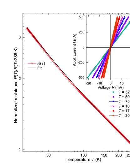
can be fitted using the Mott variable range hopping (VRH) model Stiller et al. (2013):
| (1) |
where is an arbitrary prefactor, is a temperature independent term, the dimensionality and is a characteristic temperature. From the fit, K; similar values have already been reported in the literature Stiller et al. (2013). The density of states (DOS) at the Fermi level can then be calculated:
| (2) |
where is Boltzmann constant and the localization length is assumed to be in the order of nm Chen et al. (1997). A DOS of was found, which agrees very well with the literature Stiller et al. (2013); Yildiz et al. (2007). The resistivity, see Table 1, is very low compared to other investigated samples. The low resistivity might be a consequence of doping due to a large density of defects present in the sample.
III.2 Non-linear curves
The current-voltage characteristics using Mott VRH and activated transport processes correspond to linear curves (ohmic regime).Therefore, they fail to explain non-linear curves as well as for such samples. The conduction of the polycrystalline nanotube depends on the intragrain and intergrain conductivity. When there is no doping, the grains are insulating with an energy gap of eV. At intermediate doping, the charge carriers move to the crystal defects/boundaries between the grains, which are acting as electronic traps, and thus a depletion layer is formed with a potential barrier. In this case non-linear curves can be observed also when measuring with four-point probes method. At high doping levels, the material is saturated and the barrier vanishes again.
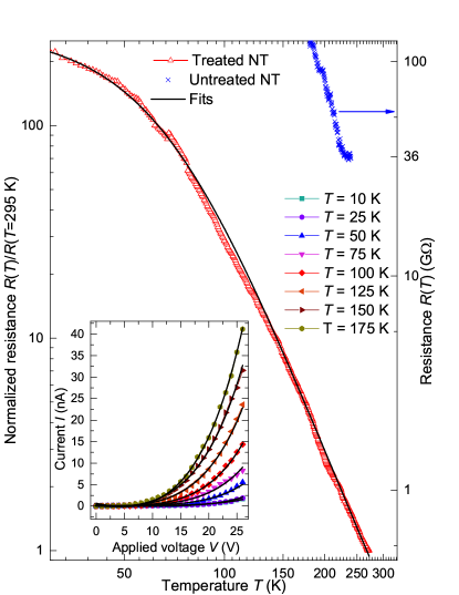
The nanotube NT2 was measured using four contacts and shows non-linear curves, see inset Figure 3.
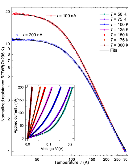
The measurements were performed from K to K, where non-linear behavior can be observed at temperatures K and below. This can also be seen in the temperature dependent resistance measurements, which were done using nA and nA, at K the curves split. The non-linearity of the curves and the temperature dependence can be explained using the fluctuation induced tunneling conductance (FITC) model, which was already used to describe similar materials such as nanoporous TiO2 thin films Konezny et al. (2011), ZnO nanowires Stiller et al. (2015), oxide nanostructures Filipi et al. (2007); Lin et al. (2008); Lin and Lin (2011), double walled carbon nanotube bundles Barzola-Quiquia et al. (2015) or disordered semiconductors Redfield (1975). According to the FITC model, at small applied electric fields, the temperature dependent resistance across a junction is given by Sheng (1980)
| (3) |
where is a free, temperature independent parameter, and the characteristic temperatures are defined as
| (4) | ||||
where is the vacuum permittivity, the dielectric constant of the barrier, the elementary charge, is the Boltzmann constant, the reduced Planck constant, the electron mass, the area of the tunnel junction, the barrier height and is the barrier width. The characteristic energy can be regarded as the energy required for an electron to pass the barrier and is the temperature for which well below thermal fluctuations become insignificant. As stated before, the FITC model also provides the means to describe the non-linear curves at different temperatures as follows Sheng (1980):
| (5) |
where and are the saturation current and critical voltage, respectively, and is given as:
| (6) |
As can be seen from these equations, the characteristic temperatures can be obtained through fitting the curves and the temperature dependent resistance . However, in order to fit the data, a temperature independent term in parallel to the FITC conduction process, has to be added. The parallel contribution is due to disorder and impurities present in the TiO2 nanotubes.
In order to fit the data and to reduce the amount of free parameters, all curves were fitted simultaneously ( curves and ) and the corresponding parameters were taken as shared parameters for all curves. This means, that and (which depend only weakly on the temperature) are shared among the data of the curves, and that and are shared among the curves and results. The data and the fits can be seen in Figure 3, the FITC model describes very well both the curves and results. From the fit results, a saturation current of A and a critical voltage of V are obtained. The characteristic temperatures are K and K. Similar values have already been reported in the literature Lin et al. (2008); Lin and Lin (2011); Xie and Sheng (2009); Stiller et al. (2015). Although, the samples were measured using the four-point probes method, non-linear curves were measured as consequence of barriers formed at the intergrain boundaries. This effect could be avoided by employing long term annealing at intermediate temperatures, as high-temperature annealing would result in a collapse of the TiO2 nanotubes Lee et al. (2014); Albu et al. (2008); Mohammadpour et al. (2016); Soa et al. (2016).
III.3 Amorphous nanotube
The temperature dependent resistance of an amorphous TiO2 nanotube NT3 is shown in Figure 4.
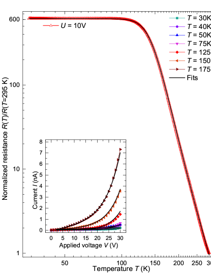
The room temperature resistance is , and thus much higher than the previously shown samples. Therefore, the resistance was measured with a constant applied voltage of V and the current was monitored with a shunt resistance. This implies a two point-probes technique to be used. However, a large influence of the contacts is not expected, due to the very high resistance of the TiO2 nanotube itself. This assumption is supported by the result of a four-point probes measurement at room temperature, which yields the same resistance as for the two-point measurement. Therefore, the influence of the contacts will be neglected. The data as well as the fits are shown in Figure 4, in the inset the curves can be seen. As before, all measurements were fitted simultaneously. In order to fit the data, not only the FITC model has to be assumed but also a VRH hopping contribution in parallel was needed, see Eq. (1). The shared parameters were: A, V, and K. With the characteristic temperature K and using Eq. (2), the DOS at is eV-1m-3. This value is one order of magnitude smaller than what was obtained for TiO2 nanotube with linear curves. This together with the large values of and , i.e. large barrier height, explain the high resistance of this sample. At low temperature, the constant term in parallel which is due to impuritiesdefects, dominates the transport.
III.4 Ar ion irradiated nanotube
In order to investigate the influence of defects on the transport properties of polycrystalline anatase TiO2 nanotubes, an almost insulating sample was chosen (see results in Figure 5), indicating a high quality of the crystalline structure. The sample NT4 has been irradiated using an Ar/H plasma. The results after irradiation of the temperature dependent resistance measurements and curves can be seen in Figure 5 and its inset.
The used energy of the plasma ions of V and, according to SRIM simulations, the resulting penetration depth is nm, implying that the nanotube is modified only at the surface Stiller et al. (2016, 2015). The sample consists then of an insulating polycrystalline nanotube surrounded by a conducting TiO2 shell. The FITC model is suitable to describe such systems, which is in agreement with the non-linear curves. Although the sample was irradiated homogeneously, the conduction can be well described by the FITC model. This indicates that the defects produced in the grains induce finite conductivity, yet the regions between the grains, i.e. the grain boundaries, remain insulating and are less affected by defects. The sample was measured using the two-point probes method and shunt resistance. Due to the high intrinsic resistance, the contact contribution is neglected. The curves and were fitted as before, using the characteristic temperatures and and the saturation current and critical voltage as shared parameters. The model to fit the data was the same as for the other polycrystalline sample with non-linear curves, i.e. the FITC model in parallel with a temperature independent residual resistance. The obtained parameters are A, V, and K. This indicates a larger barrier height compared to the other polycrystalline samples. The estimated resistivity, see Table 1, is larger than of sample NT2, indicating a relative low defect production probability with the used energy.
IV Conclusion
Several anodically grown amorphous and polycrystalline TiO2 nanotubes were isolated and prepared for the measurement of their electrical transport properties. Raman spectroscopy reveals that the investigated anatase samples are homogeneous and polycrystalline with a grain size of a few nanometers. For nanotubes with linear characteristics a VRH transport mechanism explains the measured behavior. In order to describe the and non-linear curves, the FITC as well as the VRH model are used. Using four contacts, non-linear curves were measured, which can be explained considering a barrier formed at the interfaces between the grains. The fluctuation induced tunneling conductance describes the resistance results as well as the non-linear curves for the polycrystalline TiO2 nanotubes. A combination of the FITC model and VRH was used for the analysis of the resistance of an amorphous nanotube. The contacts on the crystalline samples are ohmic, i.e. there is no barrier, which is important for future studies and applications. An insulating sample was irradiated with low-energy Ar/H plasma, and a large change in the resistivity was produced. This provides the possibility to modify the electrical transport properties of individual TiO2 nanotubes through controlled irradiation with ions. In this work, the preparation of single TiO2 nanotubes with ohmic contacts for electrical transport measurements was demonstrated, which opens new possibilities for future applications.
Acknowledgements.
This work was supported by DFG through the Collaborative Research Center SFB 762 “Functionality of Oxide Interfaces”.Bibliography
References
- Hadjiivanov and Klissurski (1996) K. I. Hadjiivanov and D. G. Klissurski, Chem. Soc. Rev 25, 61 (1996).
- Fujishima and Honda (1972) A. Fujishima and K. Honda, Nature 238, 37 (1972).
- O’Regan and Grätzel (1991) B. O’Regan and M. Grätzel, Nature 353, 737 (1991).
- Seo et al. (2009) M.-H. Seo, M. Yuasa, T. Kida, J.-S. Huh, K. Shimanoe, and N. Yamazoe, Sen. and Act. B: Chemical 137, 512 (2009).
- Momeni and Ghayeb (2015a) M. M. Momeni and Y. Ghayeb, J. of Alloys and Compounds 637, 393 (2015a).
- Momeni and Ghayeb (2015b) M. M. Momeni and Y. Ghayeb, J. of Appl. Electrochem. 45, 557 (2015b).
- Aricó et al. (2005) A. S. Aricó, P. Bruce, B. Scrosati, J.-M. Tarascon, and W. van Schalkwijk, Nature 4, 366 (2005).
- Woolerton et al. (2010) T. W. Woolerton, S. Sheard, E. Reisner, E. Pierce, S. W. Ragsdale, and F. A. Armstrong, J. of Am. Chem. Soc. 132, 2132 (2010).
- Varghese et al. (2009) O. K. Varghese, M. Paulose, T. J. LaTempa, and C. A. Grimes, Nano Lett. 9, 731 (2009).
- Zhao et al. (2016) D. Zhao, C. Chen, K. Yao, X. Shi, Z. Wang, H. Hahn, H. Gleiter, and N. Chen, J. of All. and Comp. (2016), 10.1016/j.jallcom.2016.09.183.
- Diebold (2003) U. Diebold, Surf. Sci. Rep. 48, 53 (2003).
- Chen and Mao (2007) X. Chen and S. S. Mao, Chem. Rev. 107, 2891 (2007).
- Tang et al. (1994) H. Tang, K. Prasad, R. Sanjinès, P. Schmid, and F. Lévy, J. Apll. Phys. 75, 2042 (1994).
- Momeni et al. (2017) M. Momeni, Y. Ghayeb, and S. Gheibee, Ceramics International 43, 564 (2017).
- Momeni and Ghayeb (2016a) M. M. Momeni and Y. Ghayeb, Ceramics International 42, 7014 (2016a).
- Momeni et al. (2015a) M. M. Momeni, Y. Ghayeb, and M. Davarzadeh, J. of Electroanalytical Chemistry 739, 149 (2015a).
- Momeni and Ghayeb (2016b) M. M. Momeni and Y. Ghayeb, J. of Mol. Catal. A: Chemical 417, 107 (2016b).
- Momeni et al. (2015b) M. M. Momeni, Y. Ghayeb, and Z. Ghonchegi, Ceramics International 41, 8735 (2015b).
- Momeni and Ahadzadeh (2016) M. Momeni and I. Ahadzadeh, Mat. Res. Innov. 20, 44 (2016).
- Mor et al. (2006) G. K. Mor, O. K. Varghese, M. Paulose, K. Shankar, and C. A. Grimes, Sol. En. Mat. and Sol. Cel. 90, 2011 (2006).
- Lai et al. (2005) Y. Lai, L. Sun, C. Chen, C. Nie, J. Zuo, and C. Lin, Appl. Surf. Sci. 252, 1101 (2005).
- Choudhury and Choudhury (2013) B. Choudhury and A. Choudhury, J. Appl. Physics 114, 203906 (2013).
- Stiller et al. (2016) M. Stiller, J. Barzola-Quiquia, P. Esquinazi, D. Spemann, J. Meijer, M. Lorenz, and M. Grundmann, AIP Advances 6, 125009 (2016).
- Sanjines et al. (1994) R. Sanjines, H. Tang, H. Berger, F. Gozzo, G. Margaritondo, and F. Levy, J. of Appl. Phys. 75, 2945 (1994).
- Pascual et al. (1978) J. Pascual, J. Camassel, and H. Mathieu, Phys. Rev. B 18, 5606 (1978).
- Muñoz (2007) A. Muñoz, Electrochimica Acta 52, 4167 (2007).
- Stiller et al. (2015) M. Stiller, J. Barzola-Quiquia, M. Zoraghi, and P. Esquinazi, Nanotechnology 26, 395703 (2015).
- Sattler (2011) K. D. Sattler, ed., Handbook of Nanophysics: Nanotubes and Nanowires (CRC Press, New York, USA, 2011).
- Tighineanu et al. (2010) A. Tighineanu, T. Ruff, S. Albu, R. Hahn, and P. Schmuki, Chem. Phys. Lett. 494, 260 (2010).
- Stiller et al. (2013) M. Stiller, J. Barzola-Quiquia, I. Lorite, P. Esquinazi, R. Kirchgeorg, S. P. Albu, and P. Schmuki, Appl. Phys. Lett. 103, 173108 (2013).
- Fàbrega et al. (2010) C. Fàbrega, F. Hernández-Ramírez, J. D. Prades, R. Jiménez-Díaz, T. Andreu, and J. R. Morante, Nanotechnology 21, 445703 (2010).
- Akl et al. (2006) A. Akl, H. Kamal, and K.A.-Hady, Appl. Surf. Sci. 252, 8651 (2006).
- Huber et al. (2004) B. Huber, H. Gnaser, and C. Ziegler, Surf. Sci. 566-568, 419 (2004).
- Sheng (1980) P. Sheng, Phys. Rev. B 21, 2180 (1980).
- Barzola-Quiquia et al. (2015) J. Barzola-Quiquia, P. Esquinazi, M. Lindel, D. Spemann, M. Muallem, and G. Nessim, Carbon 88, 16 (2015).
- Konezny et al. (2011) S. J. Konezny, C. Richter, R. C. Snoeberger, A. R. Parent, G. W. Brudvig, C. A. Schmuttenmaer, and V. S. Batista, Phys. Chem. Let. 2, 1931 (2011).
- Hassan et al. (2003) A. Hassan, N. Chaure, A. Ray, A. Nabok, and S. Habesch, J. Phys. D: Appl. Phys. 36, 1120 (2003).
- Barborinia et al. (2005) E. Barborinia, G. Bongiornoa, A. Forleob, L. Franciosob, P. Milania, I. Kholmanovc, P. Piseria, P. Sicilianob, A. Taurinob, and S. Vinatia, Sensors and Actuators B: Chemical 111–112, 22 (2005).
- Albu et al. (2010) S. P. Albu, H. Tsuchiya, S. Fujimoto, and P. Schmuki, Eur. J. Inorg. Chem. 2010, 4351 (2010).
- Lee et al. (2014) K. Lee, A. Mazare, and P. Schmuki, Chemical Reviews 114, 9385 (2014).
- Soa et al. (2016) S. Soa, I. Hwanga, F. Ribonia, J. Yooa, and P. Schmuki, Electrochem. Comm. 71, 73 (2016).
- Spoddig et al. (2007) D. Spoddig, K. Schindler, P. Rödiger, J. Barzola-Quiquia, K. Fritsch, H. Mulders, and P. Esquinazi, Nanotechnology 18, 495202 (2007).
- Ohsaka et al. (1978) T. Ohsaka, F. Izumi, and Y. Fujiki, J. of. Raman Spec. 7, 321 (1978).
- Zhang et al. (2000) W. Zhang, Y. He, M. Zhang, Z. Yin, and Q. Chen, J. of Phys. D: Appl. Phys. 33, 912 (2000).
- Liu et al. (2014) N. Liu, C. Schneider, D. Freitag, M. Hartmann, U. Venkatesan, J. M ller, E. Spiecker, and P. Schmuki, Nano Lett. 14, 3309 (2014).
- Paramasivam et al. (2012) I. Paramasivam, H. Jha, N. Liu, and P. Schmuki, small 8, 3073 (2012).
- Ghicov et al. (2006) A. Ghicov, H. Tsuchiya, J. M. Macak, and P. Schmuki, phys. stat. sol. a 203, R28 (2006).
- Chiu et al. (2009) S.-P. Chiu, Y.-H. Lin, and J.-J. Lin, Nanotechnology 20, 015203 (2009).
- Chen et al. (1997) L. X. Chen, T. Rajh, Z. Wang, and M. C. Thurnauer, J. Phys. Chem B 101, 10688 (1997).
- Yildiz et al. (2007) A. Yildiz, S. B. Lisesivdin, M. Kasap, and D. Mardare, Optoelectronics and Advanced Materials - Rapid Communications 1, 531 (2007).
- Filipi et al. (2007) C. Filipi, A. Levstik, Z. Kutnjak, P. Umek, and D. Aron, J. Appl. Phys. 101, 084308 (2007).
- Lin et al. (2008) Y.-H. Lin, S.-P. Chiu, and J.-J. Lin, Nanotechnology 19, 365201 (2008).
- Lin and Lin (2011) Y.-H. Lin and J.-J. Lin, J. of Appl. Phy. 110, 064318 (2011).
- Redfield (1975) D. Redfield, Advances in Phys. 24, 463 (1975).
- Xie and Sheng (2009) H. Xie and P. Sheng, Phys. Rev. B 79, 165419 (2009).
- Albu et al. (2008) S. P. Albu, A. Ghicov, S. Aldabergenova, P. Drechsel, D. LeClere, G. E. Thompson, J. M. Macak, and P. Schmuki, Adv. Mat. 20, 4135 (2008).
- Mohammadpour et al. (2016) F. Mohammadpour, M. Altomare, S. So, K. Lee, and M. Mokhtar, Semicond. Sci. and Techn. 31, 014010 (2016).