Characteristics of ferroelectric-ferroelastic domains in Néel-type skyrmion host GaV4S8
Abstract
GaV4S8 is a multiferroic semiconductor hosting Néel-type magnetic skyrmions dressed with electric polarization. At Ts = 42 K, the compound undergoes a structural phase transition of weakly first-order, from a non-centrosymmetric cubic phase at high temperatures to a polar rhombohedral structure at low temperatures. Below Ts, ferroelectric domains are formed with the electric polarization pointing along any of the four axes. Although in this material the size and the shape of the ferroelectric-ferroelastic domains may act as important limiting factors in the formation of the Néel-type skyrmion lattice emerging below TC=13 K, the characteristics of polar domains in GaV4S8 have not been studied yet. Here, we report on the inspection of the local-scale ferroelectric domain distribution in rhombohedral GaV4S8 using low-temperature piezoresponse force microscopy. We observed mechanically and electrically compatible lamellar domain patterns, where the lamellae are aligned parallel to the (100)-type planes with a typical spacing between 100 nm-1.2 m. We expect that the control of ferroelectric domain size in polar skyrmion hosts can be exploited for the spatial confinement and manupulation of Néel-type skyrmions.
Introduction
Ferroelectrics find numerous applications, amongst others, in non-linear electronic components, memory elements, electro-optical devices, piezoelectric transducers and actuators [1]. To minimize the electrical stray field energy, bulk ferroelectrics break up into domains, whose size distribution and relative orientation are of key importance for these applications. Furthermore, domain boundaries are interesting on their own due to their emergent functionalities [2, 3]. For instance, domain walls can host itinerant electrons, attracting a lot of attention recently for domain wall conductivity [4, 5, 6, 7, 8].
Besides proper ferroelectrics, in which the primary order parameter is the ferroelectric polarization, ’improper ferroelectrics’ are also intensively studied. In these materials the electric polarization is often coupled to another degree of freedom, leading to new functionalities [8]. Type-II multiferroics, where the polarization develops due to magnetic ordering, are well-known examples of improper ferroelectrics [3, 9, 10, 11, 12]. Other representative examples are the hexagonal manganites, in which polarization is driven by structural instability [13]. In these materials not only the bulk domains but also the domain walls are dressed with new properties such as interfacial magnetoelectricity [7] or anisotropic domain wall conductivity [8].
Recent theoretical works have suggested that the Jahn-Teller effect, a symmetry-lowering structural distortion driven by the orbital degeneracy of localized charge carriers, may be responsible for a new type of improper ferroelectricity [14, 15]. In canonical Jahn-Teller materials with centrosymmetric crystal structure, such as KCuF3, LaMnO3, the distortion does not induce any electric polarization. In contrast, whenever the high-symmetry phase of a compound lacks inversion symmetry, a sizeable electric polarization may develop upon the Jahn-Teller transition. Theory suggests that, in strong contrast to structural transitions in proper ferroelectrics, the Jahn-Teller distortion is not suppressed in materials with a partially filled d shell, which in turn allows for simultaneous magnetic and ferroelectric orders, i.e. the emergence of multiferroic states [14]. In our study, we report on the visualization and analysis of ferroelectric domain formation in the non-centrosymmetric Mott-insulator, GaV4S8, upon its ferroelectric phase transition driven by the cooperative Jahn-Teller effect [16]. Using low-temperature piezoresponse force microscopy (PFM) and atomic force microscopy (AFM) simultaneously ferroelectric and ferroelastic domains are visualized on different surfaces of GaV4S8.
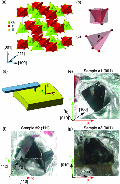
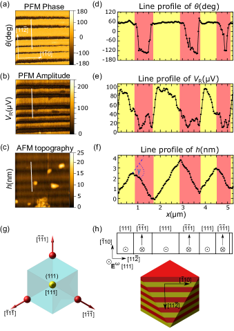
GaV4S8 belongs to the family of lacunar spinels, characterized by the vacancy of every second Ga-site in the unit cell as compared to the ordinary spinel structure. In an ideal spinel structure, the vanadium atoms would be arranged in a network of corner-sharing tetrahedrons, known as the phyrochore lattice. However, owing to the central cationic void in every second tetrahedron, the lattice decomposes into smaller and larger V4 tetrahedral clusters, hence forming a breathing pyrochlore lattice [17]. As shown in Fig. 1 (a), the smaller V4 clusters constitute an fcc lattice. Each V4 cluster carries a spin of S=1/2, since the triply degenerate cluster orbital is occupied by single unpaired electrons [18]. The orbital degeneracy is lifted via a cooperative Jahn-Teller distortion at through the stretching of the lattice along any of the four -type body diagonals in the pseudocubic system, as presented in Figs. 1 (b) and (c), reducing the crystal symmetry from non-centrosymmetric cubic (F3m) to polar rhombohedral (R3m) [18, 19]. The electric polarization developing upon the Jahn-Teller transition is confirmed by recent pyrocurrent measurements [16]. Dielectric spectroscopy [20] and specific heat measurements [21] imply that the ferroelectric transition in GaV4S8 is not displacive but of disorder-to-order type. Since the symmetry is lost upon this transition and the Td point symmetry is reduced to its subgroup C3v, the formation of four degenerate structural domains is allowed. The polarization in each structural domain is aligned parallel to one of the four axes of distortion. More specifically, local electric dipoles on all V4 tetrahedra within a given domain point towards the same vertex, as shown in Fig.1 (c). Since the inversion symmetry is already broken in the cubic F3m phase, +/- polarization domains cannot arise within a single inversion variant of the crystal.
Note that throughout this study, the structural domains will be labelled by the direction of the local polarization, such as [111], [1], [1], [1], as displayed in Figs. 3 (g) and 5 (g). Although these domains represent only one of the two possible inversion variants, all arguments in this paper can be equally applied to the other inversion variant by reversing the sign of the polarization vectors.
In addition to its ferroelectric nature, GaV4S8 becomes magnetically ordered [18, 22, 23] and thus multiferroic at TC = 13 K [24, 16]. Magnetization measurements revealed several magnetic phases [25] that have been recently identified as the cycloidal state and the Néel-type skyrmion lattice (SkL) embedded in the ferromagnetic state [24]. The axial symmetry of the rhombohedral structure gives rise to an orientational confinement of the skyrmion cores in each domain along the magnetic easy-axis, which coincides with the direction of the Jahn-Teller distortion or equivalently the direction of the ferroelectric polarization. Due to the change in the orientation of skyrmion cores from domain to domain, the size of a consistent SkL must be limited by the size of the structural domain. Small-angle neutron scattering data indicate the lateral correlation length of the skyrmion lattice to be larger than 110 nm [24], though the actual value cannot be determined due to the resolution limit of the experiment. Clearly, the ultimate upper limit of the correlation length is set by the size of the structural domains. The local-scale investigation of these domains characterized by their size, shape and orientation is exactly the subject of the present study. Polar and magnetic orders are cross-coupled in GaV4S8, which leads to a different ferroelectric polarization in each magnetic phase [16]. This suggests that Néel-type skyrmions in GaV4S8 carry electric polarization providing an intriguing potential for the detection and manipulation of individual skyrmions by means of local electric probes, such as scanning probe techniques or nano-circuits.
Results
Typical PFM micrographs recorded at the same position on the (001) plane of the first GaV4S8 sample, referred to as Sample #1 in Fig. 1 (e), at and are shown in Fig. 2. The size of the scanned area was approximately 10 m 10 m, the difference in the length scales at the two temperatures are due to the temperature-dependent response of the piezo actuator, which was calibrated at T=50 K.
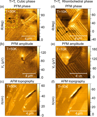
Since GaV4S8 has a non-centrosymmetric lattice even at high temperatures, in principle, antiphase or inversion domains could be present. In such antiphase domains, the magnitude of the converse piezoelectric effect is the same but has the opposite sign. However, this configuration is not appropriate to detect inversion domains, as the F3m crystal symmetry above the Jahn-Teller transition dictates the vanishing of the measured component of the converse piezoelectric tensor, (see supplementary information for details). Here, the direction indicated in the upper index refers to that of the AFM tip, the lower two entries denote the -element of the tensor probed in the cubic (’c’) phase of the crystal. This in accord with the structureless PFM images in Figs. 2 (a)-(b) obtained at .
PFM images taken at , below the Jahn-Teller transition, reveal the appearance of stripe domains, that were analyzed both for the phase and amplitude dependence of the PFM signal [see Figs. 2 (d) and (e), respectively]. As shown, the width of the ferroelectric domains ranges from 200 - 300 nm. The same typical domain sizes have been found in other scanning areas of the (001) surface (see Supplementary Information for more images). Irregularities in the alternating domain structure are observed close to the center of the image due to a topographic defect. Static voltages up to 10 V applied between the sample and the tip did not indicate any local polarization switching. Even though the ordered magnetic states were shown to carry sizable magnetoelectric polarization [16], the lateral resolution of the PFM measurement, approximately 50 nm, is not sufficient to resolve the polarization pattern accompanying the nanometric magnetic modulations.
The topography images of the scanned areas obtained from the dc component of the AFM signal were acquired together with the modulated PFM signals both at and , as shown in Figs. 2 (c) and (f), respectively. Besides the contrast observed in the PFM images, the topography image also reveals the presence of structural domains in the rhombohedral phase due to the different surface inclinations of the lattice in adjacent domains. The faint contrast seen in Fig. 2 (f) appears more pronounced in an area without any topographic defects as in Fig. 3 (a) and (d). Note that such a saw-tooth height profile typical to the lamellar domain patterns in GaV4S8, was already observed in AFM micrographs by Kézsmárki et al. [24].
The Jahn-Teller distortion leads to the appearance of a piezo-response, manifested by the component, where the entry ’r’ stands for the rhombohedral phase of the crystal. Whereas the magnitude of this element is equal in all rhombohedral domains, its sign is determined by the sign of , the polarization component normal to the probed surface. Thus, the four domains can be divided into two pairs of opposite component: [111], and ,. In the PFM phase signal, , a 180∘ contrast inversion is expected between these pairs, whereas, the PFM amplitude, is expected to be equal for all domains. The electromechanical coupling between the tip and the bottom electrode, however, results in an appreciable background signal (see Methods) affecting both the relative phase and amplitude of the PFM signals [26].
Figures 3 (a)-(c) display the PFM phase and amplitude images along with the AFM topography image recorded in the area indicated by the yellow dashed rectangle in Fig. 2 (a). The PFM amplitude and phase maps are displayed background-corrected as described in the Methods section. Figures 3 (d)-(f) demonstrate the profiles of the three channels along the same identical line cut out perpendicular to the domain boundaries, as marked by white bars in each figure. The alternating domain structure along the profile can be easily traced both in the AFM topography and PFM channels. As seen, the ferroelectric as well as ferroelastic domain boundaries are reflected by the reversal of the inclination angle in the topographic profile and by the 180∘ phase shift of the PFM signal and the minimum in its magnitude.
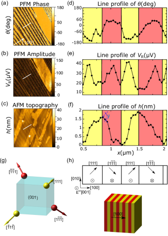
The measured piezo-response falls within the range of 20-40 V, corresponing to displacements of 6-12 pm as determined from the calibration of the -displacement of the AFM tip. The driving voltage was 10 Vpp, therefore the magnitude of the -element is estimated to be in the range of 1-2 pm/V.
The total inclination angle between the surfaces inferred from the AFM topography profile, indicated by dashed blue arcs in Fig 3. (f), yields a value of approximately . This value is in good agreement with the rhombohedral angle of , as measured by X-ray diffraction at [18], which corresponds to (for details, see SI).
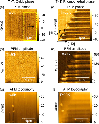
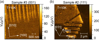
In order to gain insight into the three-dimensional orientation of the domain walls, PFM measurements were carried out also on the (111) surface of GaV4S8 Sample #2 [Fig. 1 (f)] at various temperatures. Figures 4 (a)-(c) display the PFM phase, PFM amplitude and AFM images, respectively, measured at . Figures 4 (d)-(f) present the same maps, captured over the same area with the sample cooled to . Similarly to the findings for the (001) plane, the PFM scans reveal stripe domain patterns in the rhombohedral phase, vanishing at temperatures above the structural phase transition.
In contrast to the (001)-plane scans, the component of the converse piezoelectric tensor is allowed by the F3m symmetry, having opposite signs for the two antiphase domains. The vanishing PFM contrast in the high-temperature phase, however, suggests that the observed rhombohedral domains belong to the same inversion variant. Indeed, none of the high-temperature measurements on the (111) plane revealed any sign of antiphase domain boundaries (see Supporting Information). Therefore, it is reasonable to assume that the domain size of a pure inversion variant is large as compared to the scanned area, possibly extending over the whole crystal. The domain wall spacing measures approximately , being much broader than those observed on the (001) plane. However, one additional stripe seems to be present within each larger domain, indicating a finer sub-structure. Also note that depending on the orientation of the domain walls the actual width of the domains might be smaller than the values determined from their (111)-sections observed here. The actual orientation of the domain walls will be discussed later.
Figures 5 (a)-(c) present the background-corrected PFM phase and amplitude channels along with the AFM topography image recorded on the area marked by the yellow dashed rectangle in Fig. 4 (a). Figures 5 (d)-(f) display the profiles along the white lines parallel to , as indicated in the images in the left panels. The domain boundaries are clearly visible in all three channels.
PFM measurements on the (111) plane in the rhombohedral phase are sensitive to the contrast in the converse piezoelectric constants between the unique domain and the three other domains , , , whose elements are equivalent. In theory, the contrast between the piezo-response of the two distinguishable domain types yields a ratio of , where the negative sign indicates a shift in the PFM phase.
The magnitude of the piezoelectric vibrations measured on the (111) plane is 80-100 V for domain [111] and 30-40 V for the other three domains. The corresponding value of is 2.5-5 pm/V. This tensor element involves contributions from , and (See Supplementary Information for details), which accounts for the enhancement in the PFM signal.
The inclination of the (111) surface between the (111) domain and any of the three other domains is expected to be from the degree of rhombohedral distortion determined by X-ray diffraction [18] (for details see SI). The opposing surface inclination in the alternating domains is clearly discernable from the AFM topography images [see Figs. 4 (f) and 5 (a)-(d)], though the measured angle, , is somewhat lower than the predicted value.
Discussion
In a ferroelectric crystal the energy minimum is realized as an equilibrium between the cost of domain wall formation and the gain through the reduction in the stray field with increasing number of domains coexisting in the material [27, 28]. The mechanical continuity and electric neutrality of the interfaces between adjacent domains dictate a set of so-called compatibility equations [27]. In neighboring rhombohedral domains that belong to the same inversion variant, the polarization vectors parallel to the -axes span approximately 109∘. For such rhombohedral domains, the compatibility criteria require that domain walls lay in (001)-type planes [27].
A global energy minimum is typically achieved by the organization of the structural variants into alternating laminate patterns, as described by Tsou et al. [28, 29]. Regular domain patterns observed in most ferroelectrics can be understood and classified by their model.
Indeed, all PFM images taken both on the (001) and the (111) planes of GaV4S8 reveal lamellar domain structures. In case of Sample #1 (Figs. 2 and 3), the normal vectors of the observed domain walls correspond to a -type pseudocubic direction of the crystal, where the component cannot be unambiguously determined from the measurement on this single surface. However, , corresponding to (100)-type domain walls is consistent with the compatibility criteria and separates structural domains originating from the same high-temperature inversion variant. In this case, the alternation of [111]- and [1]-type (Figs. 3 (g) and (h)) or []- and [1]-type variants (not shown) can be attributed to the observed lamellar domain structures. The two domains in any of the above pairs produce a PFM contrast measured on the (001) surface, represented by yellow and red colors in the figures. The measurement of the out-of-plane deformation does not allow for any further distinction between these two possible domain pairs. In the PFM measurements on Sample #2, stripes parallel with the -type edges of the triangle-shaped (111) surface have been evidenced [Figs. 4 and 5]. Such patterns can be explained again as compatible domain walls parallel to the (001) plane, which are projected to the (111) surface, as presented in Figs. 5 (g) and (h). The possible compatible domain pairs can be either [111] with [] or [1] with []. However, PFM measurements on the (111) plane only reveal contrast in the former case, visualized by the yellow and red coloring in Figs. 5 (g) and (h). Within the dark area in the top left corner of the PFM amplitude image in Fig 4 (e), an alternating structure of variants [1] and [] must be present in order to maintain compatibility along the domain boundaries. Although these variants are indistinguishable via an out-of-plane PFM measurement, their presence can be traced in the PFM phase image [Fig. 4 (d)] owing to the small contribution of the in-plane piezo-response to the measurement as a result of the non-uniform electric fields emerging near the tip.
We note that (110)-type domain walls could also account for similar patterns both in the (001) and (111) planes. However, the electric neutrality of such domain walls would require a 71∘ angle between the polarization of the adjacent domains [27], which belong to high-temperature parent variants with an inverted structure. In the present experiments no sign of antiphase domains has been confirmed by PFM measurements above the temperature of the structural transition, moreover, the formation of lamellae of inversion variants at high-temperatures during the growth process seems rather unlikely. Thus our experiments show that the structural domain walls in GaV4S8 are parallel to (100)-type planes. Consequently, the actual distances between the (100)-type domain-walls in the bulk crystal are smaller by a factor of than those observed on a (111) surface.
Figures 6 (a) and (b) present PFM amplitude images of the (001) and (111) surface of GaV4S8, respectively, captured in the rhombohedral phase close to the ends of the stripe domain patterns. Transitions of lamellar structures into another pair of alternating domains or to a uniform crystal variant may occur whenever the new phase starts developing from several nucleation centers such as structural defects. Epilayer plateaus may also serve as natural endings of lamellar structures. The resulting domain boundaries are prone to mechanical and electrostatic incompatibilities. Figure 6 (a) reveals needle-like domain endings in an alternating structure as a consequence of mechanical stress and electrostatic repulsion induced at the incompatible domain walls [30]. Additionally, more complex domain patterns can arise as a manifestation of adjoining lamellae, as seen in Fig. 6 (b). Thus, for future studies, it will be interesting to explore these domain boundaries more into depth, e.g. performing conducting AFM measurements in order to trace whether or not the compatibility criteria are broken, and whether these domain walls might possibly be rendered conductive.
Conclusion
We have detected ferroelectric-ferroelastic domains in the rhombohedral phase of GaV4S8 via simultaneous out-of-plane PFM and AFM topographic measurements. Lamellar domain structures have been observed and identified through alternating pairs of structural domains, belonging to a single inversion variant of the crystal. The magnitude of the piezoresponse measured on (001) and (111) faces of the crystals ranges within 1-5pm/V. Based on the mechanical and electric compatibility criteria we showed that the domain walls are parallel with (100)-type planes. The collection of PFM images supports that the compatibility criteria of non-charged domain walls are generally satisfied and also indicates the lack of antiphase domains in the crystals studied here. Notably, local incompatibilities have been encountered at the endings of the lamellar patterns, claiming for charged domain walls and polytype domain structures.
The typical thickness of the observed lamella-like domains is in the range of 100 nm -1.2 m (see SI for details). The wavelength of the cycloidal modulation and the diameter of Néel-skyrmions in GaV4S8 were reported to be 20 nm [24], at least one order of magnitude smaller than the thickness of the observed ferroelectric domains. Hence, the lateral correlation length of the skyrmion lattice may be limited by the structural domain size, however, the stability of the skyrmions is not affected by the thickness of the domains. On the other hand, the correlation length along the skyrmion tubes, i.e. perpendicular to the 2-dimensional lattice, which were found to be of 540 nm [24], is likely limited by the size of the rhombohedral domains. Since skyrmion cores are oriented along the polar axes of the ferroelectric domains, individual skyrmions are expected to be confined within the lamellar domains. We expect that engineering the ferroelectric domain patterns in polar skyrmion host materials provides a new route to tune, confine and manipulate skyrmions in bulk 3D materials.
Methods
Single crystals of GaV4S8 were grown via chemical vapour transport method as reported elsewhere [24]. The typical dimensions of the cuboid-shaped crystals are 1-2 mm [see Fig. 1 (e)-(g)]. The high quality of the samples has been confirmed by X-ray diffraction and specific heat measurements.
The mapping of the nanoscale topography and the local piezo-response were performed with a custom-made low-temperature AFM [31, 32] on as-grown (001) and (111) surfaces of single crystalline GaV4S8 samples [see Figs. 1 (e)-(g)]. Commercial platinum-iridium coated silicon tips with a tip radius of about 30 nm were used. An ac voltage of 5 V at 22.3 kHz was applied between tip and sample during contact-mode scans, with the cantilever deflection signal being demodulated at that same frequency by a lock-in amplifier to obtain the out-of-plane PFM amplitude and phase signals (note that the sample surface topography is recorded always simultaneously to PFM mapping). Due to the interferometric detection in our LT-PFM setup, only the out-of-plane element of the converse piezoelectric tensor was measured, where the direction always points normal to the sample surface in our notation [see Fig. 1 (d)].
In theory, structural domains with opposite signs of , i.e. the -component of their polarization vector, feature a 180∘ phase contrast, whereas the amplitude of the PFM signal is proportional to the magnitude of [33, 34]. Besides the intrinsic PFM signal, the electromechanical coupling between the tip and the bottom electrode leads to an oscillation of the tip as well, manifested as a background signal of arbitrary phase with respect to the intrinsic PFM response. Hence, a PFM contrast between the domains emerges both in the phase and the amplitude channels, as seen in Figs. 2 (d) and (e). The parasitic baseline signal is typically commensurate with the piezo-response of the sample [26, 35, 36, 37]. The magnitude of the surface vibrations () originating exclusively from the converse piezoelectric effect can be estimated from the demodulated PFM amplitude and phase maps via background subtraction in the complex plane [26]. In case of measurements performed on the (001) surface, the magnitude of the piezo-response is equal in all the four domains (for details, see SI), requiring that the complex PFM signal must be symmetric to zero. Hence, the complex components of the baseline, and , are determined as the spatial average values of the measured in-phase () and out-of-phase component () of the PFM signal: and . As a result, the background-corrected signal becomes symmetric to the origin of the complex plane. The magnitude and the phase of the surface piezoelectric vibration thus can be expressed as [26]:
| (1) | |||
In case of experiments performed on the (111) surfaces, the magnitude of the probed piezo-response component of the [111]-domain, is expected to be three times larger as compared to the other three domains (see Supplementary Information). Therefore, the baseline correction in Equation 1 is employed using the modified and complex background components, where and are the average of the maximal and minimal amplitudes in the X and Y channels, respectively.
References
- [1] Xu, Y. Ferroelectric materials and their applications (Elsevier, 2013).
- [2] Catalan, G., Seidel, J., Ramesh, R. & Scott, J. F. Domain wall nanoelectronics. Reviews of Modern Physics 84, 119 (2012).
- [3] Meier, D. Functional domain walls in multiferroics. Journal of Physics: Condensed Matter 27, 463003 (2015).
- [4] Seidel, J. et al. Conduction at domain walls in oxide multiferroics. Nature materials 8, 229–234 (2009).
- [5] Sluka, T., Tagantsev, A. K., Bednyakov, P. & Setter, N. Free-electron gas at charged domain walls in insulating \ceBaTiO3. Nature communications 4, 1808 (2013).
- [6] Schröder, M. et al. Nanoscale and macroscopic electrical ac transport along conductive domain walls in lithium niobate single crystals. Materials Research Express 1, 035012 (2014).
- [7] Kagawa, F. et al. Dynamics of multiferroic domain wall in spin-cycloidal ferroelectric \ceDyMnO3. Physical review letters 102, 057604 (2009).
- [8] Meier, D. et al. Anisotropic conductance at improper ferroelectric domain walls. Nature materials 11, 284–288 (2012).
- [9] Cheong, S.-W. & Mostovoy, M. Multiferroics: a magnetic twist for ferroelectricity. Nature materials 6, 13–20 (2007).
- [10] Spaldin, N. A. & Fiebig, M. The renaissance of magnetoelectric multiferroics. Science 309, 391–392 (2005).
- [11] Kimura, T. et al. Magnetic control of ferroelectric polarization. nature 426, 55–58 (2003).
- [12] Kezsmarki, I. et al. One-way transparency of four-coloured spin-wave excitations in multiferroic materials. Nature communications 5 (2014).
- [13] Lilienblum, M. et al. Ferroelectricity in the multiferroic hexagonal manganites. Nature Physics 11, 1070–1073 (2015).
- [14] Barone, P., Yamauchi, K. & Picozzi, S. Jahn-teller distortions as a novel source of multiferroicity. Physical Review B 92, 014116 (2015).
- [15] Xu, K. & Xiang, H. Unusual ferroelectricity induced by the jahn-teller effect: A case study on lacunar spinel compounds. Physical Review B 92, 121112 (2015).
- [16] Ruff, E. et al. Multiferroicity and skyrmions carrying electric polarization in \ceGaV4S8. Science advances 1, e1500916 (2015).
- [17] Okamoto, Y., Nilsen, G. J., Attfield, J. P. & Hiroi, Z. Breathing pyrochlore lattice realized in a-site ordered spinel oxides \ceLiGaCr4O8 and \ceLiInCr4O8. Physical review letters 110, 097203 (2013).
- [18] Pocha, R., Johrendt, D. & Pöttgen, R. Electronic and structural instabilities in \ceGaV4S8 and \ceGaMo4S8. Chemistry of materials 12, 2882–2887 (2000).
- [19] Hlinka, J. et al. Lattice modes and the jahn-teller ferroelectric transition of \ceGaV4S8. Phys. Rev. B 94, 060104 (2016).
- [20] Wang, Z. et al. Polar dynamics at the jahn-teller transition in ferroelectric \ceGaV4S8. Phys. Rev. Lett. 115, 207601 (2015).
- [21] Malik, V., Yadav, C., Rastogi, A. & Kumar, D. Peculiar magnetism of transition metal cluster compounds. EPL (Europhysics Letters) 101, 67008 (2013).
- [22] Müller, H., Kockelmann, W. & Johrendt, D. The magnetic structure and electronic ground states of mott insulators \ceGeV4S8 and \ceGaV4S8. Chemistry of materials 18, 2174–2180 (2006).
- [23] Yadav, C., Nigam, A. & Rastogi, A. Thermodynamic properties of ferromagnetic mott-insulator gav4s8. Physica B: Condensed Matter 403, 1474–1475 (2008).
- [24] Kézsmárki, I. et al. Néel-type skyrmion lattice with confined orientation in the polar magnetic semiconductor \ceGaV4S8. Nature materials 14, 1116–1122 (2015).
- [25] Nakamura, H. et al. Low-field multi-step magnetization of \ceGaV4S8 single crystal. In Journal of Physics: Conference Series, vol. 145, 012077 (IOP Publishing, 2009).
- [26] Jungk, T., Hoffmann, Á. & Soergel, E. Quantitative analysis of ferroelectric domain imaging with piezoresponse force microscopy. Applied physics letters 89, 163507 (2006).
- [27] Shu, Y. & Bhattacharya, K. Domain patterns and macroscopic behaviour of ferroelectric materials. Philosophical Magazine B 81, 2021–2054 (2001).
- [28] Tsou, N. & Huber, J. Compatible domain structures and the poling of single crystal ferroelectrics. Mechanics of Materials 42, 740–753 (2010).
- [29] Tsou, N., Potnis, P. & Huber, J. Classification of laminate domain patterns in ferroelectrics. Physical Review B 83, 184120 (2011).
- [30] Salje, E. K., Buckley, A., Van Tendeloo, G., Ishibashi, Y. & Nord, G. L. Needle twins and right-angled twins in minerals: comparison between experiment and theory. American Mineralogist 83, 811–822 (1998).
- [31] Döring, J., von Ribbeck, H.-G., Fehrenbacher, M., Kehr, S. C. & Eng, L. M. Near-field resonance shifts of ferroelectric barium titanate domains upon low-temperature phase transition. Applied Physics Letters 105, 053109 (2014).
- [32] Döring, J., Eng, L. M. & Kehr, S. C. Low-temperature piezoresponse force microscopy on barium titanate. Journal of Applied Physics 120, 084103 (2016).
- [33] Jungk, T., Hoffmann, Á. & Soergel, E. Contrast mechanisms for the detection of ferroelectric domains with scanning force microscopy. New Journal of Physics 11, 033029 (2009).
- [34] Kalinin, S. V. et al. Recent advances in electromechanical imaging on the nanometer scale: Polarization dynamics in ferroelectrics, biopolymers, and liquid imaging. Japanese Journal of Applied Physics 46, 5674 (2007).
- [35] Xu, C., Woo, C., Shi, S. & Wang, Y. Effects of frequencies of ac modulation voltage on piezoelectric-induced images using atomic force microscopy. Materials characterization 52, 319–322 (2004).
- [36] Jungk, T., Hoffmann, A. & Soergel, E. Consequences of the background in piezoresponse force microscopy on the imaging of ferroelectric domain structures. Journal of microscopy 227, 72–78 (2007).
- [37] Bo, H. et al. Influence of feedback parameters on ferroelectric domain imaging with piezoresponse force microscopy. Review of Scientific Instruments 81, 043704 (2010).
Acknowledgement
The authors thank J. Hlinka for the enlightening discussions, and the Helmholtz-Zentrum Dresden-Rossendorf, Germany for providing lab space, technical support, and the required cryogenics. The work was supported by the Deutsche Forschungsgemeinschaft via the collaborative research center TRR 80 (Augsburg, Munich, Stuttgart), the Cluster of Excellence ’Center for Advancing Electronics Dresden (cfaed)’, the Collaborative Research Center ’Correlated Magnetism: From Frustration to Topology’ (SFB 1143) via TP C05, and through Project No. KE2068/2-1, by the Hungarian Research Funds OTKA K108918, PD 111756, and Bolyai 00565/14/11 as well as by the BMBF under Grants No. 05K10ODB and 05K16ODA.
Author Contributions
J.D., A.B., S.B. performed the PFM measurements. A.B., S.B. analysed and interpreted the data. V.T. synthesized the crystals. A.B. wrote the manuscript with contributions from S.B. and I.K. S.B. supervised the project. The PFM setup was developed by S.K, J.D., L.M.E. All authors discussed and commented on the content of the paper.
Competing interests
The authors declare no competing financial interests.