Electrical Detection of Individual Skyrmions in Graphene Devices
Abstract
We study a graphene Hall probe located on top of a magnetic surface as a detector of skyrmions, using as working principle the anomalous Hall effect produced by the exchange interaction of the graphene electrons with the non-coplanar magnetization of the skyrmion. We study the magnitude of the effect as a function of the exchange interaction, skyrmion size and device dimensions. Our calculations for multiterminal graphene nanodevices, working in the ballistic regime, indicate that for realistic exchange interactions a single skyrmion would give Hall voltages well within reach of the experimental state of the art. The proposed device could act as an electrical transducer that marks the presence of a single skyrmion in a nanoscale region, paving the way towards the integration of skyrmion-based spintronics and graphene electronics.
I Introduction
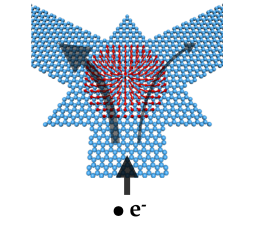
Skyrmions are magnetic non-coplanar spin textures that are attracting a great deal of attention for both their appealing physical propertiesRoszler et al. (2006) and their potential use in spintronicsDuine (2013); Rosch (2017); Dupé et al. (2016); Edi (2013). They have been observed forming lattices in a variety of non-centrosymmetric magnetic crystalsMühlbauer et al. (2009); Münzer et al. (2010); Yu et al. (2012); Tokunaga et al. (2015), including insulating materials such as the chiral-lattice magnet Cu2OSeO3Seki et al. (2012); Langner et al. (2014); Zhang et al. (2016). They also form two dimensional arrays in atomically thin layers of Fe deposited on Ir(111)Heinze et al. (2011); Romming et al. (2015). In these systems the spins typically feel a competition between aligning with their neighbors and being perpendicular to them, what favors chiral ordering. A variety of interactions can assist non-collinear arrangements, including Dzyaloshinskii-Moryia interactions, dipolar interactions and frustrated exchange interactions and the size of an individual skyrmion can range from 1 nm to 1 m depending on which specific mechanism is involved. To date, these magnetic structures are detected by means of neutron scatteringMühlbauer et al. (2009), electron microscopyYu et al. (2010) and even individually, with atomic scale resolution, by means of spin polarized scanning tunneling microscopyPfleiderer (2011); Heinze et al. (2011) and atomic size sensorsDovzhenko et al. (2016).
The particle-like nature of skyrmions has motivated proposals to use them as elementary units to store classical digital information, inspired by the magnetic domain-wall racetrack memoriesParkin et al. (2008). Such a perspective has become increasingly attractive since it has been experimentally provedRomming et al. (2015) the possibility of manipulating two-dimensional magnetic lattices by creating and destroying individual skyrmions by means of spin-polarized currents in STM devices. This, along with the experimental findingJonietz et al. (2010) of skyrmion motion driven by ultralow current densities of the order of A m-2, considerably smaller than those needed for domain wall motion in ferromagnets, makes skyrmions potentially optimal candidates for the next generation of magnetoelectronic readout devices.
Mathematically, skyrmions are topologically non-trivial objects whose topology content is embedded in an index, the winding number , defined as
| (1) |
where is a classical magnetization field and the two-dimensional integral is performed over the overall area occupied by the skyrmion. The winding number can only acquire integer values, and a skyrmion is distinguished from other topologically trivial magnetic textures for exhibiting a non-zero value of the integer . The magnetization field of a skyrmion can be expressed as a mapping from the polar plane coordinates to the unit sphere coordinates
| (2) |
provided the spin configuration at is -independent so that it can be mapped to a single point on the sphere. The mapping is specified by the two functionsNagaosa and Tokura (2013):
| (3) |
and varies from for large to as we approach , the core of the skyrmion. Here we adopt the following model:
| (4) |
where is the skyrmion winding number introduced in (1), is a phase termed helicity that can be gauged away by rotation around the -axis, and is a function of the radial coordinate that describes a smooth radial profile inside of the skyrmion radius . Such a texture describes a magnetic configuration where the spins are all aligned perpendicular to the film plane with the exception of those comprised within the radius where they all progressively align along the anti-parallel direction, that is picked up exactly at . The condition that the spins at and are oppositely oriented is crucial in order to ensure a non-trivial topology of the magnetic texture.
Several recent theoretical worksHamamoto et al. (2015); Yin et al. (2015); Lado and Fernández-Rossier (2015) point out that two-dimensional systems coupled either weakly or strongly to individual skyrmions or skyrmionic lattices can develop an Anomalous Hall (AH) or Quantum Anomalous Hall (QAH) phase owing to the non-trivial topology of these structures in real space. This effect refers to the onset of a transverse Hall response arising in magnetic systems driven by anomalous velocities, associated to Berry curvature, without the need of an applied magnetic fieldNagaosa et al. (2010). This anomalous Hall response can be either of extrinsic or intrinsic nature. In the case of proximizing a pristine 2D system with magnetic skyrmions, the generation of a transverse voltage is of extrinsic nature and ascribable to the imprinting of the skyrmions real space topology onto the (trivial) reciprocal space topology of the non-magnetic systemLado and Fernández-Rossier (2015). Based on these findings, along with a recent work demonstrating the possibility of growing a graphene flake on top of a single atomic layer of Fe on a Ir(111) substrateHamamoto et al. (2015); Brede et al. (2014), here we consider graphene flakes weakly coupled to magnetic films as skyrmion detectors. To this aim, we compute the skewness of the scattering and the associated Hall signal induced in a graphene island coupled to a single skyrmion within a multi-terminal geometry. Graphene unique properties are ideal to implement the proposed device. As a fact, being atomically thin maximizes proximity effects, making it an optimal material to grow on top of magnetic materials. Furthermore, the fabrication of high quality graphene electronic devices both at the micron and nanometer scale is absolutely well demonstrated Banszerus et al. (2016); Freitag et al. (2016); Shalom et al. (2016) and its use as a magnetic sensor for magnetic adsorbates has been already tested experimentallyCandini et al. (2011a, b) and studied theoreticallyGonzález et al. (2013).
The paper is organized as follows. In section II we discuss a 2D Dirac system in the continuum coupled to a non-uniform spin texture and performing a standard rotation in spin space we unveil two types of influence on the Dirac electrons. In section III we introduce Landauer’s formalism for quantum transport on the lattice and describe the setup of the proposed Hall experiment. Finally, in section IV, we discuss the results obtained by applying Landauer’s formula to a graphene flake coupled to a single skyrmion, characterizing the Hall conductance as a function of several parameters and comparing the effectiveness of graphene with that of a standard two-dimensional electron gas (2DEG).
II Analytic approach in the continuum
In this section we describe graphene electrons interacting with a non-coplanar magnetization field , as given by equation (2), using a 2D Dirac Hamiltonian:
| (5) |
with the vector of Pauli matrices acting in spin space and the vector of Pauli matrices acting in pseudo-spin space. We perform a rotation of the Hamiltonian so that in every point of space the spin quantization axis is chosen along the direction of the spin texture . As a result, the representation of the exchange term is diagonal in the rotated frame, but the Dirac Hamiltonian acquires new terms that encode the influence of the exchange interaction of the Dirac electrons with the non-coplanar field. The unitary matrix that performs such a transformation in the basis is
| (6) |
where
| (7) |
The transformed Hamiltonian reads
| (8) |
with
| (9) |
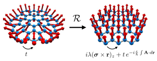
and , . In the rotated reference frame, the exchange term is manifestly diagonal. Besides, the Hamiltonian has acquired additional kinetic terms. The field acts as a spin-dependent gauge vector potential that couples with the momenta of the Dirac electrons, whereas the remaining two terms closely resemble a spin-orbit (SO) interaction of the Rashba type. On the lattice, this corresponds to mapping a system characterized by a non-collinear exchange field and real hopping to a ferromagnetic system with a purely imaginary hopping mimicking the effect of SO coupling plus a complex hopping supported by a gauge field entering as a Peierls phase. This is schematized in figure 2.
From the gauge field, one can compute the effective magnetic field acting on the system as
| (10) |
that reads
| (11) |
This transformation of the Hamiltonian therefore allows to interpret the topological content embedded in the skyrmion texture as a superposition of two effects: (i) The generation of an effective emergent electromagnetic field (EEMF) described by the gauge potential ; (ii) The coexistence of ferromagnetic exchange with a Rashba-like SO interaction, what has been predicted to give rise to a QAH phase Qiao et al. (2010). Both ingredients are endowed with a topological character that the skyrmion texture is able to imprint onto the Dirac electrons and are therefore responsible for generating a Hall response in the system. An analog result has been derivedNagaosa-Tokura13 for Schrodinger electrons, with the remarkable difference that in the strong coupling limit () the spin-mixing terms vanish and the problem is exactly mapped to a spinless one-band system where the electrons momenta are coupled to a vector potential describing an emergent magnetic field. In the case of Dirac electrons, the spin-mixing term survives at all coupling regimes and the mapping to a pure EEMF is an incomplete description of the physics taking place in the system. Whereas this picture provides some physical insight of what happens to graphene Dirac electrons surfing a skyrmions, it does not provide a straightforward method to compute the Hall response.
III Tight-binding quantum transport approach
In this section we overview the quantum transport methodology that we will employ to compute the Hall response induced by an individual magnetic skyrmion in a graphene device. Importantly, we are implicitly assuming that the substrate material is an insulating skyrmion crystal such as CuGeO3Šljivančanin et al. (1997) and Cu2OSeO3Seki et al. (2012); Langner et al. (2014); Zhang et al. (2016) in such a way that the current only flows through graphene.
The graphene electrons are described with the standard tight-binding Hammiltonian for the honeycomb lattice with one orbital per atomCastro Neto et al. (2009), plus their exchange interaction with the classical magnetization of the skyrmion :
| (12) |
Here is the classical continuous magnetization texture (2) discretized over the graphene lattice and taken at site and is the vector whose components are the Pauli matrices acting in spin space associated with the -th lattice site. The symbol implies summation over all nearest neighboring pairs of atoms, and we are assuming that the magnitude of the magnetization is uniform over the whole graphene lattice. This Hamiltonian has been considered beforeLado and Fernández-Rossier (2015) for the case of 2D graphene interacting with a skyrmion crystal. In contrast, here we consider a graphene device that hosts an individual skyrmion.
The mathematical framework that we use to study quantum transport is based on Landauer’s formalism for conductanceLandauer (1957). Given an experimental setup where a device is attached to metallic contacts, Landauer’s multi-terminal technique allows to compute the transmission amplitude between the -th and the -th contact from the relation
| (13) |
where and are respectively the retarded and advanced Green’s functions of the device, that is the Green’s function of the isolated device corrected by the self-energies of the leads
| (14) |
where is the Hamiltonian of the isolated device. The ’s are quantities associated to the leads’ selfenergies as . The leads’ self-energies incorporate the coupling between the device and the leads as , with the surface Green’s function Sancho et al. (1985) of the -th lead, and the hopping matrix between the device and the -th lead. From the knowledge of the transmission amplitudes, the expression for the total current flowing from the lead follows straightforwardly:
| (15) |
with the Fermi distribution function, so that at zero temperature the previous expression reduces to and for a sufficiently small energy interval one can expand the transmission coefficient around the Fermi energy and stick to zeroth order. By doing so, one finally finds that the formula for the current flowing from the lead becomes:
| (16) |
This equation can be used to derive the Hall response in a given multiterminal device in two different ways. In both cases, the first step of the calculation is the numerical determination of the transmission coefficients . Then we can either impose (i) the voltage drops , defined as the difference between the chemical potentials of the different electrodes, and compute the resulting current (inverse Hall effect), or (ii) impose a longitudinal current flow and a null transverse current, find the resulting chemical potentials and determine the Hall response (direct Hall effect).
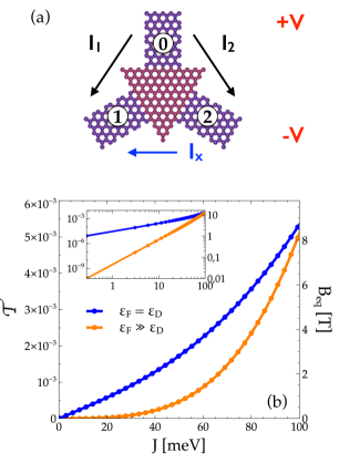
When the methods just described are implemented in an ordinary four-terminal geometryYin et al. (2015), the resulting relation between the Hall conductance and the transmission coefficients is far from intuitive. In this paper, for the sake of simplicity, we consider a three terminal device (TTD) of the kind of the one shown in figure 3a. We choose to fix the chemical potentials of the three electrodes, labeled as , and , and compute the resulting current. Specifically, we impose that and . In this way, the voltage difference between leads 1 and 2 is automatically set to zero whereas the voltage difference between lead 0 and leads 1,2 is . The expression for the current flowing from leads 1 and 2 is for . From this expressions it is straightforward to deduce the current imbalance , that reflects the presence of a transverse force, , whence our definition of Hall conductance in this geometry
| (17) |
In the following we present the numerical results for the normalized transmission imbalance, that is
| (18) |
in order to work with quantities that do not depend on the number of conduction channels in the device. This 3-terminal setup simplifies considerably the analysis of the numerical results, and also matches the symmetry of the graphene lattice. However, in a real device, disorder and contact asymmetries might result in additional transmission imbalances that might obscure the detection of skyrmions. Thus, in real devices a standard 4 terminal geometry should be used, given that the principles and magnitude of the physical effect are expected to be the same.
IV Results and discussion
We now present the results obtained by calculating the imbalance in the transmission coefficients eq. (18) for a graphene quantum dot coupled to a skyrmion. For a better physical insight, we provide an estimate for the equivalent magnetic field that would give rise to a conventional Hall response of the same magnitude of that induced by the skyrmion. Details on the determination of such a field are given in the Appendix. In the following we consider flakes sizes of the order of nm2, and skyrmions with radius of the order of 2-3 nm and winding number . Also, we are solely interested in realisticWei et al. (2016); Yang et al. (2013) weak exchange proximity effects, that do not alter the graphene spectrum substantially, so we explore coupling constants up to meVQiao et al. (2014). In order to simulate standard metallic contacts in some of the calculations square leads have been used instead of hexagonal leads. Results obtained with different leads geometries are consistent, so we chose to present curves associated to one or the other geometry in order to minimize resonance effects due to confinement inside of the central island.
IV.1 Anomalous Hall effect
We first investigate the magnitude and behavior of the transmission asymmetry as a function of the coupling constant , comparing the results for Dirac electrons (half filled honeycomb lattice), and Schrodinger electrons (heavily doped honeycomb lattice). The result is shown in fig. 3(b) in both linear and logarithmic scale, for a skyrmion with radius nm and a device of linear dimension nm. The first thing to notice is that, even for small meV, the equivalent field is of the order of 1 Tesla, which shows that the anomalous Hall effect is very large. For meV the transmission imbalance of Dirac electrons shows an approximately linear behavior with in contrast with the case of Schrodinger electrons (Fermi energy away from the Dirac point) for which . For all the values of , the Hall response for Dirac electrons is much larger than for Schrodinger electrons, most notably for the experimentally relevant case of small , for which is up to 4 orders of magnitude larger. This difference is reduced and eventually canceled at higher and unrealistic couplings larger than 100 meV.
We now characterize the Hall conductance of a graphene TTD by investigating its dependence on the system parameters, such as the Fermi energy of the leads, the skyrmion size and the size of the graphene island coupled to the skyrmion. The results are shown in fig. 4. The anomalous Hall response as a function of the chemical potential of graphene (fig. 4(a,b)), shows a local maxima at charge neutrality, and other two local maxima of opposite sign at symmetric electron/hole doping, a behavior resembling graphene coupled to a skyrmion crystal.Lado and Fernández-Rossier (2015) Such phenomenology can be understood in terms of the modification of the Dirac cone due to the non-coplanar magnetization field. As we have seen in section II, the problem can be mapped to one where spatially uniform exchange field and Rashba-like spin-mixing terms coexist. The first contribution has the effect of lifting spin degeneracy, whereas the latter opens small gaps at both the Fermi energy and at crossing points forming at higher energies of the order of . Within these gaps, the absolute value of the Berry curvature reaches local maxima and this is reflected in the behavior of as a function of the transmission energy shown in fig. 4.
In fig. 4(c) we show the behavior of as a function of the skyrmion radius , keeping the dimension of the device constant and equal to nm, and meV. We consider the case of small skyrmions with nanometric radius such as those found in systems with frustrated exchange interactionsOkubo et al. (2012). Two competing effects are at play as the radius of the skyrmion increases: on the one side the change in magnetization as a function of the distance from the skyrmion center becomes smoother, so that the effective skew scattering is weaker, and on the other the surface where the skew scattering is non zero increases. The normalized scattering asymmetry resulting from our calculations behaves as indicating that the second mechanism is dominant, and therefore that larger skyrmions yield a stronger Hall signal.
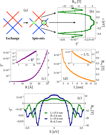
The dependence of the Hall response on the size of the graphene flake is shown in Fig. 4(d), for a fixed radius of nm and an exchange of meV. We see that by increasing the flake size while keeping the skyrmion radius fixed, the Hall signal decreases as , where is the linear size of the triangular transmission region. From these results we infer that the Hall conductance behaves as as a function of the radius and of the linear size of the central island. This scaling reflects the fact that the Hall response is proportional to the probability that the electrons surf over the skyrmion, which is manifestly an increasing function of and a decreasing function of .
By changing both the radius and the device size by a common factor , scales as indicating that the Hall conductance is not scale invariant under simultaneous rescaling of and . Now, since we are considering flakes of the minimum experimentally achievable dimensions proximized with the smallest skyrmions experimentally detected so far (of the order of the nm, whereas observation of skyrmions with radius of up to 100 nm has been reportedYu et al. (2010); Wiesendanger (2016)), the presented scaling argument evidences that our estimates of Hall conductances of the order of - merely set a lower bound for the range of values that this parameter can undertake in actual laboratory measurements. A general example of this non-linear scaling trend is shown in fig. 4(e) where a comparison of two systems with and scaled by a common factor is presented.
We note that most systems in the brink of hosting skyrmion lattices need a non-zero external magnetic flux to drive them into the skyrmionic phase, as they typically exhibit spiral spin phases at zero magnetic field. This implies that an additional non-zero Hall contribution is to be expected from the external field that sums up to the one driven by the skyrmion alone. An effective way to discriminate between the two effects relies on their different symmetry properties. In fact, while the skyrmionic contribution is electron-hole symmetric (as made clear by fig. 4(b)) and changes sign only by switching the sign of either or , the Hall effect induced by the magnetic field is electron-hole asymmetric as holes have opposite charge with respect to electrons and thus respond with an opposite velocity to an applied external magnetic field. It is thus the asymmetry of the overall scattering cross-section that allows to subtract the spurious external contribution and determine the intrinsic skyrmionic one.
IV.2 Effects of disorder
So far we have dealt with a graphene flake perfectly clean. However, some current degradation brought about by defects or impurities in the sample is to be expected. In order to provide a more realistic estimate of the extent to which the Hall responses that our results anticipate are robust with respect to this loss of conductance, we now consider the effect of introducing an amount of scalar disorder in the samples. We do so by averaging over Anderson disorder configurations in each of which we assign a random scalar on-site potential to each atom in the quantum dot and tune the parameter controlling the disorder degree from 0 to a maximum of meV, an upper limit for the energy scale associated with disorder that is consistent with the assumption of Coulomb long-range scatteringWang et al. (2015); Nomura and MacDonald (2007). The clean limit is recovered for .
We employ square leads and compare two disorder configurations with different symmetry: one where the disorder distribution preserves mirror symmetry with respect to the axis and one where the distribution is completely random in the whole sample. A realization of each of these different disorder profiles is shown in fig. 5(a,b). Error bars associated with the standard deviation of the data are shown for completeness.
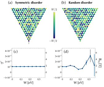
From the resulting curves shown in fig. 5(c,d) we see that symmetric disorder barely affects the Hall response of the problem, as it provokes changes in the normalized transmission imbalance of the order of . On the other side, a randomly distributed disorder that does not respect symmetry affects the conductance more sizeably, yielding variations of the order of . The difference could be explained by noting that in the symmetric case the defects simply act as a fluctuating potential that does not contribute to the asymmetry of the scattering, whereas in the random case an additional transverse conductance driven by the disorder asymmetry rather than by the skyrmion-induced AHE is generated. However, significant alterations of the Hall response only take place at relatively high values of the disorder potential of the order of meV, whereas for weaker and more reasonable disorder strengths the change in the conductance is smaller and comparable to the one obtained in the symmetric configuration. We can therefore safely rely on the results obtained so far for pristine graphene, as the unavoidable presence of a low concentration of defects and noise in the actual samples is not able to turn down the figure of merit of the problem.
V Conclusions
Our results strongly indicate that graphene would be an excellent skyrmion detector at realistic exchange couplings of the order of - meV, exhibiting minimum Hall conductances of the order of - , several orders of magnitude larger than the minimum experimentally detectable conductance of the order of Tzalenchuk et al. (2010); Jeckelmann and Jeanneret (2001). The equivalent magnetic field can easily reach one Tesla for meV , nm and nm. Besides, these values merely set a lower bound estimate for the conductances that are detectable in actual experimental devices where sample dimensions, skyrmion radius and even skyrmion number can be consistently larger than those considered in this work. Our results also show that at weak coupling Schrodinger electrons are less sensitive to the non-trivial magnetic ordering and respond with a conductance that is some orders of magnitude smaller than that displayed by Dirac electrons. Finally, we proved that scalar disorder does not affect the transverse conductance in a dramatic manner.
In conclusion, we suggest that graphene might be exploited as a non-invasive probe to readout the presence of an individual skyrmion in a material underneath. The underlying physical principle is the enhanced anomalous Hall effect due to the interaction of Dirac graphene fermions with non-coplanar spin textures. Our work establishes the principles of hybrid devices combining graphene Hall probes and insulating skyrmionic materialsSeki et al. (2012); Langner et al. (2014); Zhang et al. (2016).
Acknowledgements.
The authors acknowledge financial support by Marie-Curie-ITN 607904-SPINOGRAPH. JFR acknowledges financial supported by MEC-Spain (FIS2013-47328-C2-2-P and MAT2016-78625-C2) and Generalitat Valenciana (ACOMP/2010/070), Prometeo, by ERDF funds through the Portuguese Operational Program for Competitiveness and Internationalization COMPETE 2020, and National Funds through FCT- The Portuguese Foundation for Science and Technology, under the project PTDC/FIS-NAN/4662/2014 (016656). This work has been financially supported in part by FEDER funds. JLL and FF thank the hospitality of the Departamento de Fisica Aplicada at the Universidad de Alicante. We are grateful to F. Guinea and P. San-Jose for useful discussions.Appendix: Determination of
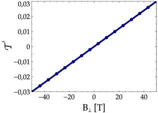
In order to determine the equivalent magnetic field , we have performed a calculation of the transmission imbalance of a three-terminal triangular device where a perpendicular magnetic field is applied to the transmission region. To include such field, we retain only the hopping term of eq. 12 where we perform the standard Peierls substitution such that
| (19) |
By calculating the transmission imbalance between left and right lead, one gets a linear relation as shown in fig. 6. The linear relation between and , in the absence of a skyrmion, permit to assign an equivalent field to characterize the transmission imbalance calculated in the presence of a skyrmion at .
References
- Roszler et al. (2006) U. K. Roszler, A. N. Bogdanov, and C. Pfleiderer, Nature 442 (2006).
- Duine (2013) R. Duine, Nat Nano 8, 800 (2013).
- Rosch (2017) A. Rosch, Nat Nano 12, 103 (2017).
- Dupé et al. (2016) B. Dupé, G. Bihlmayer, M. Böttcher, S. Blügel, and S. Heinze, Nature Communications 7, 11779 EP (2016).
- Edi (2013) Nat Nano 8, 883 (2013).
- Mühlbauer et al. (2009) S. Mühlbauer, B. Binz, F. Jonietz, C. Pfleiderer, A. Rosch, A. Neubauer, R. Georgii, and P. Böni, Science 323, 915 (2009).
- Münzer et al. (2010) W. Münzer, A. Neubauer, T. Adams, S. Mühlbauer, C. Franz, F. Jonietz, R. Georgii, P. Böni, B. Pedersen, M. Schmidt, A. Rosch, and C. Pfleiderer, Phys. Rev. B 81, 041203 (2010).
- Yu et al. (2012) X. Yu, N. Kanazawa, W. Zhang, T. Nagai, T. Hara, K. Kimoto, Y. Matsui, Y. Onose, and Y. Tokura, Nature communications 3, 988 (2012).
- Tokunaga et al. (2015) Y. Tokunaga, X. Yu, J. White, H. M. Rønnow, D. Morikawa, Y. Taguchi, and Y. Tokura, Nature communications 6 (2015).
- Seki et al. (2012) S. Seki, X. Yu, S. Ishiwata, and Y. Tokura, Science 336, 198 (2012).
- Langner et al. (2014) M. C. Langner, S. Roy, S. K. Mishra, J. C. T. Lee, X. W. Shi, M. A. Hossain, Y.-D. Chuang, S. Seki, Y. Tokura, S. D. Kevan, and R. W. Schoenlein, Phys. Rev. Lett. 112, 167202 (2014).
- Zhang et al. (2016) S. Zhang, A. Bauer, H. Berger, C. Pfleiderer, G. van der Laan, and T. Hesjedal, Applied Physics Letters 109, 192406 (2016).
- Heinze et al. (2011) S. Heinze, K. von Bergmann, M. Menzel, J. Brede, A. Kubetzka, R. Wiesendanger, G. Bihlmayer, and S. Blugel, Nat Phys 7, 713 (2011).
- Romming et al. (2015) N. Romming, A. Kubetzka, C. Hanneken, K. von Bergmann, and R. Wiesendanger, Phys. Rev. Lett. 114, 177203 (2015).
- Yu et al. (2010) X. Z. Yu, Y. Onose, N. Kanazawa, J. H. Park, J. H. Han, Y. Matsui, N. Nagaosa, and Y. Tokura, Nature 465, 901 (2010).
- Pfleiderer (2011) C. Pfleiderer, Nat Phys 7, 673 (2011).
- Dovzhenko et al. (2016) Y. Dovzhenko, F. Casola, S. Schlotter, T. X. Zhou, F. Büttner, R. L. Walsworth, G. S. Beach, and A. Yacoby, arXiv preprint arXiv:1611.00673 (2016).
- Parkin et al. (2008) S. S. Parkin, M. Hayashi, and L. Thomas, Science 320, 190 (2008).
- Jonietz et al. (2010) F. Jonietz, S. Mühlbauer, C. Pfleiderer, A. Neubauer, W. Münzer, A. Bauer, T. Adams, R. Georgii, P. Böni, R. A. Duine, K. Everschor, M. Garst, and A. Rosch, Science 330, 1648 (2010).
- Nagaosa and Tokura (2013) N. Nagaosa and Y. Tokura, Nat Nano 8, 899 (2013).
- Hamamoto et al. (2015) K. Hamamoto, M. Ezawa, and N. Nagaosa, Physical Review B 92, 115417 (2015).
- Yin et al. (2015) G. Yin, Y. Liu, Y. Barlas, J. Zang, and R. K. Lake, Physical Review B 92, 024411 (2015).
- Lado and Fernández-Rossier (2015) J. L. Lado and J. Fernández-Rossier, Phys. Rev. B 92, 115433 (2015).
- Nagaosa et al. (2010) N. Nagaosa, J. Sinova, S. Onoda, A. H. MacDonald, and N. P. Ong, Reviews of Modern Physics 82, 1539 (2010).
- Brede et al. (2014) J. Brede, N. Atodiresei, V. Caciuc, M. Bazarnik, A. Al-Zubi, S. Blügel, and R. Wiesendanger, Nature nanotechnology 9, 1018 (2014).
- Banszerus et al. (2016) L. Banszerus, M. Schmitz, S. Engels, M. Goldsche, K. Watanabe, T. Taniguchi, B. Beschoten, and C. Stampfer, Nano letters 16, 1387 (2016).
- Freitag et al. (2016) N. M. Freitag, L. A. Chizhova, P. Nemes-Incze, C. R. Woods, R. V. Gorbachev, Y. Cao, A. K. Geim, K. S. Novoselov, J. Burgdorfer, F. Libisch, et al., Nano Letters 16, 5798 (2016).
- Shalom et al. (2016) M. B. Shalom, M. Zhu, V. Falko, A. Mishchenko, A. Kretinin, K. Novoselov, C. Woods, K. Watanabe, T. Taniguchi, A. Geim, et al., Nature Physics 12, 318 (2016).
- Candini et al. (2011a) A. Candini, C. Alvino, W. Wernsdorfer, and M. Affronte, Phys. Rev. B 83, 121401 (2011a).
- Candini et al. (2011b) A. Candini, S. Klyatskaya, M. Ruben, W. Wernsdorfer, and M. Affronte, Nano Letters, Nano Letters 11, 2634 (2011b).
- González et al. (2013) J. W. González, F. Delgado, and J. Fernández-Rossier, Phys. Rev. B 87, 085433 (2013).
- Qiao et al. (2010) Z. Qiao, S. A. Yang, W. Feng, W.-K. Tse, J. Ding, Y. Yao, J. Wang, and Q. Niu, Phys. Rev. B 82, 161414 (2010).
- Šljivančanin et al. (1997) Ž. V. Šljivančanin, Z. S. Popović, and F. R. Vukajlović, Physical Review B 56, 4432 (1997).
- Castro Neto et al. (2009) A. H. Castro Neto, F. Guinea, N. M. R. Peres, K. S. Novoselov, and A. K. Geim, Reviews of Modern Physics 81, 109 (2009).
- Landauer (1957) R. Landauer, IBM Journal of Research and Development, IBM Journal of Research and Development 1, 223 (1957).
- Sancho et al. (1985) M. L. Sancho, J. L. Sancho, J. L. Sancho, and J. Rubio, Journal of Physics F: Metal Physics 15, 851 (1985).
- Wei et al. (2016) P. Wei, S. Lee, F. Lemaitre, L. Pinel, D. Cutaia, W. Cha, F. Katmis, Y. Zhu, D. Heiman, J. Hone, et al., Nature materials (2016).
- Yang et al. (2013) H. X. Yang, A. Hallal, D. Terrade, X. Waintal, S. Roche, and M. Chshiev, Phys. Rev. Lett. 110, 046603 (2013).
- Qiao et al. (2014) Z. Qiao, W. Ren, H. Chen, L. Bellaiche, Z. Zhang, A. H. MacDonald, and Q. Niu, Physical Review Letters 112, 116404 (2014).
- Okubo et al. (2012) T. Okubo, S. Chung, and H. Kawamura, Physical Review Letters 108, 017206 (2012).
- Wiesendanger (2016) R. Wiesendanger, Nature Reviews Materials 1, 16044 EP (2016).
- Wang et al. (2015) Z. Wang, C. Tang, R. Sachs, Y. Barlas, and J. Shi, Phys. Rev. Lett. 114, 016603 (2015).
- Nomura and MacDonald (2007) K. Nomura and A. H. MacDonald, Physical Review Letters 98, 076602 (2007).
- Tzalenchuk et al. (2010) A. Tzalenchuk, S. Lara-Avila, A. Kalaboukhov, S. Paolillo, M. Syväjärvi, R. Yakimova, O. Kazakova, T. Janssen, V. Fal’Ko, and S. Kubatkin, Nature nanotechnology 5, 186 (2010).
- Jeckelmann and Jeanneret (2001) B. Jeckelmann and B. Jeanneret, Reports on Progress in Physics 64, 1603 (2001).