A new method for measuring excess carrier lifetime in bulk silicon:
Photoexcited muon spin spectroscopy
Abstract
We have measured the optically injected excess carrier lifetime in silicon using photoexcited muon spin spectroscopy. Positive muons implanted deep in a wafer can interact with the excess carriers and directly probe the bulk carrier lifetime whilst minimizing the effect from surface recombination. The method is based on the relaxation rate of muon spin asymmetry, which depends on the excess carrier concentration. The underlying microscopic mechanism has been understood by simulating the four-state muonium model in Si under illumination. We apply the technique to different injection levels and temperatures, and demonstrate its ability for injection- and temperature-dependent lifetime spectroscopy.
Excess carrier lifetime in semiconductors is an extremely sensitive probe of recombination active defect density Schroder ; ReinBook . In the case of silicon, a lifetime spectroscopy can probe as low as 1010 cm-3, corresponding to the carrier lifetime in the order of 10 ms. Therefore the lifetime measurements have been utilized to test a quality of Si wafers in various areas, and especially appreciated in photovoltaic applications where the carrier lifetime is a key parameter for the excess carriers to successfully diffuse across the p-n junction in solar cells. The microchip industries have also found its use as a cleanliness monitor in the chip manufacturing processes. It is now widely accepted that there are three main mechanisms that cause the electron-hole pair (EHP) recombination in semiconductors: 1) Shockley-Read-Hall (SRH) recombination (characterized by its lifetime ), 2) Auger recombination (), and 3) radiative recombination () Schroder ; ReinBook . The bulk recombination lifetime is then given by a relation,
| (1) |
Among those mechanisms, the SRH recombination is a multiphonon process mediated by deep-level defect centers, and dominates in low-level carrier injections, whilst the Auger recombination plays a key role in high-level injections. The radiative recombination is usually negligible in bulk Si due to the indirect band structure.
Although gives a good indication of the level, it alone cannot determine explicitly — it is always necessary to assume the defect type, which is characterized by its energy level and capture cross section for electrons and holes. Deep level transient spectroscopy (DLTS) is therefore commonly utilized to investigate the defect centers Schroder ; ReinBook ; Lang . However Rein et al. ReinBook ; Rein proposed that injection- and temperature-dependent lifetime spectroscopy (IDLS and TDLS) could provide a direct identification of the defect types. The techniques have been demonstrated for Si samples with intentionally introduced metal impurities Rein ; Rein2 .
To measure the carrier lifetime, there are several traditional and novel methods, such as the photoconductance decay (PCD) and photoluminescence decay measurements. Induction-coupled PCD and its varieties are becoming more popular by virtue of their contactless and non-destructive measurement Schroder ; ReinBook ; Cuevas . These techniques measure, by their nature, the effective lifetime of injected carriers, given by . The second term represents a contribution from the surface lifetime which strongly depends on how the wafer surface has been conditioned. It is therefore necessary to extract by 1) treating the surface to make asymptote either 0 (e.g. sandblasting) or (e.g. passivation), or 2) measuring the same samples with different thicknesses and extrapolating the observed lifetimes for . Although these methods are established and widely used, there are few experimental techniques to directly measure , minimizing uncertainties associated with the surface recombination. Those techniques can be important not only in the semiconductor/photovoltaic material engineering, but also in fundamental understanding of the EHP recombination mechanisms.
In this letter we demonstrate a use of positively charged (anti)muon as a contactless probe of in Si. Spin-polarized with an energy of 4 MeV (“surface” muons) are generated in a proton accelerator facility and implanted in bulk materials with the distribution thermalizing over several hundred m. In a case of single crystal Si, the implantation depth can be as deep as 700 m, where the surface effect is negligibly small in most cases. Our recent upgrade of the HiFi muon spectrometer at the ISIS pulsed neutron and muon source in the UK enables us to photoexcite samples with a high-energy laser pulse Yokoyama ; YokoyamaPS ; Wang . A pulsed muon source is useful for time-differential studies, as well as for achieving a large stimulation by virtue of the high-intensity light source. The sample temperature can be varied in a wide range using cryostats and hot stages available in the HiFi experimental suite Yokoyama ; Lord . Combining these capabilities, muon spin spectroscopy (collectively known as SR, corresponding to muon spin relaxation/rotation/resonance) can not only measure the excess carrier lifetime but also investigate its injection and temperature dependence. The muons are an extremely dilute impurity (105 cm-3) and although the muon centers cause recombination, they should have a negligible effect on the bulk carrier lifetime compared to the other impurities present.
Upon implantation, muons decay with a lifetime of 2.2 s and emit positrons preferentially in the muon spin direction, which is then subsequently detected. The obtained time spectrum for muon spin asymmetry carries information on the muon state and its interaction with local atomic/electronic environment Blundell ; Nuccio . The SR technique has been applied to many semiconductor systems, especially to single crystal Si Patterson ; CoxRev . There have been several SR studies on illuminated Si wafers, which report a large photoinduced change in the SR time spectrum KadonoPRL ; KadonoPRB03 ; Fan ; ChowProc .
In semiconductors, an implanted can capture an electron to form a muonium atom (Mu = + + -), a radioisotope of hydrogen. As with H, Mu can exist in three charge states in semiconductors: Mu0, Mu+, and Mu-. In addition, in the case of Si, there are two distinct lattice sites for Mu to occupy: the bond-center site (MuBC) and the interstitial tetrahedral site (MuT). The charge state and lattice site depend on the formation energy determined by the dopant type, concentration, and temperature. For instance, the initial muon asymmetry in intrinsic Si in room temperature (RT) consists of nearly equal amount of Mu and Mu component. The diamagnetic Mu fraction decreases monotonically as decreasing temperature from 250 K down to 200 K. This behavior is attributed to slowing down of the thermally activated ionization of Mu into Mu centers. Therefore, almost the same amount of Mu and Mu can be found in low temperatures, such as T = 77 K Patterson ; CoxRev . When light illuminates a Si sample, injected excess carriers start interacting with the Mu centers in a complex mechanism including spin exchange interaction, cyclic charge exchange reaction, and site change reaction CoxRev ; KadonoPRL ; KadonoPRB03 ; Fan ; ChowProc ; Yokoyama . These interactions result in a spin relaxation of the bound electron in Mu, which then depolarizes the spin via the hyperfine (HF) interaction. Since the relaxation rate of electron spin is proportional to the excess carrier density , the muon spin relaxation rate is sensitive to , and can be used to measure its dynamics. However this assumption is true only in the low rate regime (i.e. relaxation rate of electron spin HF frequency), and the microscopic exchange mechanism is discussed later in this letter.
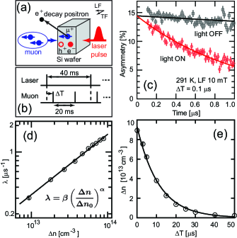
Our experiment has been carried out on a 500-m thick intrinsic single crystal Si wafer (n-type, R 1000 cm, both sides polished) with 111 axis perpendicular to the surface. As shown in Fig. 1(a), one side is facing the incoming pump light, whereas the other side faces the muon beam. Details of the experimental setup, including the sample environment, are explained elsewhere Yokoyama . The distribution of stopped muon is centered in the wafer by adjusting the number of aluminum foil degraders, with its FWHM estimated to be 130 m by a Monte Carlo simulation. Monochromatic 1064-nm laser light injects excess carriers almost uniformly throughout the sample by virtue of its low absorption in Si. The excess carrier density has been calculated based on an absorption coefficient (293 K) = 14.32 cm-1 measured in RT, and (77 K) = 2.37 cm-1 taken from the literature Macfarlane . Because of the long absorption lengths compared with the wafer thickness, we assume that the central density represents for the entire sample. The illuminated area on the sample is 9.6 cm2 and covers the entire area of the muon beam. With these geometries and the calculated carrier diffusion lengths ranging 100 – 200 m, the surface effect is negligible in the obtained lifetime spectra. Fig. 1(b) illustrates the pulse timing, in which muon pulses arrive at the sample at after laser pulses. Since the repetition rate of laser and muon are 25 and (pseudo-)50 Hz respectively Yokoyama , the muon data are sorted and binned to “light ON” and “light OFF” spectra, and averaged for statistics, assuming that the photoinduced change is already over after 20 ms. In the optical setup, two attenuator assemblies and calibrated neutral density filters are used to control the pump laser energy accurately for a wide range of carrier injection.
Fig. 1(c) shows representative light OFF/ON SR time spectra for Si in 291 K under LF 10 mT. The initially formed Mu makes a rapid transition to Mu, which is then quickly ionized to Mu. Thus the light OFF time spectrum is constituted of the diamagnetic Mu center, which shows a very small relaxation because the Zeeman interaction “locks” them along the field direction. Upon illumination at = 0.1 s generating = , the muon spin asymmetry shows a significant relaxation. Based on the timescale of excess carrier recombination and the microscopic mechanism as described below, we use the first 1 s in the spectrum as the fitting range assuming that is constant in this period. The light OFF spectrum is fitted to with and as fitting parameters. Then the light ON spectrum is fitted to the same functional form but with fixed , and a free relaxation rate . Because this relaxation rate arises as a consequence of the Mu-photocarrier interaction, we consider that is a relaxation rate specific for this . is then measured as a function of with fixed = 0.1 . The data is then fitted to a power law indicated in Fig. 1(d) with and as fit parameters. From the obtained function, it is now possible to calculate from a measured . We can therefore measure as a function of and determine the carrier lifetime. Fig. 1(e) shows the obtained decay curve and a fit to with and as fit parameters.
Based on the obtained decay constant, , which is considered to be equivalent to , let us calculate assuming that the defect type is interstitial iron (Fei), a common deep-level defect center in Si wafers. Because of the moderate injection level, the SRH process is the predominant recombination mechanism i.e. . The SRH model Schroder ; ReinBook enables us to calculate based on the recombination parameters of Fei in Si in RT: , where is energy level of the Fei defect center measured from the valence band maximum, and and are its capture cross section for electrons and holes respectively Macdonald . A straightforward calculation gives for this wafer.
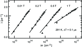
This lifetime spectroscopy utilizing the spin relaxation rate as a probe of n enables us to investigate in a wide range of injection level, an essential parameter for the IDLS measurement, by changing the magnitude of LF. For example, in LF 10 mT, the fit quality for light ON spectra becomes gradually worse when exceeds because the relaxation rate is too fast (see Fig. 1(d)). On the other hand if is less than , the fit quality is also poor because the relaxation is now too slow. It is however possible to change the “sensitivity” of interaction between the Mu centers and excess carriers by changing the magnitude of LF — this is corresponding to varying the Zeeman interaction of muon spin with respect to the Mu HF interaction Chow . In other words a high field decouples the Mu HF interaction so that the spin is less sensitive to the interaction between Mu centers and injected electrons/holes. Therefore we can tune for the best fit quality depending on the injection levels. As shown in Fig. 2, three more injection levels have been measured for the curve under 0.2, 0.5, and 1.0 T. The decay curve for each field is measured in the same way as Fig. 1(e), and gives = 9.4 0.3, 9.0 1.1, and 9.2 0.8 s for 0.2, 0.5, and 1.0 T respectively. Based on the same argument as the 10 mT data, . The SRH model with the calculated defect density predicts that is the fastest recombination process and dominates up to , which agrees with the obtained lifetimes.
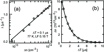
We now apply the method in a low temperature, 77 K, to demonstrate its feasibility for the temperature dependent measurements. Thermally activated transition from the predominant Mu centers, Mu and Mu, is negligibly small in this temperature. Under low LF fields, the SR signal relaxes fast because of the mobile Mu (see below). As we have seen in Fig. 1(c) and (d), sets the minimum usable in the curve. Therefore, for 77 K data, the LF magnitude has been changed to 0.15 T so that is negligibly small (0.0118(3) ), whilst is in the same injection level as Fig. 1(d). Fig. 3(a) and (b) show the obtained and carrier decay curve. The same analysis and fitting method as the 291 K data can be applied and give . This significantly shorter carrier lifetime is associated with an increase of the capture cross section of defect centers. Considering that the sample temperature is too high for the cascade capture process to be predominant Lax , the most likely mechanism is the excitonic Auger recombination HangleiterTheo .
The lifetime measurement in low temperature can also be performed using the precession signal of Mu, which is readily observable under a weak TF. The same procedure is applied to the Mu signal under TF 0.2 mT to measure the curve, and subsequently the lifetime spectrum. The difference here is that the Mu precession in dark is already damped () because of magnetic field inhomogeneity of the instrument and the quantum diffusion of Mu, which interacts with impurities in material Patterson . Therefore the fit function for light ON should have a decay term, , to find the photoinduced rate separately (see Supplemental Material for details of this analysis SM ). The obtained carrier lifetime, , agrees well with the LF measurement (Fig. 3), implying that both methods can observe the same excess carrier recombination. However the LF measurement is considered best suited for IDLS and TDLS measurements because of the ability to tune the field for an interested injection level as seen in Fig. 2, and the applicability for a wide temperature range. The latter advantage is also endorsed by previous photoexcited SR studies on Si, which found a large photoinduced relaxation in the MuBC precession not only in the low temperature range continuously down to several Kelvins Fan but also in the high temperatures up to 550 K ChowProc .
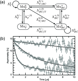
We have so far demonstrated the lifetime measurements based on the empirical observation that can be a useful yardstick of . But what is the underlying microscopic mechanism? To answer this question it is necessary to study the model of Mu dynamics, which was originally used to analyze RF-SR data Kreitzman , and later applied to a photoexcited SR experiment Fan . The four-state model shown in Fig. 4(a) is based on the three-state model used by Fan et al., but has the Mu state in addition, which becomes more important for n 1014 cm-3 Fan . Transition from one Mu state to another is characterized by a transition rate , which can depend on the capture cross section for electron/hole, electron/hole density, activation energy, and prefactor. Because this network is activated upon photocarrier injection, what we observe in the SR spectrum is the dynamics of Mu transition, rather than a signal from static Mu states. To gain the comprehensive picture it is crucial to study a full SR time spectrum, where n stays constant throughout. We therefore ran the same set of experiments as Fig. 1 but using a thicker wafer with a longer carrier lifetime to satisfy this condition (see inset in Fig. 5). Fig. 4(b) shows three representative SR spectra out of eight n’s. We perform a simultaneous fit for the spectra with ’s as global fit parameters, from which ’s are calculated based on the known n. This simulation and fit have been carried out using QUANTUM LordQuantum , a program to solve the time evolution of the muon spin using the density matrix method, running on Mantid Mantid . See Supplemental Material for details of this computation SM . The fit result firstly tells us enhanced rates in and upon carrier injection. Because the rates are much faster than the HF frequencies in Mu (92 MHz), the muon spin is hardly depolarized in this cycling transition. Secondly a high n opens two channels, which “leaks” the MuBC states to the others. Some of Mu escape to the Mu state via , where the HF interaction (2 GHz) depolarizes the muon spin — this is the fast relaxing part in Fig. 4(b). Others are converted from Mu to Mu via , which is an inert, less interactive Mu center with carriers — and this is the subsequent slow relaxing tail. As n decreases, these channels become narrower, resulting in isolated MuBC. Slow decay in the lowest n in Fig. 4(b) is thus attributed to causing the relaxation during the fleeting window when the cycling MuBC state is in Mu. Based on these observations we conclude that the first 1 s window used in the lifetime measurement is corresponding to fitting primarily the fast Mu relaxation. Tuning the Mu sensitivity in a higher field (Fig. 2) is equivalent to decoupling the HF interaction in Mu. The sub-linear dependence of on n (i.e. 0.7) stems from the transition path for Mu leading to Mu.
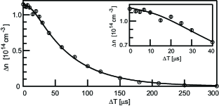
Finally Fig. 5 shows the carrier decay curve for the long-lifetime wafer. The curve is apparently different from the single exponential decay, but has a shoulder around 20 s, where the fast surface recombination driven by carrier diffusion comes into play. This lifetime spectrum can be modelled with a simple 1-dimensional diffusion equation for , , where is the carrier diffusion constant. Because the wafer surfaces have been lapped and chemically polished, the surface velocity should be 104 cm/s. We therefore assume a boundary condition on the surfaces, , and analytically solve the equation with an initial condition, . With , , and as fit parameters, the solid line in Fig. 5 shows a fit to . The obtained = (2 1) 102 s agrees with s, which has been measured by the wafer manufacturer (PI-KEM Ltd.) using the standard PCD method.
In conclusion, excess carrier lifetime in Si has been measured using photoexcited muon spin spectroscopy. This novel technique enables us to measure directly by virtue of the implanted muons as a bulk probe, and can access a wider range of recombination lifetime (from 50 ns to 20 ms), injection level, and temperature. The four-state model has been utilized to explain the underlying microscopic mechanism about how exhibits the dependence on n. The high time resolution, much shorter than the , is possible only with a short-pulsed laser, and distinguishes this study from the previous experiments using lamps. The precisely controlled n is achievable with the collimated beam with narrow linewidth, which gives a predictable uniform absorption profile in the sample. The method can be applied immediately to other semiconductors, such as Ge and GaAs, where interaction of Mu with photoinduced carriers has already been reported FanGe ; YokoyamaGaAs . Its capability on measuring recombination kinetics can be useful in emerging high-efficiency light harvesting materials.
This work has been supported by European Research Council (Proposal No 307593 - MuSES). We wish to acknowledge the assistance of a number of technical and support staff in ISIS and Queen Mary Univ. of London.
References
- (1) D. K. Schroder, Semiconductor Material and Device Characterization, 3rd ed. (John Wiley & Sons, Inc., Hoboken, 2006).
- (2) S. Rein, Lifetime Spectroscopy: A Method of Defect Characterization in Silicon for Photovoltaic Applications (Springer Science & Business Media, 2006).
- (3) D. V. Lang, Journal of Applied Physics 45, 3023 (1974).
- (4) S. Rein, T. Rehrl, W. Warta, and S. W. Glunz, Journal of Applied Physics 91, 2059 (2002).
- (5) S. Rein and S. W. Glunz, Applied Physics Letters 82, 1054 (2003); Journal of Applied Physics 98, 113711 (2005).
- (6) A. Cuevas and D. Macdonald, Solar Energy 76, 255 (2004).
- (7) K. Yokoyama, J. S. Lord, P. Murahari, K. Wang, D. J. Dunstan, S. P. Waller, D. J. McPhail, A. D. Hillier, J. Henson, M. R. Harper, P. Heathcote, and A. J. Drew, Review of Scientific Instruments 87, 125111 (2016).
- (8) K. Yokoyama, P. Murahari, P. Heathcote, L. Nuccio, J. S. Lord, N. A. Morley, and A. J. Drew, Phys. Scr. 88, 68511 (2013).
- (9) K. Wang, P. Murahari, K. Yokoyama, J. S. Lord, F. L. Pratt, J. He, L. Schulz, M. Willis, J. E. Anthony, N. A. Morley, L. Nuccio, A. Misquitta, D. J. Dunstan, K. Shimomura, I. Watanabe, S. Zhang, P. Heathcote, and A. J. Drew, Nat Mater 16, 467 (2017).
- (10) J. S. Lord, I. McKenzie, P. J. Baker, S. J. Blundell, S. P. Cottrell, S. R. Giblin, J. Good, A. D. Hillier, B. H. Holsman, P. J. C. King, T. Lancaster, R. Mitchell, J. B. Nightingale, M. Owczarkowski, S. Poli, F. L. Pratt, N. J. Rhodes, R. Scheuermann, and Z. Salman, Review of Scientific Instruments 82, 73904 (2011).
- (11) S. J. Blundell, Contemporary Physics 40, 175 (1999).
- (12) L. Nuccio, L. Schulz, and A. J. Drew, J. Phys. D: Appl. Phys. 47, 473001 (2014).
- (13) B. D. Patterson, Rev. Mod. Phys. 60, 69 (1988).
- (14) S. F. J. Cox, Rep. Prog. Phys. 72, 116501 (2009).
- (15) R. Kadono, A. Matsushita, R. M. Macrae, K. Nishiyama, and K. Nagamine, Phys. Rev. Lett. 73, 2724 (1994).
- (16) R. Kadono, R. M. Macrae, and K. Nagamine, Phys. Rev. B 68, 245204 (2003).
- (17) See Supplemental Material http://
- (18) I. Fan, K. H. Chow, B. Hitti, R. Scheuermann, W. A. MacFarlane, A. I. Mansour, B. E. Schultz, M. Egilmez, J. Jung, and R. L. Lichti, Phys. Rev. B 77, 35203 (2008).
- (19) K. H. Chow, I. Fan, M. Egilmez, J. Jung, B. Hitti, Physics Procedia 30, 210 (2012).
- (20) G. G. Macfarlane, T. P. McLean, J. E. Quarrington, and V. Roberts, Phys. Rev. 111, 1245 (1958).
- (21) D. Macdonald and L. J. Geerligs, Applied Physics Letters 85, 4061 (2004).
- (22) K. H. Chow, B. Hitti, and R. F. Kiefl, in Semiconductors and Semimetals, edited by M. Stavola (Elsevier, 1998), pp. 137-207.
- (23) M. Lax, Phys. Rev. 119, 1502 (1960).
- (24) A. Hangleiter, Phys. Rev. B 37, 2594 (1988).
- (25) S. R. Kreitzman, B. Hitti, R. L. Lichti, T. L. Estle, and K. H. Chow, Phys. Rev. B 51, 13117 (1995).
- (26) J. S. Lord, Physica B: Condensed Matter 374–375, 472 (2006).
- (27) O. Arnold et al., Nuclear Instruments and Methods in Physics Research Section A: Accelerators, Spectrometers, Detectors and Associated Equipment 764, 156 (2014).
- (28) I. Fan, K. H. Chow, B. Hitti, R. Scheuermann, A. I. Mansour, W. A. MacFarlane, B. E. Schultz, M. Egilmez, J. Jung, Y. G. Celebi, H. N. Bani-Salameh, B. R. Carroll, J. E. Vernon, and R. L. Lichti, Phys. Rev. B 78, 153203 (2008).
- (29) K. Yokoyama, K. Nagamine, K. Shimomura, H. W. K. Tom, R. Kawakami, P. Bakule, Y. Matsuda, K. Ishida, K. Ohishi, F. L. Pratt, I. Shiraki, and E. Torikai, Physics Procedia 30, 231 (2012).