The ARAGORN front-end – An FPGA based implementation of a Time-to-Digital Converter
Abstract
We present the ARAGORN front-end, a cost-optimized, high-density Time-to-Digital Converter platform. Four Xilinx Artix-7 FPGAs implement 384 channels with an average time resolution of 165 ps on a single module. A fifth FPGA acts as data concentrator and generic board master. The front-end features a SFP+ transceiver for data output and an optional multi-channel optical transceiver slot to interconnect with up to seven boards though a star topology. This novel approach makes it possible to read out up to eight boards yielding 3072 input channels via a single optical fiber at a bandwidth of 6.6 Gb/s.
1 Introduction
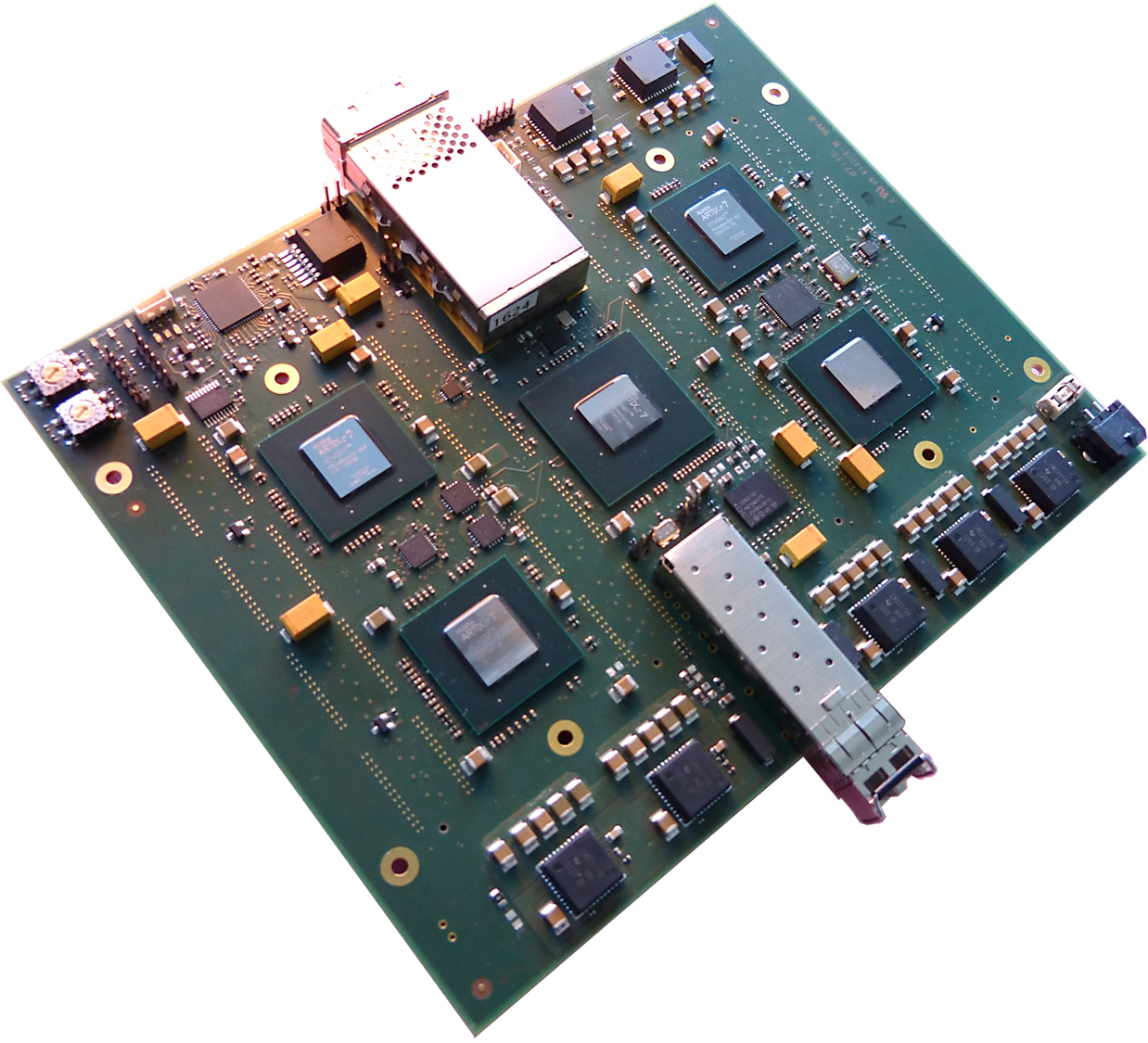
The ARAGORN front-end (figure 1(a)) offers high-performance digital readout capabilities for high-luminosity experimental environments. In order to provide a competitive design that can be operated in widespread applications, the board employs 4 + 1 Xilinx Artix-7 (xc7a200t) FPGAs. Four of these implement a Time-to-Digital Converter (TDC) processing 384 channels on a single module, whereas the fifth FPGA acts as data hub and oversees the communication with auxiliary board components. Implementing the major board functions with low-cost, fully configurable FPGAs ensures long-term usability of this hardware platform, adapting to versatile readout tasks within short development time.
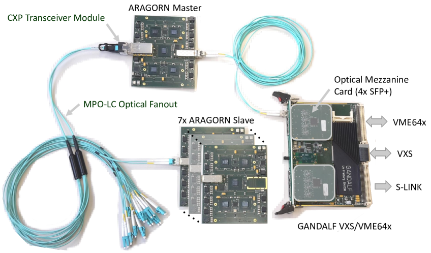
The TDC inputs are linked to four high-speed SMD connectors, providing an interface for extension boards, primarily incorporating the preamplifier and discriminator modules. The acquired data is transferred via source-synchronous serial links to the central FPGA for data output. A highlight of this project is the superior optical readout concept — leveraging both a SFP+ transceiver slot for data output and an optional CXP transceiver socket — to interconnect with up to seven ARAGORN cards as satellites using an optical fanout cable (figure 1(b)). The transceiver modules are in turn attached to the high-speed transceiver tiles of the central FPGA. Consequently, eight boards thus 3072 TDC channels are read out by a single optical fiber connected to the master board that hosts the CXP transceiver. The decisive benefit is that the board layout remains unchanged being operated in master configuration or not. Thanks to its pluggable implementation, the costly CXP module is only required for the master board application, thus strongly reducing the operating expenses.
2 TDC architecture
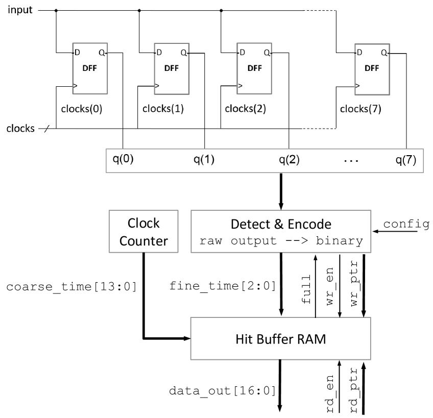
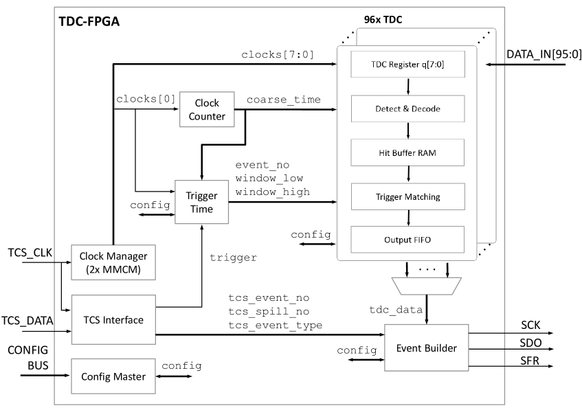
The TDC application implements 96 channels on a single Artix-7 FPGA. The time digitization of the incoming hits is accomplished by sampling the state of the input signal with a quantization step (LSB) of 400 ps. A coarse counter running at sampling clock frequency extends the dynamic range to 16 bits. The result of the fine time measurement is stored together with the coarse time tag in a (2k x 18) integrated memory cell. The entire digitization and readout process is dead time free. Figure 2 shows the block diagram of a TDC channel and the top-level view of the FPGA design to enhance the comprehensibility of the technical description. The benchmarks of the TDC application are summarized in table 1.
| Number of channels | 96 |
|---|---|
| Time bin size (LSB) | 400 ps |
| Sampling clock frequency | 311.04 MHz |
| Average time resolution | 165 ps |
| Differential non-linearity | < 0.3 LSB |
| Integral non-linearity | < 0.3 LSB |
| Input rate | Typical 15 MHz |
| Double hit resolution | 3.2 ns |
| Dynamic range | 16 bits |
| Dead time | None |
2.1 Time digitization principle
Our method connects each input signal to a set of eight edge-triggered flip-flops. The clock inputs of the associated register are driven by a multiphase clock with frequency . The phases are evenly aligned, activating the flip-flops in sequential order with a delay step . The sampling clock is synthesized from an external reference clock input. The ARAGORN front-end was primarily designed to be operated at the COMPASS experiment [2] at CERN. In that case, the sampling clock frequency (cf. table 1) is adjusted to match an integer multiple of the COMPASS reference clock. Two Mixed-Mode Clock Manager (MMCM) primitives inside the FPGA fabric are used to control the phase alignment. The MMCM architecture is based on a phase-locked loop (PLL) and thus automatically maintains a stable characteristic of the converter circuit against supply voltage and ambient temperature variations.
The phase-shifted clocks are distributed on the global clock network of the FPGA, especially designed for low skew and jitter tolerance, to achieve the best possible uniformity of the transfer characteristic. Likewise, any skew present in the input signal to the TDC register contributes to the non-linearity, but automatic routing with similar propagation delay to all net endpoints is not supported. Nonetheless, an interactive routing mode is provided with the Xilinx Vivado GUI to optimize the critical paths. The optimal results obtained for a single TDC register were exported as constraints to lock down the input signal routing in subsequent implementation runs. In order to fix the routing of a net, the placement of the components involved has to be locked as well. A script-based flow was used to apply the same low-skew routing in the implementation of all channels. When the critical portions of the TDC input nets are properly constrained, re-synthesis does not change the transfer characteristic, allowing for design updates without larger effort.
After synchronization, the fine time portion of the measured timestamps is encoded from the register output. The encoding logic can be configured during operation for leading, trailing or even both edge sensitivity. The fine time corresponds to the bin number a hit was found in the register. A coarse counter counting the periods of the sampling clock delivers the coarse time to extend the measurement range. The measurement result combines the fine time information and the coarse counter value. Encoded timestamps are stored in dual-port hit buffers which allow for a dead time free digitization and readout process.
2.2 Trigger matching
In state-of-the-art high-energy physics experiments, pre-processing of digitized data as early as on the front-end boards is essential. In our application, this is achieved with an advanced trigger matching feature. This algorithm selects only such hits from the hit buffers which are time-correlated to the trigger primitives. The time of trigger arrival is digitized with coarse counter precision and a programmable latency time is subtracted to account for the trigger generation and distribution delay. The corrected trigger time defines the lower limit of the acceptance window. The upper limit is determined by a configurable gate time that corresponds to the drift time or time of flight in the detector. Timestamps matching the selective time window are considered to coincide with the trigger event and copied to the output FIFOs. As the trigger matching process might be busy while subsequent triggers arrive, the acceptance window borders are stored in a trigger FIFO for each channel together with an identifier tag.
The search process scans through the hit buffer entries starting from a given memory address until all matching hits are found or the read pointer catches up with the current write address pointer. Finally, the read pointer is relocated to the first entry in the acceptance window as older timestamps are no longer of interest and can be discarded. If for longer periods the trigger matching is idle, the write pointer may catch up with the search start address pointer at some point and assert the buffer full flag. In this case, new hits would be lost. In order to speed up the operation and to prevent buffer overflow conditions, artificial triggers are generated at regular intervals to update the search start address pointer in the hit buffers. Hence another challenge of this algorithm is that coarse counter rollovers invert the comparison operations of the timestamps with the acceptance limits. Thus, the timestamps stored in the hit buffers include an additional rollover bit that is omitted during transfer to the output FIFOs.
2.3 Readout interface
After trigger matching, the corresponding data sets stored in the individual output FIFOs have to be concentrated into a single data stream prior to data output. This is done in a multistage scheme reading the output FIFOs in parallel and buffering the event data for maximum data throughput. In the final stage, the associated event labels are added and the data packages are transfered via a high-speed serial link to the central FPGA. The employed data concentrator modules are highly configurable and easily cascadable to enhance the maintainability of the design.
2.4 Measurement results
The transfer characteristic of the TDC was measured with a statistical code density test. The test signals originated randomly in time from a function generator. Fanout buffer extension boards were employed to cover all inputs of the ARAGORN front-end. If the input signals are uncorrelated with the sampling clock, each time bin of an ideal TDC receives the same number of entries . Assuming a sufficiently large number of measurements , the statistical error can be neglected. Due to the imperfections described in section 2.1, a differential non-linearity (DNL) is obtained in every bin
| (2.1) | ||||
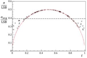
| Figure 3 shows the result for the channel with minimum and maximum DNL. The standard deviation of a measured time interval strongly depends on the fractional part of the quotient [3] | ||||
| (2.2) | ||||
| The average standard deviation is determined by integration of (2.2) within the limits | ||||
| (2.3) | ||||
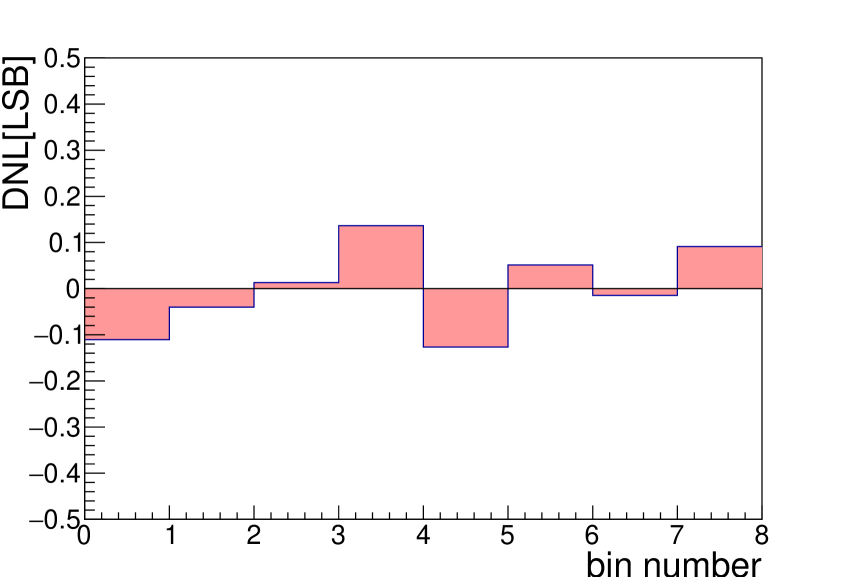
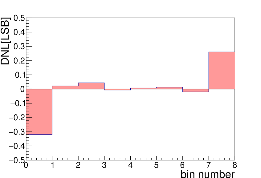
Determining the time resolution of the TDC, we measured constant time intervals between two channels. The calculated standard deviations for all channel of a TDC-FPGA were plotted against the fractional part of the time interval mean divided by LSB. As propagation delays of the input signals on the PCB vary, figure 4 shows a uniform coverage in the interval . The results are in good agreement with the half circle curve corresponding to (2.2) apart from the outer regions where the non-linearity of the transfer characteristic takes effect. The average time resolution of all channels calculated on the basis of this measurement is 165 ps. For the ideal TDC, the time resolution given by (2.3) is 157 ps.
3 Constant latency link
In the uplink direction, the optical network distributes the trigger primitives and the reference clock employed in the TDC application to the front-end boards. This requires that the reference clock recovered in the transceiver tiles maintains a constant phase relationship on all front-ends after a power cycle, reset or a loss of lock. Similarly, the trigger and miscellaneous control signals are expected to approach the receiver nodes with predictable latency, e.g. to simultaneously reset all coarse counter primitives at system startup. These requirements demand for a custom configuration because some features of the GTP high-speed transceivers [4] embedded in the Artix-7 FPGA fabric show latency variations.
Within the scope of high-energy physics experiments, the benefit of synchronous trigger and clock distribution systems based on FPGA transceiver links have been demonstrated and discussed for some time, e.g. in [5]. Besides, our design requires synchronous retransmission of the receiver link data from the master front-end to the slave boards as outlined in section 1. To comply with the strict jitter specifications of the transceiver reference clock source, the ARAGORN front-end features a jitter attenuator. We selected the Texas Instruments LMK04906 device that meets the above prerequisites. The device reliably removes jitter from the recovered clock providing the transceiver tiles and as well the TDC-FPGAs with a clean reference clock.
The GTP transceivers are organized in groups of four, the transceiver quads, sharing two differential external reference clock input pin pairs and two PLLs for the high-speed serial transmitter and as clock seed for the CDR222Clock Data Recovery circuit. Every GTP transmitter/receiver channel consists of a PMA333Physical Medium Attachment and a PCS444Physical Coding Sublayer block. The PMA comprises the serializer/deserializer logic, whereas the PCS handles the parallel data transfer from/to the FPGA fabric. In the receiver PMA, the high-speed CDR clock output is divided to produce the parallel recovered clock. This implies a variable phase offset between these clocks and consequently latency variations in the data path.
The alignment of the incoming data stream to the correct word boundaries is performed internally in the PCS or by user intervention from the FPGA fabric. In the latter, the dedicated RXSLIDE signal is asserted to shift the parallel data by one bit. If the total number of bit shifts required for alignment is even, the bit-slip operation is performed by shifting the phase of the parallel PMA clock only. For odd numbers, a bit shift in the parallel data is involved and the clock phase differs. This is in fact the major reason why a deterministic clock phase cannot be obtained with the standard transceiver configuration.
The solution was to bypass the data alignment and the 8b/10b decoder in the transceiver and implement them inside the FPGA fabric. The parallel data bus of the FPGA interface is 20-bit wide. Our comma detection logic resets the GTP receiver until the alignment sequence (K28.1 + K28.5) is found. This approach completes very quickly as in the link idle state every fourth transmitted symbol is a comma character. The default reset procedure was customized to include the jitter attenuator locked condition. Once the uplink connection is established, the reset of the transmitter channels linked to the slave boards is deasserted. It has become evident that the GTP phase adjust FIFO introduces latency variations in the data path as well. Since the parallel fabric clock and the reference clock originate from redundant outputs of the jitter attenuator, the integrated phase align circuit could be exploited to resolve the phase differences between the PMA clock domains, instead.
4 Embedded design
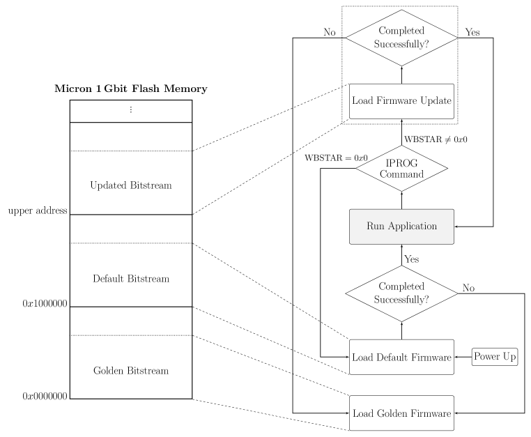
After power-up, the central FPGA retrieves the configuration bitstream from an onboard Flash memory. When the constant latency link is established, the TDC-FPGAs are configured with a bitstream delivered from remote storage. The central FPGA design implements an embedded Microblaze processor to supervise the FPGA configuration, low-speed bus interfaces and in-system Flash programming.
A main objective of applications in environments with limited access like high-energy physics experiments is to maintain remote communication with the readout systems at all times. Figure 5 illustrates our elaborated reconfiguration strategy. If configuration with the default bitstream fails, e.g. due to a CRC error, a fallback sequence is triggered to load a ’golden bitstream’ from the Flash base address. The golden bitstream allows the user to fix up corrupted Flash content and to reconfigure from a given address space. Loading multiple images on the fly is achieved by sending a dedicated command to the Internal Configuration Access Port (ICAPE2) primitive. This feature is highly beneficial for bitstream upgrades and debugging in the field.
5 Conclusion
In conclusion, we present a highly versatile TDC platform with outstanding high-speed optical readout capabilities. This novel approach permits 3072 input channels to be concentrated and read out with a single optical fiber at a bandwidth of 6.6 Gb/s. Another highlight is the superior channel density of a single front-end with a form factor of 140 mm x 172 mm comprising 384 TDC inputs, limited only by connector spacing constraints. Accordingly, we succeeded in the development of a very cost-optimized design. A time resolution of 165 ps for all channels was obtained for the TDC application. The design consumes only 16% of the flip-flop registers and 22% of the look-up tables (LUTs) available in the Artix-7 FPGA. This will allow for future upgrades if applications demand for even higher precision. The digitization bin size could be easily divided in half by doubling the length of the TDC register and engaging the falling edges of the multiphase sampling clock. We furthermore demonstrated the implementation of a constant latency link with the embedded high-speed GTP transceivers. Our approach provides fixed latency data transfer and deterministic phase-synchronous clock distribution even in multi-tiered front-end arrangements. In-system reconfiguration and firmware upgrade strategies have also been developed to entirely oversee and maintain the readout chain remotely. In addition, a system-wide bus interface allows for slow control tasks ranging from register access with command line tools to complete configuration file upload.
Acknowledgments
The authors gratefully acknowledge the support of the local electronic workshop during the front-end design phase. We also appreciate the fruitful discussions with our colleagues from the COMPASS front-end and RICH groups and the endeavours of our collaborators during several testing periods at CERN. This work is supported by the Bundesministerium f r Bildung und Forschung (BMBF) and EU FP7 (Grant Agreement 283286).
References
- [1] F. Herrmann, Development and verification of a high performance electronic readout framework for high energy physics, PhD thesis, Univ. Freiburg, Germany, 2011.
- [2] The COMPASS Collaboration, COMPASS-II Proposal, CERN-SPSC-2010-014, SPSC-P-340, 2010.
- [3] J. Kalisz, Review of methods for time interval measurements with picosecond resolution, Metrologia 41 (2004) 17.
- [4] Xilinx Inc., 7 Series FPGAs GTP Transceivers User Guide, UG482 (2014).
- [5] R. Giordano and A. Aloisio, Fixed-Latency, Multi-Gigabit Serial Links With Xilinx FPGAs, IEEE Transactions on Nuclear Science 58 (2011) 194-201.