Valley dependent anisotropic spin splitting in silicon quantum dots
Abstract
Spin qubits hosted in silicon (Si) quantum dots (QD) are attractive due to their exceptionally long coherence times and compatibility with the silicon transistor platform. To achieve electrical control of spins for qubit scalability, recent experiments have utilized gradient magnetic fields from integrated micro-magnets to produce an extrinsic coupling between spin and charge, thereby electrically driving electron spin resonance (ESR). However, spins in silicon QDs experience a complex interplay between spin, charge, and valley degrees of freedom, influenced by the atomic scale details of the confining interface. Here, we report experimental observation of a valley dependent anisotropic spin splitting in a Si QD with an integrated micro-magnet and an external magnetic field. We show by atomistic calculations that the spin-orbit interaction (SOI), which is often ignored in bulk silicon, plays a major role in the measured anisotropy. Moreover, inhomogeneities such as interface steps strongly affect the spin splittings and their valley dependence. This atomic-scale understanding of the intrinsic and extrinsic factors controlling the valley dependent spin properties is a key requirement for successful manipulation of quantum information in Si QDs.
Introduction
How microscopic electronic spins in solids are affected by the crystal and interfacial symmetries has been a topic of great interest over the past few decades and has found potential applications in spin-based electronics and computation 1; 2; 3; 4; 5; 6; 7. While the coupling between spin and orbital degrees of freedom has been extensively studied, the interplay between spin and the momentum space valley degree of freedom is a topic of recent interest. This spin-valley interaction is observed in the exotic class of newly found two-dimensional materials 8; 9; 10, in carbon nanotubes11 and in silicon 12; 13; 14 —the old friend of the electronics industry. Progress in silicon qubits in the last few years has come with the demonstrations of various types of qubits with exceptionally long coherence times, such as single spin up/down qubits 16; 15, two-electron singlet-triplet qubits 17; 18, three-electron exchange-only 19 and hybrid spin-charge qubits 20 and also hole spin qubits21 realized in Si QDs. The presence of the valley degree of freedom has enabled valley based qubit proposals22 as well, which have potential for noise immunity. To harness the advantages of different qubit schemes, quantum gates for information encoded in different bases are required9; 23; 24. A controlled coherent interaction between multiple degrees of freedom, like valley and spin, might offer a building block for promising hybrid systems.
Although bulk silicon has six-fold degenerate conduction band minima, in quantum wells or dots, electric fields and often in-plane strain in addition to vertical confinement results in only two low lying valley states (labeled as and in Figure 1b) split by an energy gap known as the valley splitting. An interesting interplay between spin and valley degrees of freedom, which gives rise to a valley dependent spin splitting, has been observed in recent experiments15; 25; 26; 27. SOI enables the control of spin resonance frequencies by gate voltage, an effect measured in refs. (16; 25). However, the ESR frequencies and their Stark shifts were found to be different for the two valley states 25. In another work, an inhomogeneous magnetic field, created by integrated micro-magnets in a Si/SiGe quantum dot device, was used to electrically drive ESR15. Magnetic field gradients generated in this way act as an extrinsic spin-orbit coupling and thus can affect the ESR frequency28. Remarkably, although SOI is a fundamental effect arising from the crystalline structure, the ESR frequency differences between the valley states observed in refs. (15) and (25) have different signs when the external fields are oriented in the same direction with respect to the crystal axes. To understand and achieve control over the coupled behavior between spin and valley degrees of freedom, several questions need to be addressed, such as 1) What causes the device-to-device variability?, 2) Can an artificial source of interaction, like inhomogeneous B-field, completely overpower the SOI effects of the intrinsic material?, 3) What knobs and device designs can be utilized to engineer the valley dependent spin splittings?
Results
Here we report experimentally measured anisotropy in the ESR frequencies of the valley states and and their differences , as a function of the direction of the external magnetic field () in a quantum dot formed at a Si/SiGe heterostructure with integrated micro-magnets. At specific angles of the external B-field, we also measure the spin splittings of the two valley states as a function of the B-field magnitude. By performing spin-resolved atomistic tight binding (TB) calculations of the quantum dots confined at ideal versus non-ideal interfaces, we evaluate the contribution of the intrinsic SOI with and without the spatially varying B-fields from the micro-magnets to the spin splittings, thereby relating these quantities to the microscopic nature of the interface and elucidating how spin, orbital and valley degrees of freedom are intertwined in these devices. Finally, by combining all the effects together, we explain the experimental measurements and address the questions raised in the previous paragraph.
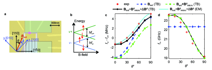
Fig. 1 shows the experimental device, energy levels of interest and measured anisotropic spin splittings compared with the final theoretical results. Details of the device shown in Fig. 1a and the measurement technique of the spin resonance frequency can be found in ref. (15). The external magnetic field is swept from the to crystal orientation. A schematic of the energy level structure is shown in Fig. 1b depicting the and valley states with different spin splittings, where is defined as the ground state. In the experiment, the lowest valley-orbit excitation is well below the next excitation, justifying this four-level schematic in the energy range of interest.
The atomistic calculation with SOI alone (labeled ‘ (TB)’) for a QD at a specifically chosen non-ideal interface and vertical electric field () qualitatively captures the experimental trend of in Fig. 1c, but fails to reproduce the anisotropy of the measured in Fig. 1d in the larger GHz scale. The differences between the experimental data and the SOI-only calculations in both figures arise from the micro-magnets present in the experiment. We can separate the contribution from the micro-magnet into two parts, a homogeneous (spatial average, ) and an inhomogeneous (spatially varying, ) magnetic field. The superscript here indicates that the micro-magnetic fields depend on the direction of (supplementary section S4). The inclusion of the homogeneous part of the micro-magnetic field creates an anisotropy in the total magnetic field (supplementary Fig. S7), which captures the anisotropy of in Fig. 1d very well (, where is the Landé g-factor, is the Bohr magneton and is the Planck constant), but quantitative match with the experimental data in Fig. 1c is not obtained. Next, we also incorporate the inhomogeneous part of the micro-magnetic field, and witness a close quantitative agreement in the anisotropy of , while the anisotropy of is unaffected. This experiment-theory agreement of fig. 1c is achieved for a specific choice of interface condition and , whose influence will be discussed later. Here, we conclude that mainly the intrinsic SOI and the extrinsic inhomogeneous B-field govern the anisotropy of on the MHz scale, while the anisotropy in the total homogeneous magnetic field introduced by the micro-magnet dictates the anisotropy of (and ) on the larger GHz scale.
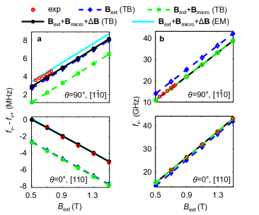
In Fig. 2, we show the measurements of the spin splittings as a function of the magnitude of (), together with the theoretical calculations. The bottom panels show (Fig. 2a) and (Fig. 2b) for along (), whereas the top panels correspond to the B-field along (). In Fig. 2b, depends on through , with . The addition of causes a change in and shifts to coincide with the experimental data. The contributions of and SOI are negligible here in the GHz scale.
On the other hand, comparing the calculated from SOI alone (labeled ‘ (TB)’) for the chosen and interface condition, with experimental data, in both the top and bottom panels of Fig. 2a, it is clear that the experimental B-field dependence of (the slope, ) is captured from the effect of intrinsic SOI, except for a shift between the SOI curve and the experimental data (different shift for and ). The addition of alone does not result in the necessary shift to match the experiment. Only after adding can a quantitative match with the experiment be achieved. Again the experiment-theory agreement is conditional on the interface condition and . Moreover, we see that the addition of does not change the dependency on . Therefore, to properly explain the observed experimental behavior, we can ignore neither the SOI, which is responsible for the change in with , nor the inhomogeneous B-field which shifts regardless of .
Discussion
To obtain a quantitative agreement between the experiment and the atomistic TB calculations, simultaneously in the anisotropy (Fig. 1c) and the (Fig. 2a) dependence of , the only knobs we have to adjust are 1. and 2. interfacial geometry i.e. how many atomic steps at the interface lie inside the dot and where they are located relative to the dot center. These adjustments have to be done iteratively since the steps and not only affect the intrinsic SOI but also the influence of the inhomogeneous B-field. It is easy to separate out the contribution of the SOI from the micro-magnet in the dependence of . It will be shown in Figs. 3 and 4 that, the slope, originates from the SOI, while the micro-magnetic field shifts independent of . First we individually match the experimental “slope” from the SOI and the “shift” from the contribution of the micro-magnet for some combinations of the two knobs. Finally both effects together quantitatively match the experiment for MVm-1, and an interface with four evenly spaced monoatomic steps at -24.7 nm, -2.9 nm, 18.7 nm, 40.4 nm from the dot center along the x () direction. This combination also predicts a valley splitting of 34.4 eV in close agreement with the experimental value, given by 29 eV 27. To describe the QD, a 2D simple harmonic (parabolic confinement) potential was used with orbital energy splittings of 0.55 meV and 9.4 meV characterizing the x and y () confinement respectively. As the interface steps are parallel to y direction, the orbital energy splitting along y has negligible effects, but the strong y confinement significantly reduces simulation time.
To further our understanding, we have complemented the atomistic calculations with an effective mass (EM) based analytic model with Rashba and Dresselhaus-like SOI terms [supplementary section S1], as used in earlier works 31; 32; 25; 30. We have also developed an analytic model to capture the effects of the inhomogeneous magnetic field [supplementary section S2]. The contributions of the SOI and on obtained from these models are shown in equations 1 and 2 respectively.
| (1) |
| (2) |
Here, and are the Rashba and Dresselhaus-like coefficients respectively, is the spread of the electron wavefunction along z, and are the intra-valley dipole matrix elements, is the angle of the external magnetic field with respect to the crystal orientation and are the magnetic field gradients along different directions () for a specific angle . It is clear from these expressions that to match the difference in SOI and dipole moment parameters between the valley states are relevant (but not their absolute values). The parameters used to match the experiment are eVm, eVm, nm, nm and nm. These fitting parameters in the EM calculations enable us to obtain an even better match with the experimental data compared to TB in Figs. 1c and 2a (cyan solid lines). Here we want to point out that the accurateness of the numerically calculated micro-magnetic field values depends on our estimation of the dot location. But as we calculate and independently by comparing the measured for [110] and with equation 1(supplementary section S5), any uncertainty in the estimated dot location or the micro-magnetic field values does not effect the extracted SOI parameters.
As shown in Figs. 1 and 2, three physical attributes play a key role in explaining the experimental data, 1) SOI, 2) , and 3) . Each of these contribute to , and only their sum can accurately reproduce the experimental data for a specific interface condition and vertical electric field, the two knobs mentioned in earlier paragraph. In Figs. 3 and 4, we show separately the effects of 1) and 3) respectively. We show how the contributions of SOI and are modulated by the nature of the confining interface (knob 2). The influence of (knob 1) on the effects of SOI and are shown in the supplementary Figs. S3 and S4 respectively. We also show how modifies the total homogeneous B-field in the supplementary Fig. S7.
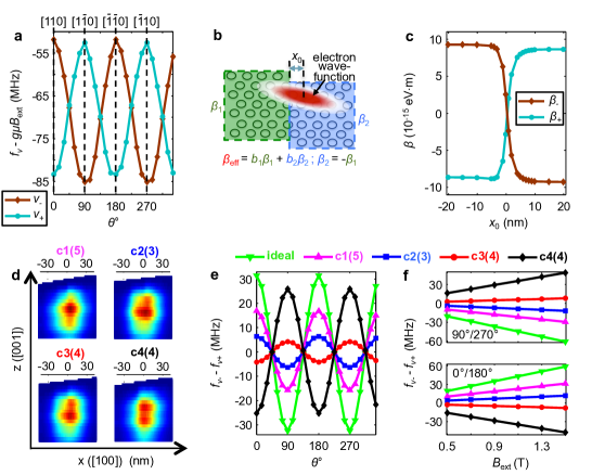
Fig. 3a shows the angular dependence of for a Si QD with a smooth interface calculated from TB. Both and show a 180∘ periodicity but they are 90∘ out of phase. From analytic effective mass study [supplementary equation S11], we understand that the anisotropic contribution from the Dresselhaus-like interaction, caused by interface inversion asymmetry32, results in this angular dependence in . Moreover, the different signs of the Dresselhaus coefficients for the valley states, give rise to a 90∘ phase shift between and . It is important to notice that the change in is in MHz range. So, in GHz scale, like the blue curve (diamond markers) in Fig. 1 d, this change is not visible. However, if we compare and for this ideal interface case, we see at 0∘ and at 90∘, which does not explain the experimentally measured anisotropy. We now discuss the remaining physical parameters needed to obtain a complete understanding of the experiment.
It is well-known that the interface between Si/SiGe or Si/SiO2 has atomic-scale disorder, with monolayer atomic steps being a common form of disorder 33. To understand how such non-ideal interfaces can affect SOI, we first introduce a monolayer atomic step as shown in Fig. 3b and vary the dot position laterally relative to the step, as defined by the variable . By fitting the EM solutions to the TB results [supplementary equation S15], we have extracted the Dresselhaus-like coefficient and plotted it in Fig. 3c as a function of . It is seen that changes sign as the dot moves from the left to the right of the step edge. Both the sign and magnitude of depends on the distribution of the wavefunction between the neighboring regions with one atomic layer shift between them, as shown in fig. 3b. A monoatomic shift of the vertical position of the interface results in a 90∘ rotation of its atomic arrangements about the [001] axis, which results in a sign inversion of the Dresselhaus coefficient of that region32. A dot wavefunction spread over a monoatomic step therefore samples out a weighted average of two s with opposite signs30; 31.
Next, we investigate the anisotropy of (Fig. 3e) with various step configurations shown in Fig. 3d. in Fig. 3e exhibits a 180∘ periodicity, with extrema at the , , , crystal orientations. Both the sign and magnitude of depends on the interface condition. Since decreases when a QD wavefunction is spread over a step edge, the smooth interface case (green curve) has the highest amplitude. Fig. 3f shows that the slope of with changes sign for a 90∘ rotation of and is strongly dependent on the step configuration. The step configuration labeled c3 in Fig. 3d is used to match the experiment in Figs. 1 and 2. So the curves for c3 in both Figs. 3e and 3f correspond to the SOI results of Figs. 1c and 2a. It is key to note here that, as also influences and , shown in supplementary Fig. S3, a different combination of interface steps and can also produce these same SOI results of Figs. 1c and 2a, but might not result in the necessary contribution from micro-magnet to match the experiment. Now the dependence of on the interface condition will cause device-to-device variability, while the dependence on the direction and magnitude of can provide control over the difference in spin splittings. These results thus give us answers to the questions 1 and 3 asked in paragraph 3.
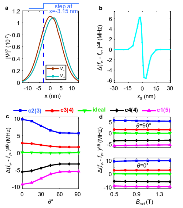
Fig. 4 illustrates how the inhomogeneous magnetic field alone changes (denoted as ). Since vectorially adds to , an anisotropic is seen in Fig. 4c with and without the various step configurations portrayed in Fig. 3d. We also see that in Fig. 4c is negligible for a flat interface, but is significant when interface steps are present. This can be understood from Figs. 4a and 4b, and/or equation 2. Interface steps generate strong valley-orbit hybridization34; 35 causing the valley states to have non-identical wavefunctions, and hence different dipole moments, and/or , as opposed to a flat interface case, which has . Thus the spatially varying magnetic field has a different effect on the two wavefunctions, thereby contributing to the difference in ESR frequencies between the valley states. Fig. 4b shows as a function of the dot location relative to a step edge, (as in Fig. 3b) and illustrates that has the largest contribution to when the step is in the vicinity of the dot. Also, is almost independent of , as shown in Fig. 4d. The curves labeled c3 in both Figs. 4c and 4d correspond to the contribution of in Figs. 1c and 2a. Now also influences , as shown in supplementary Fig. S4. Thus a different combination of interface steps and can also produce these same results of Figs. 1c and 2a, but might not result in the necessary SOI contribution to match the experiment.
A comparison between Figs. 3f and 4d (also between equations 1 and 2) reveals that any dependence of on can only come from the SOI. This indicates that the experimental B-field dependency in Fig. 2a can not be explained without the SOI. So the effect of the SOI cannot be ignored even in the presence of a micro-magnet and this answers question 2 raised in the third paragraph. However, engineering the micro-magnetic field will allow us to engineer the anisotropy of (question 3, paragraph 3). Also, the influence of interface steps will cause additional device-to-device variability (question 1, paragraph 3).
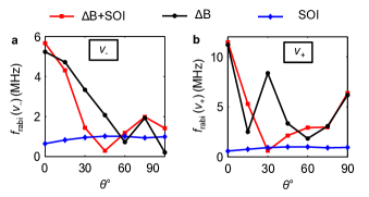
Now the understanding of an enhanced SOI effect compared to bulk, brings forward an important question, whether it is possible to perform electric-dipole spin resonance (EDSR) without the requirement of micro-magnets. Here, we predict that (Fig. 5) for similar driving amplitudes as used here the SOI-only EDSR can offer Rabi frequencies close to 1 MHz, which is around five times smaller than the micro-magnet based EDSR. Moreover, the Rabi frequency of the SOI-EDSR will strongly depend on the interface condition36 (supplementary section S6) and can be difficult to control or improve. On the other hand, with improved design (stronger transverse gradient field) we can gain more advantage of the micro-magnets and drive even faster Rabi oscillations. However, we also predict that, both the SOI and inhomogeneous B-field contribute to the dependence of (supplementary section S3) and make the qubits susceptible to charge noise25. As these two have comparable contribution, both of their effects will add to the charge noise induced dephasing of the spin qubits in the presence of micro-magnets.
The coupled spin and valley behavior observed in this work may in principle enable us to simultaneously use the quantum information stored in both spin and valley degrees of freedom of a single electron. For example, a valley controlled not gate9 can be designed in which the spin basis can be the target qubit, while the valley information can work as a control qubit. If we choose such a direction of the external magnetic field, where the valley states have different spin splittings, an applied microwave pulse in resonance with the spin splitting of , will rotate the spin only if the electron is in . So we get a NOT operation of the spin quantum information controlled by the valley quantum information. Spin transitions conditional to valley degrees of freedom are also shown in ref. (15) and an inter-valley spin transition, which can entangle spin and valley degrees of freedom, is observed in ref. (27).
Conclusion
To conclude, we experimentally observe anisotropic behavior in the electron spin resonance frequencies for different valley states in a Si QD with integrated micro-magnets. We analyze this behavior theoretically and find that intrinsic SOI introduces 180∘ periodicity in the difference in the ESR frequencies between the valley states, but the inhomogeneous B-field of the micro-magnet also modifies this anisotropy. Interfacial non-idealities like steps control both the sign and magnitude of this difference through both SOI and inhomogeneous B-field. We also measure the external magnetic field dependence of the resonance frequencies. We show that the measured magnetic field dependence of the difference in resonance frequencies originates only from the SOI. We conclude that even though the SOI in bulk silicon has been typically ignored as being small, it still plays a major role in determining the valley dependent spin properties in interfacially confined Si QDs. These understandings help us answer the questions raised in paragraph 3, which are crucial for proper operation of various qubit schemes based on silicon quantum dots.
Methods
For the theoretical calculations, we used a large scale atomistic tight binding approach with spin resolved sp3d5s* atomic orbitals with nearest neighbor interactions37. Typical simulation domains comprise of 1.5-2 million atoms to capture realistic sized dots. Spin-orbit interactions are directly included in the Hamiltonian as a matrix element between p-orbitals following the prescription of Chadi 38. The advantage of this approach is that no additional fitting parameters are needed to capture various types of SOI such as Rashba and Dresselhaus SOI in contrast to k.p theory. We introduce monoatomic steps as a source of non-ideality consistent with other works33; 35; 39. The Si interface was modeled with Hydrogen passivation, without using SiGe. This interface model is sufficient to capture the SOI effects of a Si/SiGe interface discussed in refs. (32; 31; 30). We have used the methodology of ref. (29) to model the micro-magnetic fields [supplementary section S4]. Full magnetization of the micro-magnet is assumed. This causes the value of the magnetization of the micro-magnet to be saturated and makes it independent of . However, a change in the direction of changes the magnetization. We include the effect of inhomogeneous magnetic field perturbatively, with the perturbation matrix elements, . Here, and are atomistic wave-functions calculated with homogeneous magnetic field. For further details about the numerical techniques, see NEMO3D reference (37). Method details about the experiment can be found in ref. (15). The dot location in this experiment is different from ref. (15). The device was electrostatically reset by shining light using an LED and all the measurements were done with a new electrostatic environment (a new gate voltage configuration). The quantum dot location is estimated by the offsets of the magnetic field created by the micro-magnets extrapolated from the measurements shown in Fig. 2 and comparing to the simulation results shown in supplementary section S4. We also observed that the Rabi frequencies were different from ref. (15) when applying the same microwave power to the same gate, which qualitatively indicates that the dot location is different.
References
- (1) Datta, S. & Das, B. Electronic analog of the electro-optic modulator. Appl. Phys. Lett. 56, 665(R) (1990).
- (2) Wolf, S. et al. Spintronics: A spin based electronics vision for the future. Science 294, 1488-1495 (2001).
- (3) I. Žutić, Fabian, J. & Das Sarma, S. Spintronics: Fundamentals and applications. Rev. Mod. Phys. 76, 323 (2004).
- (4) Loss, D. & Vincenzo, D. P. Quantum computation with quantum dots. Phys. Rev. A 57, 120 (1998).
- (5) Petta, J. et al. Coherent manipulation of coupled electron spins in semiconductor quantum dots. Science 309, 2180-2184 (2005).
- (6) Koppens, F. et al. Driven coherent oscillations of a single electron spin in a quantum dot. Nature 442, 766-771 (2006).
- (7) Hanson, R., Kouwenhoven, L. P., Petta, J. R., Tarucha, S., Vandersypen & L. M. K. Spins in few electron quantum dots. Rev. Mod. Phys. 79, 1217 (2007).
- (8) Xiao, D., Liu, G.-B. , Feng, W., Xu, X. & Yao, W. Coupled spin and valley physics in monolayers of MoS2 and other group VI dichalcogenides. Phys. Rev. Lett. 108, 196802 (2012).
- (9) Gong, Z. et al. Magnetoelectric effects and valley-controlled spin quantum gates in transition metal dichalcogenide bilayers. Nature Communications 4, 2053 (2013).
- (10) Xu, X., Yao, W., Xiao, D. & Heinz, T. Spins and pseudospins in layered transition metal dichalcogenides. Nature Physics 10, 343–350 (2014).
- (11) Laird, E. A., Pei, F. & Kouwenhoven, L. P. A valley–spin qubit in a carbon nanotube. Nature Nanotech. 8, 565–568 (2013).
- (12) Renard, V. T. et al. Valley polarization assisted spin polarization in two dimensions. Nature Communications 6, 7230 (2015)
- (13) Yang, C. et al. Spin-valley lifetimes in a silicon quantum dot with tunable valley splitting. Nature Communications 4, 2069 (2013).
- (14) Hao, X., Ruskov, R., Xiao, M., Tahan, C. & Jiang, H. Electron spin resonance and spin-valley physics in a silicon double quantum dot. Nature Communications 5, 3860 (2014).
- (15) Kawakami, E. et al. Electrical control of a long-lived spin qubit in a Si/SiGe quantum dot. Nature Nanotechnology 9, 666–670 (2014).
- (16) Veldhorst, M. et al. An addressable quantum dot qubit with fault tolerant control fidelity. Nature Nanotechnology 9, 981–985 (2014).
- (17) Maune, B. M. et al. Coherent singlet-triplet oscillations in a silicon-based double quantum dot. Nature 481, 344–347 (2011).
- (18) Wu, X. et al. Two-axis control of a singlet-triplet qubit with integrated micromagnet. Proc. Natl. Acad. Sci. USA 111, 11938 (2014).
- (19) Eng, K. et al. Isotopically enhanced triple quantum dot qubit. Science Advances 1, no. 4, e1500214 (2015).
- (20) Kim, D. et al. Quantum control and process tomography of a semiconductor quantum dot hybrid qubit. Nature 511, 70-74 (2014).
- (21) Maurand, R. et al. A CMOS silicon spin qubit. Nature Communications 7, 13575 (2016).
- (22) Culcer, D., Sariava, A. L., Koiller, B., Hu, X. & Das Sarma, S. Valley-based noise resistant quantum computation using Si quantum dots. Phys. Rev. Lett. 108, 126804 (2012).
- (23) Rohling, N. & Burkard, G. Universal quantum computing with spin and valley states. New J. Phys. 14, 083008 (2012).
- (24) Rohling, N., Russ, M. & Burkard, G. Hybrid spin and valley quantum computing with singlet-triplet qubits. Phys. Rev. Lett. 113, 176801 (2014).
- (25) Veldhorst, M. et al. Spin-orbit coupling and operation of multivalley spin qubits. Phys. Rev. B 92, 201401(R) (2015).
- (26) Scarlino, P. et al. Second-harmonic coherent driving of a spin qubit in SiGe/Si quantum dot. Phys. Rev. Lett. 115, 106802 (2015).
- (27) Scarlino, P. et al., Dressed photon-orbital states in a quantum dot: Inter-valley spin resonance, Phys. Rev. B 95, 165429 (2017)..
- (28) Tokura, Y., van der Wiel, W. G., Obata, T. & Tarucha, S. Coherent single electron spin control in a slanting Zeeman field. Phys. Rev. Lett. 96, 047202 (2006).
- (29) Goldman, J. R., Ladd, T. D., Yamaguchi, F. & Yamamoto, Y. Magnet designs for a crystal lattice quantum computer. Appl. Phys. A 71, 11 (2000).
- (30) Golub, L. E., & Ivchenko, E. L. Spin splitting in symmetrical SiGe quantum wells. Phys. Rev. B 69, 115333 (2004)
- (31) Nestoklon, M. O., Golub, L. E. & Ivchenko, E. L. Spin and valley-orbit splittings in SiGe/Si heterostructures. Phys. Rev. B 73, 235334 (2006).
- (32) Nestoklon, M. O., Ivchenko, E. L., Jancu, J. -M. & Voisin, P. Electric field effect on electron spin splitting in SiGe/Si quantum wells. Phys. Rev. B 77, 155328 (2008).
- (33) Zandvliet, H. J. W. & Elswijk, H. B. Morphology of monatomic step edges on vicinal Si(001). Phys. Rev. B 48, 14269 (1993).
- (34) Gamble, J. K., Eriksson, M. A., Coppersmith, S. N. & Friesen, M. Disorder-induced valley-orbit hybrid states in Si quantum dots. Phys. Rev. B 88, 035310 (2013).
- (35) Friesen, M., Eriksson, M. A. & Coppersmith, S. N. Magnetic field dependence of valley splitting in realistic Si/SiGe quantum wells, Appl. Phys. Lett. 89, 202106 (2006).
- (36) Huang, W., Veldhorst, M., Zimmerman, N. M., Dzurak, A. S. & Culcer, D. Electrically driven spin qubit based on valley mixing. Phys. Rev. B 95, 075403 (2017).
- (37) Klimeck, G. et al. Atomistic simulation of realistically sized nanodevices using NEMO 3D: Part I—models and benchmarks. IEEE Trans. Electron Dev. 54, 2079–2089 (2007).
- (38) Chadi, D. J. Spin-orbit splitting in crystalline and compositionally disordered semiconductors. Phys. Rev. B 16, 790 (1977).
- (39) Kharche, N., Prada, M., Boykin, T. B. & Klimeck, G. Valley splitting in strained silicon quantum wells modeled with 2° miscuts, step disorder, and alloy disorder. Appl. Phys. Lett. 90, 092109 (2007).
Acknowledgments
This work was supported in part by ARO (W911NF-12-0607); development and maintenance of the growth facilities used for fabricating samples is supported by DOE (DE-FG02-03ER46028). This research utilized NSF-supported shared facilities (MRSEC DMR-1121288) at the University of Wisconsin-Madison. Computational resources on nanoHUB.org, funded by the NSF grant EEC-0228390, were used. M.P.N. acknowledges support from ERC Synergy Grant. R.F. and R.R. acknowledge discussions with R. Ruskov, C. Tahan, and A. Dzurak.
Author contributions statement
R.F. performed the g-factor calculations, explained the underlying physics and developed the theory with guidance from R.R. R.F., R.R., E.K., P.S., and M.P.N. analyzed the simulation results and compared with experimental data in consultation with L.M.K.V., M.F., S.N.C. and M.A.E.. E.K. and P.S. performed the experiment and analyzed the measured data. D.R.W. fabricated the sample. D.E.S. and M.G.L. grew the heterostructure. R.F. and R.R. wrote the manuscript with feedback from all the authors. R.R. and L.M.K.V. initiated the project, and supervised the work with S.N.C, M.F. and M.A.E.
Additional information
The authors declare that they have no competing financial interests.