Quantum-interference transport through surface layers of indium-doped ZnO nanowires
Abstract
We have fabricated indium-doped ZnO (IZO) nanowires (NWs) and carried out four-probe electrical-transport measurements on two individual NWs with geometric diameters of 70 and 90 nm in a wide temperature interval of 1–70 K. The NWs reveal overall charge conduction behavior characteristic of disordered metals. In addition to the dependence of resistance , we have measured the magnetoresistances (MR) in magnetic fields applied either perpendicular or parallel to the NW axis. Our and MR data in different intervals are consistent with the theoretical predictions of the one- (1D), two- (2D) or three-dimensional (3D) weak-localization (WL) and the electron-electron interaction (EEI) effects. In particular, a few dimensionality crossovers in the two effects are observed. These crossover phenomena are consistent with the model of a “core-shell-like structure” in individual IZO NWs, where an outer shell of a thickness ( 15–17 nm) is responsible for the quantum-interference transport. In the WL effect, as the electron dephasing length gradually decreases with increasing from the lowest measurement temperatures, a 1D-to-2D dimensionality crossover takes place around a characteristic temperature where approximately equals , an effective NW diameter which is slightly smaller than the geometric diameter. As further increases, a 2D-to-3D dimensionality crossover occurs around another characteristic temperature where approximately equals (). In the EEI effect, a 2D-to-3D dimensionality crossover takes place when the thermal diffusion length progressively decreases with increasing and approaches . However, a crossover to the 1D EEI effect is not seen because even at = 1 K in our IZO NWs. Furthermore, we explain the various inelastic electron scattering processes which govern . This work demonstrates the complex and rich nature of the charge conduction properties of group-III metal doped ZnO NWs. This work also strongly indicates that the surface-related conduction processes are essential to doped semiconductor nanostructures.
pacs:
73.63.-b, 73.20.Fz, 72.20.-i, 72.80.EyI Introduction
In recent years, nanometer-scale structures have opened up numerous new horizons in both fundamental and applied research Nazarov . Among the various forms of nanoscale structures, nanowires (NWs) provide the unique advantages for facilitating four-probe electrical-transport measurements over a wide range of temperature and in externally applied magnetic fields . In-depth investigations of the rich phenomena and the underlying physics of intrinsic charge and spin conduction processes in single NWs are thus feasible. Indeed, to date, significant advances have been made in studies of metallic Chiquito07 ; LinYH-nano08 ; Chiu-nano09ITO ; Hsu-prb10 ; YangPY-prb12 , magnetic Tatara08 , semiconducting Rueb-prb07 ; Chiu-nano09ZnO ; Tsai-nano10 ; Petersen09 ; Liang10 ; Hau10 ; Xu10 ; Hernandez10 ; Zeng-nanolett12 , and superconducting Arutyunov08 NWs.
Zinc oxide (ZnO) NWs are probably the most extensively studied materials among all kinds of semiconductor NWs, due to their intricate physical properties as well as their widespread potential applications in nanoelectronic and spintronic devices Ozgur05 ; Wang08 . In addition to the initial investigations of natively (unintentionally) doped samples, artificially doped ZnO NWs have attracted much attention. For instance, the n-type doping of Ga and In, among other metal atoms, into ZnO NWs has recently been explored Liu10 ; Ahn07 . The electrical-transport properties of individual In-doped ZnO (hereafter, referred to as IZO) NW JGL09 and NW transistors Xu10 have also been reported. Despite the intense experimental studies in the past years, the electrical conduction mechanisms in the parent ZnO NWs have only been explained recently. Chiu et al. Chiu-nano09ZnO and Tsai et al. Tsai-nano10 have demonstrated that most artificially synthesized ZnO NWs, being essentially independent of the growth method, are moderately highly doped and weakly self-compensated, resulting in a splitting of the impurity band. As a result, the overall charge transport behavior is due to the “split-impurity-band conduction” processes. Furthermore, Chiu et al. Chiu-nano09ZnO and Tsai et al. Tsai-nano10 have shown that many natively doped ZnO NWs, which inherently possess high carrier (electron) concentrations, often lie on the insulating side of, but very close to, the metal-insulator (M-I) transition. Therefore, it is expected that incorporation of a few atomic percent of, e.g., the group-III indium atoms into ZnO NWs may promote the NWs to fall on the metallic side of the M-I transition. (The group-III atoms, Al, Ga, and In, are shallow donors in ZnO Look08 .) Thus, the IZO NWs should reveal electrical conduction properties characteristic to those of disordered conductors. In particular, the quantum-interference weak-localization (WL) and the electron-electron interaction (EEI) effects should be manifest at low temperatures Bergmann84 ; Bergmann10 ; Altshuler85 .
Apart from the interesting low-dimensional electrical-transport properties that could be expected for NW structures, ZnO NWs inherit some complexities, as compared with other NW materials. In particular, the question of whether the surfaces of a ZnO NW are more conducting or less conducting than the bulk has been investigated by several groups. It is now accepted that surface electron accumulation layers, band bending effects, compositional nonstoichiometries, and ambient conditions, etc., can all markedly affect the electrical properties of a surface Schlenker08 ; Allen10 . Recent measurements of resistance and magnetoresistance (MR) by Chiu et al. Chiu-nano09ZnO , Hu et al. Hu09 , and Tsai et al. Tsai-nano10 have revealed that surface conduction is particularly important in those ZnO NWs lying close to the M-I transition. In this context, it would be very interesting to investigate if surface conduction could also be pronounced in IZO NWs which are even more metallic than the natively doped ZnO NWs. Indeed, in this work, we have measured and analyzed the dependence of as well as the dependence of both perpendicular MR and parallel MR in two IZO NWs over a wide interval of 1–70 K. We found a few dimensionality crossovers in the WL and the EEI effects as gradually increases from 1 to 70 K. These results strongly point to dominating roles of the surface-related conduction processes, prompting us to propose a “core-shell-like structure” in individual IZO NWs. This present work demonstrates the complex and rich nature of charge transport processes in ZnO-based NWs. This work also illustrates that quantum-interference transport studies can provide a useful probe for the electron scattering processes in these nanoscale materials. Furthermore, regarding to the materials and technological aspects, we would like to stress that the nature of impurity doping semiconductor nanostructures is intrinsically distinct from doping the bulks. The recent theoretical calculations of Dalpian and Chelikowsky Dalpian06 have shown that dopants would be energetically in favor of segregating to the surfaces rather than distributing uniformly across the radial direction. Their theory provides a strong microscopic support for our experimental observation of a core-shell-like structure in the IZO NWs.
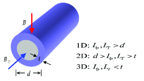
For the convenience of discussion, we first present our model of the core-shell-like structure and summarize the main results of this work. Figure 1 shows a schematic of the core-shell-like structure with a surface conduction layer of a thickness ( 15-17 nm in our IZO NWs). The sizes of the effective NW diameter and the thickness , relative to the electron dephasing length and the thermal diffusion length , determine the observed one-dimensional (1D), two-dimensional (2D), or three-dimensional (3D) WL and EEI effects, as summarized in figure 1. The dephasing length is the characteristic length scale in the single-particle WL effect and the thermal length is the characteristic length scale in the many-body EEI effect, where is the diffusion constant, is the electron dephasing time, is the Planck constant, and is the Boltzmann constant. Table 1 summarizes the various intervals over which different dimensionalities in the WL and the EEI effects are observed in our IZO NWs.
| Nanowire | WL effect | EEI effect | ||||||
|---|---|---|---|---|---|---|---|---|
| 1D | 2D | 3D | 1D | 2D | 3D | |||
| IZO1 | 1–7 K | 7–50 K | 50 K | — | 3–11 K | 14 K | ||
| IZO2 | — | 1–40 K | 40 K | — | — | 3 K |
This paper is organized as follows. In section 2, we discuss our experimental method for the NW synthesis and characterizations as well as the low- four-probe resistance and MR measurements. In sections 3 to 5, we present our experimental results and discussions in great detail. We carry out analyses of the perpendicular MR data and the parallel MR data (section 3) as well as the dependence of (section 4) to illustrate how a conducting outer-layer must exist in single IZO NWs. As a consequence, a few 1D-to-2D and 2D-to-3D dimensionality crossovers in the WL and the EEI effects are observed. In section 5, we identify the underlying electron dephasing processes. Our conclusion is given in section 6.
II Experimental method
Our IZO NWs were synthesized by the laser-assisted chemical vapor deposition (CVD) method, as described previously JGL09 . The scanning electron microscopy (SEM) image in figure 2(a) shows that IZO NWs with diameters ranging roughly from 40 to 100 nm were formed on a tin-coated Si substrate. The high-resolution transmission electron microscopy (HRTEM) image and selected-area electron diffraction pattern in figure 2(b) indicate that In atoms were effectively incorporated into the wurtzite crystal lattice of ZnO and the single crystalline structure with the (0001) growth direction was maintained. Energy-dispersive x-ray (EDX) spectrum displayed in figure 2(c) indicates an In to Zn atomic ratio of approximately 3 at.%, suggesting successful incorporation of In atoms into the ZnO crystal lattice. The NW growth and doping method as well as the structural and composition analyses were previously discussed in reference JGL09, .
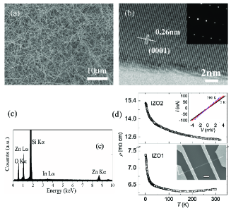
We have fabricated several single IZO NW devices with the four-probe configuration by utilizing the electron-beam lithography technique. The devices reported in this paper were taken from the same batch of NWs. Submicron Cr/Au (10/100 nm) electrodes were made via thermal evaporation deposition. The inset of the lower panel in figure 2(d) shows an SEM image of the IZO1 NW device. The contact resistance between an electrode and the NW is typically a few k at 300 K and 20 k at 4 K. Extensive measurements of the resistances and magnetoresistances have been carried out on two devices. The experimental setup and measurement procedures were similar to those employed in our previous studies of single natively doped ZnO NWs Chiu-nano09ZnO ; Tsai-nano10 and indium tin oxide (ITO) NWs Hsu-prb10 . The and MR curves were measured by utilizing a Keithley K-220 or K-6430 as a current source and a high-impedance (T) Keithley K-2635A or K-6430 as a voltameter. The resistances reported in this work were all measured by scanning the current-voltage (-) curves at various fixed values between 300 and 1 K. The resistance at a given value was then determined from the region around the zero bias voltage, where the - curve was definitely linear, see the inset in the upper panel of figure 2(d). In fact, since our IZO NWs had relatively low resistivities ( 10 m cm) which depended very weakly on in the wide temperature range 1–300 K, the NWs were “metallic-like” and the electron-beam lithographic contacts were already ohmic without any heat treatment. Electron overheating at our lowest measurement temperatures was carefully monitored and largely avoided except that there might be slight heating for those data points taken at = 1 K. This possible slight electron heating at 1 K will not affect any of our discussions and conclusion, except the extracted value of (1 K) might be slightly overestimated (figure 7). Notice that, since we had employed the four-probe configuration, the measured resistances (resistivities) were thus the intrinsic resistances (resistivities) of the individual NWs. The relevant parameters of the two individual IZO NW devices studied in this work are listed in table 2.
| Nanowire | (300 K) | (300 K) | (10 K) | ||||||||
|---|---|---|---|---|---|---|---|---|---|---|---|
| (nm) | (m) | (k) | (m cm) | (m cm) | (cm-3) | (meV) | (nm) | (fs) | (cm2/s) | ||
| IZO1 | 68 | 3.8 | 66.6 | 6.4 | 6.7 | 1.7 | 100 | 2.8 | 7.3 | 3.6 | 2.2 |
| IZO2 | 92 | 1.9 | 35.5 | 12 | 15 | 6.8 | 55 | 2.4 | 8.4 | 2.2 | 1.4 |
III Results and discussion: magnetoresistance in the weak-localization effect
This section is divided into three subsections. In subsection 3.1, we present our estimates of the electronic parameters in our IZO NWs. In subsection 3.2, we present our perpendicular MR data and the observed dimensionality crossovers in the WL effect. In subsection 3.3, we analyze our parallel MR data to further determine and confirm the thickness of the outer conduction shell in single IZO NWs.
III.1 Estimate of nanowire electronic parameters
In order to facilitate quantitative comparison of our and MR data with the WL and the EEI theoretical predictions, we first discuss the estimates of the relevant electronic parameters of our IZO NWs. The carrier concentration of a doped semiconductor NW can not be readily measured, e.g., by using the conventional Hall effect, due to the small transverse dimensions of a single NW. Fortunately, insofar as single-crystalline ZnO materials (films and bulks) are concerned, an empirical relation between the room-temperature resistivity (300 K) and has been comprehensively compiled and reliably established by Ellmer in the figure 4 of reference Ellmer01, . Furthermore, Chiu et al. Chiu-nano09ZnO and Tsai et al. Tsai-nano10 have recently shown that this Ellmer – empirical relation can well be extended to the case of individual single-crystalline ZnO NWs. Therefore, in this study we have applied this empirical relation to evaluate the values in our IZO NWs.
It is worth noting that the values we evaluated (table 2) are in reasonable consistency with that extracted from direct measurements by using the back-gate method JGL09 . For example, in an IZO NW with (4 K) = 2.7 m cm, the back-gate method reported an estimate of 1.2 cm-3. Alternatively, according to the Ellmer – empirical relation Ellmer01 , such a resistivity would infer a value of 8 cm-3. That is, the values estimated according to the two independent methods agree to within a factor of 1.5. Since the critical carrier concentration for the M-I transition in single-crystalline ZnO occurs at 5 cm-3 Chiu-nano09ZnO ; Tsai-nano10 ; Hutson57 , our doped IZO NWs obviously lie on the metallic side of, but close to, the M-I transition. That our NWs lie close to the M-I transition boundary is directly evident in the fact that our measured dependence of is weak, namely, (1 K)/(300 K) 1.2 in both NWs (figure 2(d)). In the IZO1 NW, decreases with reducing between 180 and 300 K, before it increases with further decrease in . The metallic-like behavior results from the incorporation of a few atomic percent of In atoms (donors) into the ZnO NW crystal lattice as well as from the In doping induced oxygen vacancies Liu10 . The notable resistivity rise below 40 K originates from the WL and the EEI effects. Numerically, the (300 K) values of the IZO1 and IZO2 NWs are approximately one order of magnitude lower than those of the natively doped ZnO NWs that we had previously studied Chiu-nano09ZnO ; Tsai-nano10 . Moreover, these (300 K) values are 3 orders of magnitude lower than that in a two-probe individual IZO NW transistor recently fabricated by Xu et al. Xu10 .
In estimating the other charge carrier parameters which are listed in table 2, we have assumed a free-electron model and taken an effective electron mass of in the conduction band Baer67 , where is the free-electron mass. We obtain the electron mobility (300 K) 55 cm2/V s in the IZO1 NW and 75 cm2/V s in the IZO2 NW. These values are slightly lower than that ( 100 cm2/V s) found in natively doped ZnO NWs Chiu-nano09ZnO . Note that our evaluated Fermi energies are 100 and 55 meV in the IZO1 and IZO2 NWs, respectively. These values are larger than the thermal energy at 300 K, and also larger than the major shallow donor level ( 30 meV below the conduction band minimum Chiu-nano09ZnO ; Tsai-nano10 ; LienCC-jap11 ) in the parent ZnO. Therefore, degenerate Fermi-liquid and metallic behavior is to be expected in our NWs. As a consequence, all of our electronic parameters depend only weakly on , as compared with those in typical semiconductor NWs that exhibit, e.g., hopping conduction processes x4 .
III.2 Perpendicular magnetoresistance in the weak-localization effect
In disordered conductors and at low temperatures, the WL and the EEI effects cause pronounced quantum-interference transport phenomena which depend sensitively on and . The WL effect results from the constructive interference between a pair of time-reversal partial electron waves which traverse a closed trajectory in a random potential. The time-reversal symmetry will be readily broken in the presence of a small field Bergmann84 ; Bergmann10 . The low-field MR can provide quantitative information on the various electron dephasing mechanisms, such as the inelastic electron-electron scattering, electron-phonon scattering, spin-orbit scattering, and magnetic spin-spin scattering Lin-jpcm02 . The WL effects in different dimensionalities assume different functional forms of MR Bergmann84 ; Bergmann10 ; Altshuler85 . Therefore, it is of crucial importance to apply the appropriate MR expressions to describe the WL effect in those samples (e.g., NWs and thin films) whose transverse dimensions are comparable to the dephasing length . In such cases, a dimensionality crossover of the WL effect is deemed to occur if the measurement is varied sufficiently widely Mani-prb93 . Moreover, an external applied in the perpendicular or the parallel orientation relative to the current flow can result in distinct MR, because the WL effect is an orbital phenomenon in nature. Similarly, dimensionality crossovers could occur in the EEI effect (section 4).
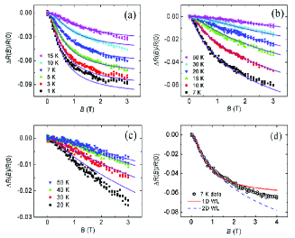
Figures 3(a)–3(d) show the normalized MR, , of the IZO1 NW as a function of perpendicular magnetic field in several regions, as indicated. (The fields were applied perpendicular to the NW axis.) The symbols are the experimental data and the solid curves are the WL theoretical predictions for 1D (figure 3(a)), 2D (figure 3(b)), and 3D (figure 3(c)), respectively. Figure 3(d) shows a plot of the measured perpendicular MR at 7 K together with both the 1D and the 2D WL theoretical predictions, as indicated. We notice that in all figures 3(a)–3(d), the MR data are negative, suggesting that the spin-orbit (s-o) scattering rate is relatively weak compared with the inelastic electron scattering rate at all down to 1 K. In other words, the s-o scattering length is always longer than , where is the s-o scattering time. This observation of a very weak s-o scattering is consistent with the conclusion recently drawn from the WL studies of metallic-like ZnO NWs Chiu-nano09ZnO and ZnO nanoplates Likovich09 ; Andrearczyk05 . Microscopically, the comparatively weak s-o coupling in ZnO is thought to originate from the small energy splitting at the top of the valence band Harmon09 . A doping of 3 at.% of moderately heavy In atoms in this work does not induce any appreciable enhancement of the s-o coupling.
The MR due to the 1D WL effect in the presence of an external applied either perpendicular or parallel to the NW axis is given by Altshuler81 ; Birge03 , in terms of the normalized resistance ,
| (1) | |||||
where is the resistance of a quasi-1D NW of length , and the characteristic time scale represents the dephasing ability of the field. The form of depends on the orientation of relative to the current flow and the shape of the NW Altshuler81 . There are two situations which have been explicitly theoretically calculated. First, for a NW with a square cross section and side in applied perpendicular to the NW axis, , where the magnetic length . Second, for a NW with a circular cross section and diameter in applied parallel to the NW axis, . In practice, both side and diameter can be treated as adjustable parameters, because the effective cross-sectional area responsible for the charge conduction may differ from the geometric cross-sectional area of the given NW under study. In other words, the NW may be inhomogeneous (e.g., due to O vacancies, surface absorption/desoption, variations in compositions, surface states Shalish04 , accumulation layers Grinshpan79 ; Gopel80 , etc.) and the electrical conduction is not through the whole volume of the NW Schlenker08 ; Hu09 .
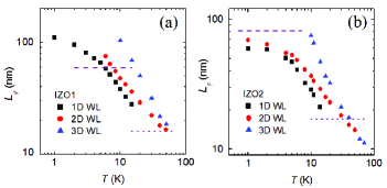
In plotting figure 3(a), we have used equation (1) and rewritten to least-squares fit the measured MR data for 0.5 T, and then generated the theoretical curves for a range up to 3.25 T. (We have treated , and thus , as an adjustable parameter.) Numerically, we obtained -independent (average) values of 59 nm and 140 nm for all the MR curves plotted in figure 3(a). The only -dependent adjustable parameter is , which is plotted in figure 4(a) as a function of . Figure 4(a) shows that (the squares) decreases from 110 nm at 1 K to 28 nm at 15 K. It should be noted that our extracted value becomes shorter than the effective NW diameter as increases to above 7 K. Such a result is not self-consistent and it violates the applicability of equation (1). That is, under such circumstances, one should consider a possible dimensionality crossover to the 3D WL effect at 7 K. A similar observation has recently been pointed out by Hsu et al. Hsu-prb10 in their WL studies of single ITO NWs. In any case, one should be cautious about the validity of the extracted values in this moderately high region.
To examine whether a crossover from the 1D to the 3D WL effect takes place in the IZO1 NW at 7 K, we now compare our MR data with the 3D WL theoretical predictions. The 3D WL MR is given by Lin-jpcm02 ; Fukuyama81 ; Wu-prb94 , in terms of normalized magnetoresistivity ,
| (2) | |||||
where
(= 1.93 in the ZnO material g-factor ) is the electron Lande- factor, is the Bohr magneton, and
Here the characteristic fields are connected with the electron scattering times through the relation , with the subscript stands for (the dephasing field/time), (the inelastic scattering field/time), (the s-o scattering field/time), (the “saturated” scattering field/time as 0 K), and (the elastic scattering field/time). ( will be used in equation (3).) The function is an infinite series which can be approximately expressed as above, which is known to be accurate to be better than 0.1% for all arguments (Ref. Baxter89, ).
Figure 3(c) shows the normalized MR and the least-squares fits to the theoretical predictions of equation (2) at four values between 20 and 50 K. This figure reveals that, as increases to above 20 K, the theoretical curves can reasonably describe the experimental data. The values (triangles) thus extracted are plotted in figure 4(a). We obtain = 50 nm at 20 K and 19 nm at 50 K. Although our measured MR data at 20 K can seemingly be described by the 3D WL theory, we should stress that the agreement between the theory and the experiment is superficial. For instance, the inferred values (triangles) do not extrapolate to those values (squares) inferred from the low- 1D regime. Furthermore, the extracted value would suggest a 3D-to-1D dimensionality crossover taking place at a relatively high 20 K, which is very unlikely. (Recall that the least-squares fits to the 1D MR theory do not lead to self-consistent results for 7 K.) In fact, as we will demonstrate below, the charge carriers in our IZO NWs do not flow through the whole volume of the individual NWs. Instead, there is an outer conduction shell of a thickness in individual IZO NWs (figure 1), which is responsible for our observed quantum-interference electron conduction. Thus, at sufficiently low where , the electrical transport would be 1D with regard to the WL effect. On the other hand, at not too low where , the low-field MR manifests the 2D WL effect. Note that, recently, surface-related electrical conduction processes have also been found in natively doped ZnO NWs which lie on the metallic side of, but close to, the M-I transition Chiu-nano09ZnO .
We now analyze our MR data at 7 K in terms of the 2D WL theory. The MR due to the 2D WL effect in the presence of a perpendicular field is given by Bergmann84 ; Hikami80 ; Lin-prb87a , in terms of normalized sheet resistance ,
| (3) | |||||
where is the digamma function, and was defined below equation (2). is a characteristic field given by . In the least-squares fits of the predictions of equation (3) to our experimental MR data, we have treated the sheet resistance as an adjustable parameter, where the resistance and length are directly measured, and is defined as , with being the geometric diameter of the NW determined via SEM (table 2). Thus, is a fitting parameter. Note that we have approximated the outer conduction shell with a dodecagon in the fits to equation (3) note5 .
Figure 3(b) shows the measured MR and the least-squares fits to equation (3) for the IZO1 NW at several values between 7 and 50 K. This figure clearly indicates that the normalized MR in the low-field regime of 1 T can be well described by the theoretical predictions. Most important, the extracted values (circles) as a function of are plotted in figure 4(a), which lie systematically below those extracted according to the 3D form of equation (2). Inspection of figure 4(a) indicates that the ( 7 K) values inferred from the 2D WL theory, equation (3), closely extrapolate to those ( 7 K) values inferred from the 1D WL theory, equation (1). This observation is meaningful, which strongly suggests that the WL MR effect smoothly crosses over from the 1D regime to the 2D regime as increases to be above 7 K. Indeed, we find that the measured MR data at 7 K and in 1 T can be reasonably well described by both equation (1) and equation (3) (figure 3(d)). Furthermore, it should be noted that, at this particular value, the fitted dephasing length according to equation (3) is (7 K) 64 nm. This is very close to the effective NW diameter ( 59 nm) inferred above from the 1D WL fits. Thus, the physical quantity signifies the characteristic length scale that controls the dimensionality crossover between the 1D () and 2D () WL regimes in the IZO1 NW.
If continues to increase and gradually reduces, one would expect another possible dimensionality crossover from the 2D to the 3D WL effect. In fact, figures 3(b) and 3(c) together indicate that both equation (2) and equation (3) can describe the measured MR data at 50 K and in 1.5 T. The extracted (50 K) values according to both equations approach each other, being 15 nm (figure 4(a)). This result implies that a 2D-to-3D dimensionality crossover takes place around 50 K or slightly higher. In particular, the responsible length scale is 15 nm, which can be identified as the effective thickness of the outer conduction shell. In short, in the IZO1 NW, as monotonically increases and progressively decreases, a 1D-to-2D dimensionality crossover of the WL effect first takes place around 7 K, where (7 K) . As further increases, a 2D-to-3D dimensionality crossover eventually occurs near 50 K, where (50 K) . It should be noted that the existence of a relevant shell thickness of 15 nm is further supported by the EEI effect in the - behavior (figures 6(a) and 6(b)). Thus, continuously fitting the measured MR curves with the 2D WL theory up to 50 K would lead to an inconsistency of .
Apart from the IZO1 NW, we have carried out similar MR measurements on the IZO2 NW. In this second NW, we obtain least-squares fitted average values of 81 nm, 17 nm, and 105 nm. Figure 4(b) shows the values extracted according to the 1D, 2D, and 3D WL MR expressions, as indicated. We find that it definitely needs to apply the 2D WL theory to extract acceptable values of (circles) in this NW. Those values (squares) extracted according to equation (1) are smaller than at all , and thus an interpretation based on the 1D WL effect is not self-consistent. On the other hand, those values (triangles) extracted according to equation (2) are larger than at below 40 K, and thus the 3D WL effect is neither acceptable for 40 K. In other words, our results suggest that the IZO2 NW lies in the 2D regime with regard to the WL effect all the way down to 1 K. There is no crossover to the 1D WL regime because this NW has a larger value while it possesses a shorter , as compared with the IZO1 NW. Physically, the is shorter in the IZO2 NW because this NW is slightly more disordered than the IZO1 NW. In the opposite high region, there is a 2D-to-3D dimensionality crossover taking place around 40 K. At 40 K, the measured MR can be fitted with both equation (2) and equation (3), and the extracted values are similar, being (40 K) 17 nm. It should be noted that this value is relatively close to that ( 15 nm) inferred for the IZO1 NW. These results suggest that this is the typical thickness of the surface conduction shell in our IZO NWs. This characteristic thickness might be a material property of the group-III metal doped ZnO NWs Look08 .
III.3 Two-dimensional parallel magnetoresistance in the weak-localization effect
In this subsection, we intend to provide further evidence for the existence of a surface conduction shell in individual IZO NWs. If there is any quasi-2D structure leading to the 2D WL effect observed in our IZO NWs discussed thus far, measuring the MR in applied parallel to the conduction shell should provide a complementary method for determining the thickness of this conduction shell. The MR due to the 1D WL effect in the presence of a parallel magnetic field, , is already included in equation (1). The MR due to the 2D WL effect in the presence of a parallel is given by ng93 , in terms of normalized sheet resistance ,
| (4) |
where the characteristic lengths , and , with the characteristic fields and being defined below equation (2).
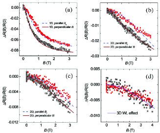
Figures 5(a), 5(b), and 5(c) plot the perpendicular and the parallel MR data of the IZO1 NW at three selected values of 3 K (i.e., the 1D WL regime), 20 K (i.e., the 2D WL regime), and 50 K (i.e., the 2D-to-3D crossover regime), respectively. In each figure, the solid (dashed) curve is the theoretical prediction of the perpendicular (parallel) WL effect. We start with the low- 1D regime. In figure 5(a), the perpendicular MR was first least-squares fitted to equation (1) with the form of as discussed in subsection 3.2, and the solid curve was plotted using the fitted parameters: (3 K) = 81 nm, = 140 nm, and = 59 nm. Then, we substituted this set of parameters into equation (1) but now rewrote the magnetic time in the form of to “generate” the 1D parallel WL MR prediction, without invoking any additional adjustable parameter nor performing any further least-squares fits. This procedure produced the dashed curve which is seen to well describe our measured parallel MR data. Thus, the reliability and validity of our measurement method and data analyses are justified. In fact, we could repeat this practice of using the same set of fitting parameters to describe both the perpendicular and the parallel MR data at a given for all temperatures below 7 K. In figure 5(a), the magnitudes of the perpendicular MR and the parallel MR do not differ markedly, i.e., the MR is not significantly anisotropic, because (3 K) is not considerably longer than in this NW note6 .
At 7 K, our measured perpendicular MR data and the parallel MR data at a given can no longer be simultaneously described by equation (1) with a same set of adjustable parameters. Therefore, we have turned to the 2D forms of the WL theory. In this procedure, if we already know the and values from the analyses of the perpendicular MR data at a given as discussed in subsection 3.2, the conduction shell thickness (which enters ) will be the sole adjustable parameter left in equation (4). Figures 5(b) and 5(c) clearly show that our perpendicular MR data and parallel MR data can be simultaneously described by equation (3) (solid curves) and equation (4) (dashed curves), respectively. From this approach, our extracted value according to equation (4) is 15 nm at both temperatures, firmly confirming the above deduced thickness. In fact, by repeating for several values in the 2D WL regime, we obtain average values of 152 nm for the IZO1 NW and 173 nm for the IZO2 NW (table 3).
Figure 5(d) shows a plot of the perpendicular MR data (open squares) and the parallel MR data (closed circles) as a function of for the IZO2 NW at 70 K. One sees that the perpendicular MR and the parallel MR collapse, explicitly illustrating a 3D behavior. Indeed, at such a high value, must be very short. According to equation (2) (the solid curve), we obtain a least-squares fitted value of (70 K) 11 nm.
Self purification mechanisms preventing doping of semiconductor nanostructures. It should be of crucial importance to point out that, from the Hall effect and secondary-ion mass spectroscopy measurements, Look et al. Look08 have recently inferred that the group-III metal impurities could readily diffuse into the surfaces of any ZnO wafers for a distance of 14 nm. Remarkably, this value independently inferred from entirely distinct physical properties is in close agreement with our extracted value ( 15–17 nm). The underlying physics for this consistency is highly meaningful. Recently, based on energetic arguments, Dalpian and Chelikowsky Dalpian06 have theoretically shown that the “self-purification” mechanisms would perniciously prevent doping of semiconductor nanostructures, causing dopants to segregate to surfaces. This theoretical finding provides a natural explanation for our experimental observation of the “core-shell-like structure” in IZO NWs. This very issue concerning the materials property and the doping behavior of semiconductors at the nanoscale deserves detailed studies before any nanoelectronic devices could be possibly implemented Klamchuen11 .
The absence of Altshuler-Aronov-Spivak (AAS) oscillations. It may be conjectured that a convincing experimental proof of the existence of an outer conduction shell would be an observation of the AAS oscillations at low temperatures AAS82 . AAS had theoretically predicted that the resistance of a weakly disordered cylindrical conductor would oscillate in sweeping fields with a period of . We have checked this predicted phenomenon in this study, but did not observe any signature of such kind of oscillations. This is expected, because a conduction shell of as thick as 15–17 nm in our IZO NWs would strongly suppress the amplitudes of the AAS oscillations, making them more than one order of magnitudes smaller than the parallel MR in the WL effect note7 . Moreover, the AAS oscillations should be further damped due to any inhomogeneities in the conduction shell radius and thickness Aronov87 , which very likely exist in our NWs.
| Sample | ||||||||
|---|---|---|---|---|---|---|---|---|
| K-2/3 s-1 | K-1 s-1 | K-3/2 s-1 | (ps) | (ps) | (nm) | (nm) | (nm) | |
| IZO1 | 1.61010 | 1.11010 | 2.3109 | 67 | 54 | 59 | 159 | 152 |
| IZO2 | — | 9.0109 | 2.2109 | 40 | 47 | 81 | 235 | 173 |
IV Dimensionality crossover in the electron-electron interaction effect
In this section, we concentrate on the data due to the EEI effect to provide further justification for the existence of a core-shell-like structure in IZO NWs. In addition to the WL effect, the many-body EEI effect also results in a resistance rise with decreasing in a weakly disordered conductor Bergmann84 ; Bergmann10 ; Altshuler85 . The EEI effect induced correction in 2D is give by Altshuler85 ; Lin-prb87a , in terms of the normalized sheet resistance ,
| (5) |
where is an arbitrary reference temperature. is an electron screening factor averaged over the Fermi surface, whose value lies approximately between 0 and 1 Altshuler85 ; F-value . The EEI effect induced correction in 3D is give by Altshuler85 ; Lin-prb93 , in terms of the normalized resistivity ,
| (6) |
In the comparison of the theoretical prediction of either equation (5) or equation (6) with experiment, is the only adjustable parameter. The characteristic length scale controlling the sample dimensionality in the EEI effect is the thermal diffusion length = . Note that the EEI effect in different sample dimensionalities results in distinct dependencies of the resistance rise at low temperatures note8 . The WL effect induced corrections to the residual resistance at low can be readily suppressed by applying a moderately high field Bergmann84 ; Bergmann10 ; Altshuler85 . Therefore, one may measure in an applied field to focus on the EEI term alone.
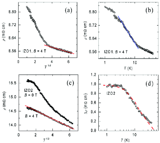
We start with our discussion on the IZO2 NW. Figure 6(c) shows the resistivity of the IZO2 NW as a function of in both = 0 and in a perpendicular = 4 T, as indicated. Clearly, the 4-T data illustrate a robust linear dependence between 3 and 40 K. Such a temperature dependence manifests the 3D EEI effect in this wide interval. By comparing with the prediction of equation (6), we obtained a value 0.42. This magnitude of is in line with that found in typical doped semiconductors, such as Si:B Dai92 . On the other hand, in = 0, the dependence of is somewhat more complicated, because both the WL and the EEI effects now contribute to the total resistivity rise. Using = 2.2 cm2/s (table 2), we estimate (5 K) 18 nm. This length scale is basically the conduction shell thickness inferred from the WL MR studies (section 3). That is, the 3D EEI effect on the resistivity rise is expected to persist from intermediately high down to 5 K in this particular NW. This prediction is in good accord with the observation depicted in figure 6(c).
Figure 6(d) plots the variation of the difference in the measured resistivity, = ( = 0) ( = 4 T), with temperature of the IZO2 NW whose resistivities are shown in figure 6(c). This figure indicates an approximate ln temperature dependence of between 3 and 40 K. This observation is meaningful. Indeed, this can be identified as originating from the 2D WL effect, which is theoretically predicted to be given by Altshuler85 , in terms of the normalized sheet resistance,
| (7) |
where is an arbitrary reference temperature, and and are defined below equation (2). Writing = and substituting the fitted values of and from our MR data analyses described in section 3 into equation (7), we obtain the dashed curve shown in figure 6(d), which is seen to satisfactorily describe the experimental . This result strongly confirms our scenario of the quantum-interference transport through a surface layer in single IZO NWs. Recall that the 2D WL MR effect in the IZO2 NW has been observed in the same interval of 1–40 K (subsection 3.2). Below about 3 K, tends to saturate to a constant value, because becomes very weakly dependent on , as shown in figure 4(b).
We turn to the IZO1 NW. For simplicity, we shall present and discuss only the data measured in a perpendicular = 4 T. Figure 6(a) shows that the law holds between 14 and 40 K. By comparing with equation (6), we obtained a value of 0.61. In contrast to the case of the IZO2 NW, a change in the dependence to the 2D ln law is seen between 3.6 and 11 K in this NW, see figure 6(b). By writing = and comparing with the prediction of equation (5), we obtained a value 0.51. This value is reasonably in line with that inferred above from the high- 3D regime. Thus, a dimensionality crossover with regard to the EEI effect does occur in the 11–14 K temperature window in this particular NW. In fact, using = 3.6 cm2/s (table 2), we estimate (11 K) = 16 nm. This value is very close to the conduction shell thickness 15 nm inferred from the WL MR studies discussed in section 3. In other words, at 11 K, and the EEI effect is 3D (figure 6(a)), while at 11 K, and the EEI effect is 2D (figure 6(b)). In short, the observations of a 2D-to-3D dimensionality crossover in both the EEI effect and the WL effect strongly substantiate the existence of an outer conduction shell of a thickness in IZO NWs.
Finally, it may be readily estimated that the thermal lengths = 52/ nm in the IZO1 NW and 41/ nm in the IZO2 NW. These lengths are relatively short, as compared with . Thus, a dimensionality crossover of the EEI effect from the 2D to the 1D regime is not seen in this experiment. Table 1 summarizes the various intervals over which different dimensionalities in the WL and the EEI effects are observed in this work.
V Electron dephasing time
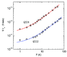
In this section, we analyze the dependence of to study the electron dephasing processes in IZO NWs. Recall that, for a given IZO NW, the “correct” values in different regions are those extracted according to the appropriate WL MR expressions in different dimensionalities. Figure 7 plots our extracted as a function of for the IZO1 and IZO2 NWs, as indicated. In this figure, the values of the IZO1 NW are a combination of those extracted according to the 1D WL form (equation (1)) between 1 and 8.5 K and those extracted according to the 2D WL form (equation (3)) between 7 and 50 K. The values of the IZO2 NW are a combination of those extracted according to the 2D WL form (equation (3)) between 1 and 40 K and those extracted according to the 3D WL form (equation (2)) between 40 and 70 K.
The physical meaning of is examined in the following. The total electron dephasing rate in a weakly disordered degenerate semiconductor can be written as Lin-jpcm02
| (8) |
where is a constant or a very weakly dependent quantity, whose origins (paramagnetic impurity scattering, dynamical structural defects, etc.) are a subject of elaborate investigations in the past three decades Birge03 ; Lin-prb87b ; Mohanty97 ; Huang-prl07 . The quasi-elastic (i.e., small-energy-transfer) Nyquist electron-electron (-) relaxation rate, , in low-dimensional disordered conductors is known to dominate in an appreciable interval. In the following analyses, we use the standard expression: = , where = 2/3 and 1 for 1D and 2D samples, respectively Altshuler85 ; Lin-jpcm02 ; Altshuler82 . Note that, as increases, the exponent of temperature in is expected to change as the sample dimensionality changes in our IZO NWs. The third term, , on the right-hand side of equation (8) denotes any additional inelastic scattering mechanism(s) that might play a role in the dephasing process at sufficiently high .
Before comparing our experimental data with equation (8), we first would like to comment on the electron-phonon (-ph) relaxation process. In disordered metals, the -ph scattering is often significant at a few degrees of kelvin and higher. One may then safely identify the term in equation (8) as the -ph scattering rate Sergeev-prb00 , in either the diffusive limit Lin-epl95 ; Zhong-prl98 or the quasi-ballistic limit Zhong-prl10 , depending on the experimental conditions. However, the carrier concentrations 1 cm-3 (table 2) in our IZO NWs, which are 3 to 4 orders of magnitude lower than those in typical metals Kittel . Theoretical evaluations show that at such carrier concentrations, the deformation potential still has a metallic nature, but substantially decreases due to the low concentration. The corresponding -ph coupling constant (the constant in Sergeev-prb00 ; Zhong-prl10 ) is found to be proportional to . Therefore, the -ph relaxation must be negligible in this work note9 . On the contrary, it should be pointed out that the - scattering in the IZO material relative to that in typical metals is enhanced, owing to the smaller value and the larger () value in IZO NWs.
In 3D, it is established that the - scattering is determined by the large-energy-transfer processes. In the clean limit, the theory Altshuler85 ; Lin-jpcm02 predicts = . Substituting the values of our IZO NWs into this expression, we estimate this scattering rate to be 4 s-1 ( 8 s-1) in the IZO1 (IZO2) NW. Even at a moderately high of 40 K, this scattering rate is more than (about) one order of magnitude smaller than the experimental value in the IZO1 (IZO2) NW. Therefore, this clean-limit - scattering process can be ruled out in the present study. In the dirty limit, the large-energy-transfer - scattering rate is modified to be = , with the coupling strength given by Altshuler85 ; Lin-jpcm02 ; Altshuler82
| (9) |
This scattering rate is relevant to our experiment at high values where our NWs enter the 3D WL regime.
Since the dimensionality crossover in the WL effect is less complex in the IZO2 NW, we first analyze the data in this sample. In this NW, there is a single 2D-to-3D crossover in the wide interval of 1–70 K. Therefore, we may rewrite equation (8) in the following form: = + + , where and denote the - scattering strength in the 2D and 3D regimes, respectively. (One may identify as the term in equation (8).) By least-squares fitting this expression to the experimental data (see figure 7), we obtain 9.0 K-1 s-1 and 2.2 K-3/2 s-1. Theoretically, the Nyquist - scattering strength in 2D is given by Altshuler85 ; Lin-jpcm02 ; Altshuler82
| (10) |
Substituting our experimental value of into equation (10), we obtain = 1.8 K-1 s-1. Also, substituting our experimental values of and into equation (9), we obtain = 2.7 K-3/2 s-1. These values are in good agreement with the experimental values. Therefore, we can clearly identify the - scattering as the dominating dephasing process in the IZO2 NW. We notice that our value is on the same order of magnitude as that found in the ZnO surface wells Goldenblum99 .
Our fitted value for the IZO2 NW is listed in table 3. It should be noted that the fitted value is only approximate, because we have not extensively measured the MR curves at subkelvin values to unambiguously extract = ( 0 K). We also note that, at our lowest measurement temperature of 1 K, the electrons in the NW might have been slightly overheated.
The electron dephasing processes in the IZO1 NW is somewhat more complicated and requires a more detailed examination. Because both 1D-to-2D and 2D-to-3D dimensionality crossovers in the WL effect are observed, we first write equation (8) in the form = + + to extract the values of and using data in the 10–50 K interval. Then, we write equation (8) in the form = + to extract the values of and using data in the 2–10 K interval. Our fitted result in figure 7 is obtained with the following values: 1.6 K-2/3 s-1, 1.1 K-1 s-1, and 2.3 K-3/2 s-1. Substituting our experimental value of into equation (10), we obtain = 2.4 K-1 s-1. Substituting our experimental values of and into equation (9), we obtain = 9.8 K-3/2 s-1. Our experimental values are within a factor of 2 of the 2D and 3D theoretical values, and thus are satisfactory.
In 1D, the Nyquist - scattering strength is theoretically predicted to be Hsu-prb10 ; Altshuler85 ; Altshuler82
| (11) |
Substituting our measured NW resistance , length , and diffusion constant into equation (11), we obtain 2.5 K-2/3 s-1. This value is about 50% higher than our experimental value, and hence our result is well acceptable note10 .
VI Conclusion
We have measured the temperature dependence of resistance as well as the magnetic field dependence of magnetoresistance in two indium-doped ZnO nanowires. The doped NWs reveal overall metallic transport properties characteristic of disordered conductors. Our results lead to our proposition of a core-shell-like structure in individual IZO NWs, with the outer shell of a thickness 15–17 nm being responsible for the observed quantum-interference WL and EEI effects. As a consequence, 1D-to-2D and 2D-to-3D dimensionality crossovers in the WL effect are evident as the temperature gradually increases from 1 to 70 K. A 2D-to-3D dimensionality crossover in the EEI effect has also been observed. A crossover to the 1D EEI effect is not seen, because the thermal diffusion length is relatively short, as compared with the effective NW diameter . These observations reveal the complex and rich nature of the charge transport processes in group-III metal doped ZnO NWs. In addition, we have explained the inelastic electron dephasing times. It should be emphasized that our experimental observation of a core-shell-like structure in IZO NWs is in good accord with the current theoretical understanding for impurity doping of semiconductor nanostructures. This result could have significant bearing on the potential implementation of nanoelectronic devices.
Acknowledgements.
This work was supported by the Taiwan National Science Council through Grant No NSC 100-2120-M-009-008 and by the MOE ATU Program (JJL). Research by JGL was supported by NSF.∗Email: jjlin@mail.nctu.edu.tw (Juhn-Jong Lin)
References
- (1) Nazarov Y V and Blanter Y M 2009 Quantum Transport: Introduction to Nanoscience (Cambridge: Cambridge University Press)
- (2) Chiquito A J, Lanfredi A J C, de Oliveira R F M, Pozzi L P and Leite E R 2007 Nano Lett. 7 1439
- (3) Lin Y H, Sun Y C, Jian W B, Chang H M, Huang Y S and Lin J J 2008 Nanotechnology 19 045711
- (4) Chiu S P, Chung H F, Lin Y H, Kai J J, Chen F R and Lin J J 2009 Nanotechnology 20 105203
- (5) Hsu Y W, Chiu S P, Lien A S and Lin J J 2010 Phys. Rev. B 82 195429
- (6) Yang P Y, Wang L Y, Hsu Y W and Lin J J 2012 Phys. Rev. B 85 085423
- (7) Tatara G, Kohno H and Shibata J 2008 Phys. Rep. 468 213
- (8) Rueß F J, Weber B, Goh K E J, Klochan O, Hamilton A R and Simmons M Y 2007 Phys. Rev. B 76 085403
- (9) Chiu S P, Lin Y H and Lin J J 2009 Nanotechnology 20 015203
- (10) Tsai L T, Chiu S P, Lu J G and Lin J J 2010 Nanotechnology 21 145202
- (11) Petersen G, Hernández S E, Calarco R, Demarina N and Schäpers Th 2009 Phys. Rev. B 80 125321
- (12) Liang D, Du J and Gao X P A 2010 Phys. Rev. B 81 153304
- (13) Hao X J, Tu T, Cao G, Zhou C, Li H O, Guo G C, Fung W Y, Ji Z, Guo G P and Lu W 2010 Nano Lett. 10 2956
- (14) Xu X, Irvine A C, Yang Y, Zhang X and Williams D A 2010 Phys. Rev. B 82 195309
- (15) Hernández S E, Akabori M, Sladek K, Volk Ch, Alagha S, Hardtdegen H, Pala M G, Demarina N, Grützmacher D and Schäpers Th 2010 Phys. Rev. B 82 235303
- (16) Zeng Y J, Pereira L M C, Menghini M, Temst K, Vantomme A, Locquet J-P and Van Haesendonck C 2012 Nano Lett. 12 666
- (17) Arutyunov K Yu, Golubev D S and Zaikin A D 2008 Phys. Rep. 464 1
- (18) Özgür Ü, Alivov Ya I, Liu C, Teke A, Reshchikov M A, Doğan S, Avrutin V, Cho S-J and Morkoc H 2005 J. Appl. Phys. 98 041301
- (19) Wang Z L 2008 ACS Nano 2 1987
- (20) Liu K W, Sakurai M and Aono M 2010 J. Appl. Phys. 108 043516
- (21) Ahn B D, Oh S H, Kim H J, Jung M H and Ko Y G 2007 Appl. Phys. Lett. 91 252109
- (22) Thompson R S, Li D, Witte C M and Lu J G 2009 Nano Lett. 9 3991
- (23) Look D C, Claflin B and Smith H E 2008 Appl. Phys. Lett. 92 122108
- (24) Bergmann G 1984 Phys. Rep. 107 1
- (25) Bergmann G 2010 Int. J. Mod. Phys. B 24 2015
- (26) Altshuler B L and Aronov A G 1985 Electron-Electron Interactions in Disordered Systems ed A L Efros and M Pollak (Amsterdam: Elsvier)
- (27) Schlenker E, Bakin A, Weimann T, Hinze P, Weber D H, Gölzhäuser A, Wehmann H-H and Waag A 2008 Nanotechnology 19 365707
- (28) Allen M W, Swartz C H, Myers T H, Veal T D, McConville C F and Durbin S M 2010 Phys. Rev. B 81 075211
- (29) Hu Y, Liu Y, Li W, Gao M, Liang X, Li Q and Peng L M 2009 Adv. Funct. Mater. 19 2380
- (30) Dalpian G M and Chelikowsky J R 2006 Phys. Rev. Lett. 96 226802
- (31) Ellmer K 2001 J. Phys. D: Appl. Phys. 34 3097
- (32) Hutson A R 1957 Phys. Rev. 108 222
- (33) Baer W S 1967 Phys. Rev. 154 785
- (34) Lien C C, Wu C Y, Li Z Q and Lin J J 2011 J. Appl. Phys. 110 063706
- (35) In the evaluation of in a given IZO NW, we have assumed that the electrical current passes through the whole volume of a NW. If the electrical conduction is not through the bulk of a NW, the above estimate of will be changed by an amount of 50%, according to the geometries of our core-shell-like structure. Since , the values of the other electronic parameters will thus be modified by smaller amounts of 15%. Such modifications will not affect any conclusions drawn in this work.
- (36) Lin J J and Bird J P 2002 J. Phys.: Condens. Matter 14 R501
- (37) Mani R G, von Klitzing K and Ploog K 1993 Phys. Rev. B 48 4571
- (38) Likovich E M, Russell K J, Petersen E W and Narayanamurti V 2009 Phys. Rev. B 80 245318
- (39) Andrearczyk T, Jaroszyński J, Grabecki G, Dietl T, Fukumura T and Kawasaki M 2005 Phys. Rev. B 72 121309(R)
- (40) Harmon N J, Putikka W O and Joynt R 2009 Phys. Rev. B 79 115204
- (41) Altshuler B L and Aronov A G 1981 JETP Lett. 33 499
- (42) Pierre F, Gougam A B, Anthore A, Pothier H, Esteve D and Birge N O 2003 Phys. Rev. B 68 085413
- (43) Shalish I, Temkin H and Narayanamurti V 2004 Phys. Rev. B 69 245401
- (44) Grinshpan Y, Nitzan M and Goldstein Y 1979 Phys. Rev. B 19 1098
- (45) Göpel W and Lampe U 1980 Phys. Rev. B 22 6447
- (46) Fukuyama H and Hoshino K 1981 J. Phys. Soc. Jpn. 50 2131
- (47) Wu C Y and Lin J J 1994 Phys. Rev. B 50 385
- (48) Reynolds D C, Litton C W and Collins T C 1965 Phys. Rev. 140 A1726
- (49) Baxter D V, Richter R, Trudeau M L, Cochrane R W and Strom-Olsen J O 1989 J. Phys. (Paris) 50 1673
- (50) Hikami S, Larkin A I and Nagaoka Y 1980 Prog. Theor. Phys. 63 707
- (51) Lin J J and Giordano N 1987 Phys. Rev. B 35 545
- (52) Equation (3) was originally formulated for a planar structure and with the field applied perpendicular to the film plane. In the present case, our conduction shell is roughly cylindrical. A similar situation occurred in multiwalled carbon nanotubes, where equation (3) had been successfully applied to describe the measured perpendicular MR in the 2D WL effect Langer-prl96, ; Tarkiainen-prb04, . In this work, by directly applying this equation also gave satisfactory fitting results of and for our IZO NWs. For example, we obtained 172 nm for both NWs. Moreover, the fitted values differed by less than 10–15% from those plotted in figures 4(a) and 4(b). In a strict manner, for a cylindrical film, the normal to the surface component of the field is not a constant but depends on the position of the surface component under consideration. In this case, the normal component of the applied field, , on each surface component has to be taken into account. In this work, we have approximated the cross section of the conduction shell in our NWs with a dodecagon and explicitly taken the field into our least-squares fits. A similar approach has recently been adopted in Blomers-nanolett11, for their analysis of InAs NWs, where the authors hypothesized a hexagonal cross section for their NWs.
- (53) Langer L, Bayot V, Grivei E, Issi J-P, Heremans J P, Olk C H, Stockman L, Van Haesendonck C and Bruynseraede Y 1996 Phys. Rev. Lett. 76 479
- (54) Tarkiainen R, Ahlskog M, Zyuzin A, Hakonen P and Paalanen M 2004 Phys. Rev. B 69 033402
- (55) Blömers Ch, Lepsa M I, Luysberg M, Gruẗzmacher D, Lüth H and Schäpers Th 2011 Nano Lett. 11 3550
- (56) Giordano N and Pennington M A 1993 Phys. Rev. B 47 9693
- (57) We note that a minute misalignment of the NW axis with respect to the field would cause an extra contribution from the perpendicular component of to the measured parallel MR data. In this experiment, we estimate that there could be a small misalignment of 5∘. Since the WL MR curves of the IZO NWs are not dramatically anisotropic, any possible tiny erroneous contribution from the perpendicular component of the field should thus be insignificant in this work.
- (58) Klamchuen A, Yanagida T, Kanai M, Nagashima K, Oka K, Seki S, Suzuki M, Hidaka Y, Kai S and Kawai T 2011 Appl. Phys. Lett. 98 053107
- (59) Altshuler B L, Aronov A G, Spivak B Z, Sharvin D Yu and Sharvin Yu V 1982 JETP Lett. 35 588
- (60) We notice that signatures of the AAS oscillations have recently been observed in radial core/shell In2O3/InOx heterostructure NWs Jung-nanolett08, . The authors found that the electrical current flowed dominantly through the core/shell interface, but not through the whole shell region. A very thin interface layer of sub-nanometer scale could sustain the AAS oscillations.
- (61) Jung M, Lee J S, Song W, Kim Y H, Lee S D, Kim N, Park J, Choi M-S, Katsumoto S, Lee H and Kim J 2008 Nano Lett. 8 3189
- (62) Aronov A G and Sharvin Yu V 1987 Rev. Mod. Phys. 59 755
- (63) Jian W B, Wu C Y, Chuang Y L and Lin J J 1996 Phys. Rev. B 54 4289
- (64) Lin J J and Wu C Y 1993 Phys. Rev. B 48 5021
- (65) Apart from equations (5) and (6), the EEI effect causes a temperature dependence of the resistance rise in 1D, which is not seen in this study.
- (66) Dai P, Zhang Y and Sarachik M P 1992 Phys. Rev. B 45 3984
- (67) Lin J J and Giordano N 1987 Phys. Rev. B 35 1071
- (68) Mohanty P, Jariwala E M Q and Webb R A 1997 Phys. Rev. Lett. 78 3366
- (69) Huang S M, Lee T C, Akimoto H, Kono K and Lin J J 2007 Phys. Rev. Lett. 99 046601
- (70) Altshuler B L, Aronov A G and Khmelnitsky D E 1982 J. Phys. C: Solid State Phys. 15 7367
- (71) Sergeev A and Mitin V 2000 Phys. Rev. B 61 6041
- (72) Lin J J and Wu C Y 1995 Europhys. Lett. 29 141
- (73) Zhong Y L and Lin J J 1998 Phys. Rev. Lett. 80 588
- (74) Zhong Y L, Sergeev A, Chen C D and Lin J J 2010 Phys. Rev. Lett. 104 206803
- (75) Kittel C 2005 Introduction to Solid State Physics (New York: Wiley)
- (76) Due to this relatively weak -ph coupling strength, one needs to be extremely careful about any possible electron overheating effect on the electrical-transport measurements at low . On the other hand, this relatively weak -ph coupling strength (partly) explains the reason why the quantum-interference WL MR can persist to 70 K in IZO NWs Wu-prb12, . We also would like to note that in a recent study of ZnO nanoplates with relatively low values, Likovich et al. Likovich09, have reported a law between 2 and 10 K. They also found a magnitude increased with increasing . More precisely, they reported (1.9 K) increased from 3.0 to 5.7 ns as increased from 1.3 to 7.4 cm-3. Although the authors had attributed their inelastic scattering rate to , these results seem to be hardly reconciled with the current understanding of the -ph relaxation process in degenerate semiconductors.
- (77) Goldenblum A, Bogatu V, Stoica T, Goldstein Y and Many A 1999 Phys. Rev. B 60 5832
- (78) Wu C Y, Lin B T, Zhang Y J, Li Z Q and Lin J J 2012 Phys. Rev. B 85 104204
- (79) We comment that, in the recent study of Ge/Si core/shell NWs by Hau et al. Hau10, , the authors had carried out two-probe MR measurements on a single NW over a very wide range of 0.4–150 K. They had applied the 1D WL MR form to this wide interval and in applied perpendicular fields up to as high as 8 T. Hau et al. then interpreted their extracted in terms of equation (11) alone. It is puzzling why the - scattering with large-energy transfer and other inelastic electron scattering processes did not play any role even up to such a high of 150 K. It is also not clear if any dimensionality crossover in the WL effect had taken place in the sample. These issues need further clarification.