JARA-FIT and 2nd Institute of Physics, Otto-Blumenthal-Straße, 52074 Aachen, Germany, EU
Quantum interference effects in resonant Raman spectroscopy of single- and triple-layer MoTe2 from first principles
Abstract
We present a combined experimental and theoretical study of resonant Raman spectroscopy in single- and triple-layer MoTe2. Raman intensities are computed entirely from first principles by calculating finite differences of the dielectric susceptibility. In our analysis, we investigate the role of quantum interference effects and the electron-phonon coupling. With this method, we explain the experimentally observed intensity inversion of the vibrational modes in triple-layer MoTe2 with increasing laser photon energy. Finally, we show that a quantitative comparison with experimental data requires the proper inclusion of excitonic effects.
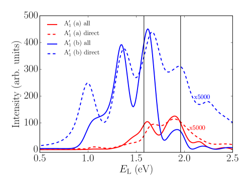
1 Introduction
Transition metal dichalcogenides (TMDs) are good candidates for nanoengineering due to their quasi-two-dimensional nature. The weak interlayer interaction allows the fine-tuning of the electronic and vibrational properties of the nanostructure by stacking different types and numbers of layers.1
To characterize the properties of these nanostructures, Raman spectroscopy is a useful and accurate technique, which simultaneously probes their vibrational and optical properties. It yields information about the lattice symmetry, the vibrational eigenmodes, and optically active electronic transitions, including excitonic effects.2, 3
In particular, when in the resonant regime, the Raman intensities show a strong dependence on the laser photon energy for certain phonon modes, as was shown for MoSe2,4, 5 MoS2,6 and WS2.7 This dependence allows the identification of excitonic states and the investigation of their coupling to phonons, as demonstrated for MoS2,8, 9 WS2, and WSe2.10 In MoTe2, measurements also show such a strong dependence.11, 12, 13, 14, 15 In the case of triple-layer MoTe2, it was observed that the intensity ratio between the lowest- and highest-frequency modes belonging to the same Davydov triplet significantly changes with laser photon energy.13, 14, 15 The change of the Raman intensities with laser photon energy in MoTe2 and in TMDs in general is yet to be fully understood and few ab initio studies are present in the literature.16 More recently, the experimental observation of the temperature dependence of the Raman intensities was reported.17 Single-layer MoTe2 is a near-infrared (1.1 eV at room temperature) direct optical band gap semiconductor, as such it is possible to probe excitonic states with visible photon energies.12, 18 Additionally the Davydov split modes appear prominently at visible (hence easily available) laser photon energies.13, 14, 15
In this work, we explain the dependence of the one-phonon Raman intensities on the laser photon energy using computational simulations and compare them with experimental results. The accurate description of resonant Raman scattering is challenging due to the interplay between electronic correlation and electron-phonon coupling. Up to now, most theoretical studies have focused on the non-resonant regime using simpler models like the bond-polarizability model or density functional perturbation theory.19, 20, 21 However, these methods assume static electromagnetic fields, which is not applicable in the resonant case where the dynamic dielectric response needs to be accounted for. Resonant Raman spectroscopy has also been studied using empirical models fitted from experiments to describe the electronic bands, phonon dispersion and electron-phonon coupling.22 More recently, a study on the double-resonant Raman process in MoTe2 investigated the resonance surface using calculations of the electronic structure and phonon dispersion.16
Here we use an ab initio approach to calculate the first-order Raman susceptibility as a function of laser photon energy. We calculate the Raman susceptibility by approximating the derivative of the dielectric response function with respect to lattice displacements with finite differences.23, 10 To this end, we combine different ab initio methods: we calculate the ground state properties using density functional theory (DFT), the phonons with density functional perturbation theory (DFPT), and the optical absorption spectra both in the independent-particle approximation and including many-body effects. We discuss the main qualitative features on the independent-particle level and show that the inclusion of excitonic effects provides a reliable quantitative description of the Raman spectrum, in very good agreement with experimental results. Moreover, the calculations reproduce the experimentally reported13, 14, 15 dependence of the intensity ratio of the Davydov triplet as a function of laser photon energy. Finally we give an explanation of the results in terms of quantum interference effects.
2 Raman intensities from first principles
The experimental observable of interest, the Raman intensity, is, in the case of phonon emission (Stokes scattering), given by3, 24, 2
| (1) |
Here, is the Raman susceptibility tensor, and are the polarization vectors of the incoming and scattered light, respectively, is the frequency of the incoming light, denotes the frequency of phonon mode , and represents its occupation factor. In the frozen-phonon limit, the Raman tensor equals the change of the dielectric susceptibility with atomic displacements2
| (2) |
where is the position of atom in the Cartesian direction , and the eigenvector of the phonon mode , normalized according to
| (3) |
where denotes the mass of atom . This formulation allows us to account for many-body effects in the Raman susceptibility by incorporating them in the calculation of the dielectric response. At this level, different well-tested implementations are available in a fully ab initio framework which allow the inclusion of excitonic and electronic correlation effects, which are especially relevant in TMDs.25, 26
The frozen-phonon approximation is valid at energies that fulfill the condition
| (4) |
where represents the energy of an electronic transition, is the photon energy of the incoming laser light (from now on designated simply as laser energy) and is the broadening, i.e., the inverse lifetime, of the electronic excitation. In the non-resonant regime, is far away from any electronic transition energy and this condition is automatically satisfied. In the resonant regime, where the laser energy always matches the energy of an electronic transition, the relevant condition is that the phonon energy (20-25 meV) is smaller than the electronic broadening. At room temperature the broadening due to electron-phonon coupling is around 100 meV27 and therefore the frozen-phonon approximation is reasonable.
This approach explicitly captures the laser-energy dependence inherent to the Raman susceptibility tensor, which is crucial for studying resonance effects. This formulation goes beyond the bond polarizability model and DFPT, which assume static electromagnetic fields, and are therefore only valid in the non-resonant regime.28, 29
2.1 Electronic structure and phonons
The electronic structure of MoTe2 is calculated using DFT within the local density approximation (LDA), as implemented in the PWscf code of the Quantum ESPRESSO suite.30 We include the semi-core 4s and 4p states in the pseudopotential of molybdenum and account for spin-orbit interaction by employing spinorial wave functions. The charge density is calculated using a plane-wave energy cutoff of 100 Ry and a -point grid for both the single- and triple-layer calculation. For the lattice parameter, we use the experimental value of 3.52 Å. 31
| Mode | |||
|---|---|---|---|
| Raman tensor | |||
| Single-layer | 174.6 (171.5) | 238.3 (236.5) | |
| Freq. (cm-1) | |||
| Triple-layer | (a) 173.6 (169.4) | 235.5 (234.7) | |
| Freq. (cm-1) | 175.1 | 238.0 | |
| (b) 176.4 (172.6) | 239.0 (234.7) | ||
The phonons of MoTe2 are calculated using DFPT. Due to momentum conservation, only phonon modes at participate in first-order Raman scattering, as the magnitude of the light momentum is negligible compared to the crystal momentum. The Raman-active phonon modes of interest are reported in Table 1. Both single- and triple-layer MoTe2 belong to the space group D3h. We refer to the different phonon modes by their irreducible representation label in the Mulliken notation. The phonon modes of single-layer MoTe2 are denoted by and for the in-plane and out-of-plane modes, respectively.32 When going from single-layer to triple-layer MoTe2, the mode splits into a Davydov triplet composed of two Raman-active modes, which we denote by (a) and (b), and one IR-active mode. In this work, we will study the experimentally observed inversion of the Raman intensity ratio between the (a) and (b) modes as a function of laser energy as shown in Figure 1.
2.2 Optical absorption
We calculate the optical absorption on two levels of theory: in the first approach, we treat electrons and holes as independent particles (IP), while in the second case, we include many-body effects due to electron-electron and electron-hole interaction perturbatively using the GW approximation and Bethe-Salpeter equation (BSE).33
2.2.1 Independent-particle approximation
The expression for the IP dielectric susceptibility can be derived from time-dependent perturbation theory and is given by 34
| (5) |
where denotes the electron-light coupling (ELC) matrix elements, also referred to as dipole matrix element, and and are the DFT valence and conduction bands energies, respectively. The index denotes the Cartesian component of the ELC, while the parameter represents the sum of the electron and hole broadening. We use a constant broadening of 100 meV. The calculation of the ELC was performed using the yambo code. 35 The absorption spectrum is proportional to the imaginary part of the diagonal elements of the dielectric susceptibility tensor .
2.2.2 Many-body perturbation theory
The two-dimensional character of MoTe2 reduces the dielectric screening and hence many-body effects are more pronounced than in three-dimensional materials. Such effects manifest themselves as significant corrections to the electronic band energies and in large excitonic binding energies. We account for these effects by combining the GW method and the BSE.36 GW calculations were performed non-self-consistently (G0W0) using a sampling of the Brillouin zone (BZ) and a 40 Ry cutoff for the plane-wave basis. A converged quasi-particle band gap was obtained by including 120 electronic bands for single- and 360 bands for triple-layer MoTe2. It should be noted that an accurate GW correction requires the inclusion of the semi-core states in the Mo pseudopotential.37 In order to avoid spurious interactions between periodic copies of the layers along the z-direction, we apply a Coulomb cutoff.38
We account for electron-hole interactions by solving the BSE with a statically screened Coulomb potential.36 In terms of exciton energies , exciton-light coupling matrix elements , and excitonic broadening , the dielectric susceptibility reads:
| (6) |
The BSE calculations were performed using a 30 Ry cutoff for the plane-wave basis and a -point grid to sample the Brillouin zone. We include electronic transitions inside a 3 eV window (see Supporting Information for details of the GW and BSE calculations).
2.3 Raman susceptibility tensor
The Raman susceptibility tensor of phonon mode is calculated by approximating the directional derivative of with the finite differences method. For this, we evaluate the dielectric susceptibility at the two displaced positions and divide by the amplitude of the two displacements.
An important practical drawback of this method is that the displacements according to certain phonon modes break some symmetries of the crystal. This in turn increases the computational cost of the calculation with respect to the fully symmetric absorption calculation. To reduce the computational cost, we extrapolate the GW correction from the undisplaced to the displaced case using a scissor operator, which incorporates the stretching of the bands. This scissor operator is kept fixed for all calculations (see Supporting Information). In addition, note that both the real and imaginary part of the dielectric susceptibility enter in the calculation of the Raman susceptibility. The real part is known to converge more slowly with the number of bands.
In the IP picture we can further analyze the Raman susceptibility tensor by splitting it up into the contributions from individual -points. To this end, we note from Eq. 5 that we can represent the susceptibility as a sum over :
| (7) |
where the term contains contributions from all electronic transitions at that -point. Analogously, we write the Raman susceptibility from Eq. 2 as .
Contrary to the dielectric susceptibility, in which is the sum of all , the Raman intensity is the square of the sum of :
| (8) | ||||
The interference terms can be constructive or destructive. If enough electronic transitions with a finite amplitude are in phase we detect a large Raman intensity. However, if the contributions are out of phase, interference will lead to a small or even zero Raman intensity. The weight of the direct terms in the final result is much smaller than that of the interference terms (see Supporting Information).
The key point of this paper is to use the concept of quantum interference to explain the observed behavior of the Raman intensity with laser energy in MoTe2. This concept was shown to be important in the Raman intensities of graphene where an increase of the Raman intensity is observed when destructive interference terms are Pauli-blocked through electron or hole doping.39, 40, 41, 42 We show that selection rules manifest themselves at the level of quantum interference, but even when selection rules do not apply, quantum interference explains the behavior of the Raman intensity. Since interference effects reflect the interplay of all the terms , it is inaccurate to attribute the features in the behavior of the Raman intensities to a single electronic transition.
3 Results
3.1 Experimental results
Single- and few-layer hexagonal MoTe2 (hereafter simply denoted MoTe2) samples were prepared by mechanical exfoliation and deposited onto Si substrates covered with a 90 nm SiO2 epilayer. The Raman spectra of single- and triple-layer MoTe2 were measured at three different laser energies (, 1.96 eV, and 2.33 eV) in a backscattering geometry using a custom-built micro-Raman setup. The incoming laser beam was linearly polarized and the Raman scattered light was sent through a monochromator with a 500 mm focal length coupled to a charge-coupled device (CCD) array. A 900 (resp. 2400) lines/mm grating was used for measurements at 1.58 eV (resp. 1.96 eV and 2.33 eV). Laser intensities below were employed in order to avoid photoinduced heating and sample deterioration. The Raman spectra were fit with Voigt profiles taking into account the spectral resolution of our setup of 1.0, 0.4 and 0.6 cm-1 at 1.58 eV, 1.96 eV, and 2.33 eV, respectively. Figure 1 shows micro-Raman spectra of single- and triple-layer MoTe2. The number of MoTe2 layers has been unambiguously identified as described in Ref.13. The raw spectra have been normalized by the integrated intensity of the T2g (point group Oh) Raman mode of silicon at for a qualitative comparison. To quantitatively compare experimentally measured Raman intensities with the ab initio Raman susceptibilities calculated according to Eq. 1, we have also taken optical interference effects into account and extracted the -component of the Raman susceptibility after carefully considering the polarization-dependent response of our setup. Additional details on the normalization procedure can be found in the Supporting Information.
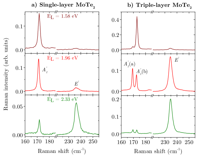
In Figure. 1, we show the experimentally obtained Raman spectra of single- (panel (a)) and triple-layer (panel (b)) MoTe2. The prominent A and E′ modes are clearly visible. In single-layer MoTe2, the A mode dominates the spectrum at laser energies of =1.58 and 1.96 eV, while at =2.33 eV the E′ mode is dominant. Similarly, in triple-layer MoTe2, the and mode dominate the Raman spectra at and , respectively. However, the modes feature and the mode have comparable intensities at .
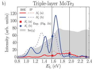
Remarkably, the Davydov-split (a) and (b) modes have similar intensities in triple-layer MoTe2 at and , whereas the bulk-like (b) mode is 13 times more intense than the (a) mode at . Note that the mode does not display a measurable Davydov spitting.13 In Figure 2, we will compare the experimentally measured Raman susceptibilities and integrated intensity ratios between the (b) and (a) modes with ab initio calculations and correlate the observation of a prominent Davydov splitting with resonantly enhanced Raman intensities.
3.2 Theoretical calculations
In the following we will discuss the results of first-principles calculations and compare them with our experimental results. Before discussing the results for triple-layer MoTe2, we analyze the single-layer case. This allows us to introduce the concept of quantum interference in a simpler context. In all cases we will analyze the -component of the Raman susceptibility tensor, . The other components are related to -component of , as shown in Table 1.
3.2.1 Single-layer MoTe2
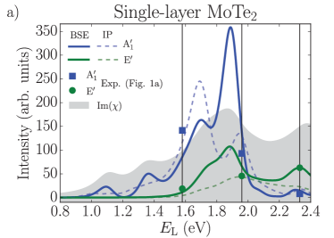
In the case of single-layer MoTe2, we analyze the Raman susceptibility for the and modes. Figure 2a shows the Raman susceptibility as a function of laser energy for both the IP (dashed lines) and BSE calculations (solid lines). Up to a laser energy of 2 eV the intensity of the mode is larger than that of the mode. At higher laser energy, the mode has a larger intensity than the mode, in good agreement with the experimental data reported here and in the literature.12, 13, 14 The overall scale of the theoretical results (IP- and BSE-level) is has been chosen to reflect that of the experimental results. This chosen scale is the same for both the IP- and BSE-level calculation to allow a comparison between the two. Since the overall scaling factor cancels when considering intensity ratios, the quantity that can be compared unambiguously between experiment and theory is the ratio of two intensities, as shown in Figure 2c and d. The inclusion of many-body effects does not change this general trend but affects the relative intensities at the excitonic transitions.


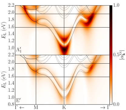
We first analyze the contributions of the individual -points to the IP susceptibility . Figure S2a shows along a path through the high-symmetry points in the BZ. The main contributions to for laser energies between 0.8 and 2 eV come from the lower bands in transition space in a region around K and between K and M.
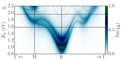
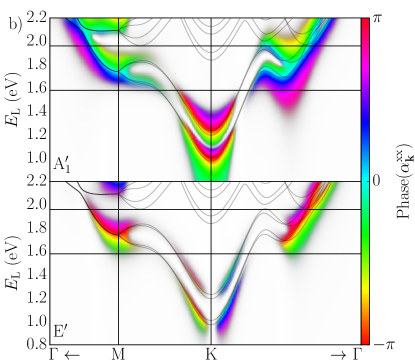
It should be noted that only optically active transitions can contribute to the Raman susceptibility, but not all of them necessarily do so. For instance, near the band gap, the mode is active while the mode is silent, even though the same electronic transitions contribute and both modes are, in principle, allowed by lattice symmetry. This behavior can be understood in terms of angular momentum conservation. Near the band gap at K the band structure is rotationally symmetric and thus angular momentum is conserved. Both incoming and outgoing photons carry an angular momentum of while the phonon does as well. This implies that the final state has a total angular momentum of or , which violates angular momentum conservation and renders the mode silent. By contrast, the phonon corresponding to the mode does not carry angular momentum and hence the corresponding process is allowed.
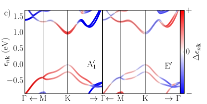
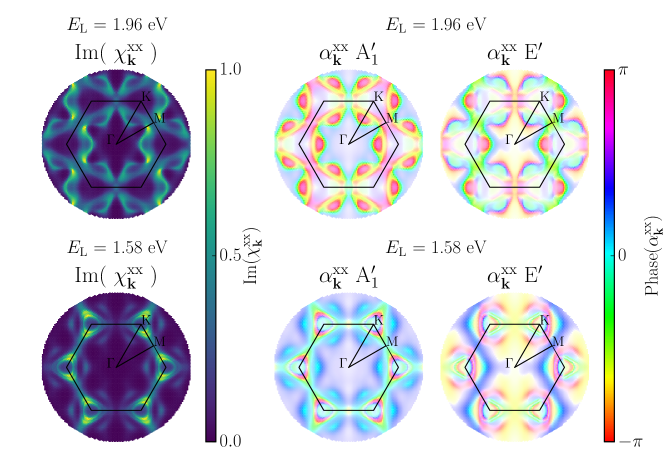
This can also be understood from the point of view of quantum interference. For this purpose, we show the -resolved Raman susceptibly as a function of in Figure S2b. We color-encode the phase when the amplitude is larger than 7% of the maximum amplitude at that laser energy. For the mode, the positive contribution from one side of the valley is added to the negative contribution from the other side, which leads to an overall cancelation of the Raman intensity. By contrast, for the mode the contributions add up constructively. At higher laser energies, the full rotation symmetry gradually gets broken down to the 120∘ rotation symmetry of the lattice, an effect known as trigonal warping43 of the electronic structure. Angular momentum is then only conserved up to integer multiples of and both the and modes become allowed.
In order to track down the origin of the phase of the Raman susceptibility, we take a closer look at the derivative of () with respect to atomic displacements:2
| (9) |
where .
The first term involves the change of the electronic band energies, which is given by the diagonal (intra-band) electron-phonon coupling (EPC) matrix elements. The second term stems from the change of the ELC upon atomic displacements and involves the off-diagonal EPC matrix elements. The first term is double-resonant and corresponds to a process where an electron is excited to a conduction band, then scatters with a phonon within the same band, and finally decays to the valence band by emitting a photon. Since this term is double-resonant, we assume it to be dominant and we can directly relate the phase of the Raman susceptibility with the sign of the diagonal EPC matrix elements. We visualize these by plotting the change of the electronic band energies with respect to atomic displacements, which correspond to the diagonal EPC matrix elements, as shown in Figure S2c. From this plot we observe a direct correlation between the sign of the diagonal EPC and the phase of the Raman susceptibility in Figure S2b. Therefore, we attribute constructive or destructive interference between regions of the BZ to differences in sign of the change of the electronic band energies.
3.2.2 Triple-layer MoTe2
In the case of triple-layer MoTe2, we focus our attention on the (a) and (b) modes, for which experiments reported here and in the literature13, 14, 15 show a variation of the relative Raman intensity as a function of laser energy. Our calculations, both on the IP and BSE level, reproduce this observation very well, as shown in Figure 2b and d. Common to both calculations is that the (a) phonon mode is dominant in intensity for laser energies up to 1.8 eV while at higher laser energies the (b) mode is dominant. However, only with the inclusion of excitonic effects (BSE) do we obtain the experimentally observed ratio. Contrary to the single-layer case, where the different intensities are related to different symmetries of the phonon modes, in the triple-layer case, the (a) and (b) modes belong to the same representation and hence symmetry based-arguments do not apply. However, we can still use the concept of quantum interference introduced previously to explain the intensity inversion.
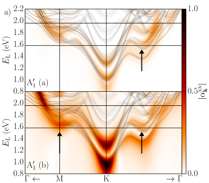
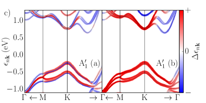
We start by analyzing the behavior of the Raman susceptibility for laser energies near the band gap energy. There, the (b) mode has a large intensity while the (a) mode is practically silent. This can be understood from Figure 4c, where we show the diagonal EPC matrix elements along the high-symmetry line in the BZ. For the (b) mode the conduction band states at K contribute with the same sign, while for the (a) mode they have opposite signs. This is a direct consequence of the band composition at K and the way the layers vibrate (in-phase in the (b) mode and out-of-phase in the (a) mode, respectively - see Supporting Information) .
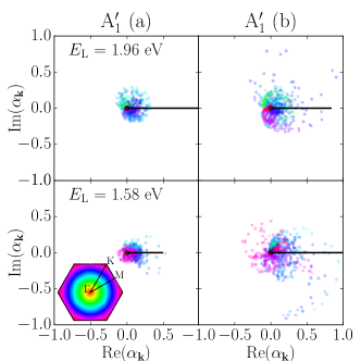
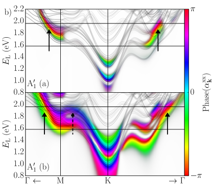
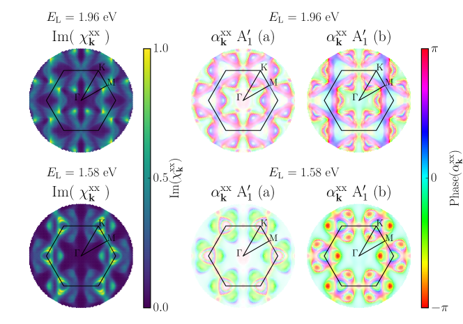
The Raman intensities at higher laser energies (between 1.58 and 1.96 eV) can also be understood from the point of view of quantum interference. For this, we represent the contributions from all -points in the BZ as points in the complex plane (“Argand plot”) as shown in Figure 5. By color-encoding the -point location in the BZ, we can identify the regions which contribute constructively to the total Raman amplitude and those that are interfering destructively. The overall phase of the different contributions has been fixed such that the total Raman susceptibility is real and positive (solid black line). At a laser energy of 1.58 eV, the contributions from the edge of the BZ, i.e., between K and M (purple dots), scatter concentrically around the origin and mostly cancel each other for both phonon modes. However, the regions between K and and M and (blue dots) are building the signal up. Since these contributions have larger amplitude for the (b) mode than for the (a) mode, the former has to a larger intensity at this laser energy. This becomes clear by looking at Figure 4, where we represent the absolute value of along the high-symmetry line in panel (a) and its phase in panel (b). For a laser energy of 1.58 eV, there are resonant transitions between K and and at M (see arrows in panel (a)). At these points the modulus of is large and the phases are the same, which leads to constructive interference of the signal and an increase in the observed Raman intensity for both phonon modes.
At a laser energy of 1.96 eV, the situation is rather different. The contributions from the region between K and M (purple dots in the Argand plot) no longer scatter concentrically around the origin and now destructively interfere with the contributions from the K- and M- regions (blue dots). We resolve which electronic transitions lead to these destructive interference effects by referring once more to Figure 4. The destructive contributions stem from transitions at M, which have a relative phase of (blue areas in Figure 4b) while the constructive ones have relative phases between and (green, yellow, and red areas).
In the case of the (a) mode, the amplitude of these destructive contributions is small and hence the resulting signal is larger than the one of the (b) mode, for which the destructive contributions have a sizable amplitude. From Figure 4a we can verify that both the amplitude of the near the M point is larger for the (b) mode and that their phases are opposite to the ones from the contributions of the constructively interfering points (see dashed and solid arrows in panel (b)).
The reason for the small amplitudes in the K-M region for the (a) mode can be deduced from Figure 4c. The diagonal EPC matrix elements for the (a) mode and the lowest conduction bands along the K-M direction have both positive and negative signs. Consequently, their contribution to () mostly cancels out, which leads to a small contribution to the Raman susceptibility. On the other hand, for the (b) mode, the different EPC matrix elements add up with the same sign and the -points from this region give a larger contribution.
4 Conclusions and Outlook
We calculated the laser energy-dependent Raman susceptibility in an ab initio framework by taking finite differences of the dynamic dielectric susceptibility in the frozen-phonon approximation. We applied our method to study the Raman spectrum of single- and triple-layer MoTe2, reproducing and explaining the experimentally observed behavior of the intensity ratio as a function of laser energy for the different phonon modes. We demonstrated that quantum interference effects between contributions of electronic transitions from different parts of the Brillouin zone are responsible for this behavior. We also found a correlation between the phase of these contributions and the sign of the diagonal electron-phonon coupling matrix elements. Quantum interference effects make the direct correlation of the optical absorption spectrum with the measured and calculated Raman intensities highly non-trivial. Additionally, we showed that symmetry arguments are not always enough to explain the counterintuitive behavior of the intensities as a function of laser photon energy as seen in the case of the modes of triple-layer MoTe2. Instead, a careful and detailed analysis is required to trace down which features of the electronic structure, vibrational spectra, and interplay between them are responsible for the observed behavior. Furthermore, we showed that the proper inclusion of excitonic effects is necessary to accurately describe the experimentally observed intensity ratio of the modes as a function of laser energy. The approach presented here offers a way to systematically analyze resonant Raman spectra. Because of its ab initio nature, it can be directly used to study different phonon modes of various materials in different phases. Additionally, it can also be applied to study the temperature dependence of the Raman spectrum, as recently investigated experimentally.17 This could be done by including the electron lifetimes and renormalization from electron-phonon coupling as recently shown for the temperature dependent optical absorption of MoS2.27
We thank Etienne Lorchat for fruitful discussions. The authors acknowledge support by the National Research Fund, Luxembourg (Projects OTPMD, RAMGRASEA, C14/MS/773152/FAST-2DMAT, and INTER/ANR/13/20/NANOTMD) and the Agence Nationale de la Recherche, France (under grant H2DH ANR-15-CE24-0016). S.B. is a member of the Institut Universitaire de France (IUF). The simulations were done using the HPC facilities of the University of Luxembourg 44. The authors declare no competing financial interests.
Supporting Information
S1 Ground state properties and phonons
Calculations of the electronic ground-state properties were done within density functional theory (DFT) in the local density approximation (LDA). Since LDA is known to underestimate the lattice parameters, we use the experimentally determined lattice constant of MoTe2, =3.52 Å31. We chose an LDA exchange-correlation function over more elaborate van der Waals functionals, as it has been shown to perform well in predicting vibrational properties of layered materials.20, 19
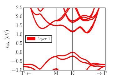
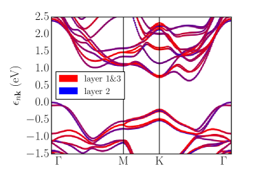
Figure S1 shows the electronic band structure of single- (left panel) and triple-layer (right panel) MoTe2. When passing from the single- to the triple layer case, each single-layer band splits into a triplet of bands. We represent the contributions of the different layers to the orbital composition of each band by color (red for the outer layers 1 and 3 and blue for the inner layer 2). This decomposition should be compared to Figure 4c in the main text, where the sign of the band energy change with atomic displacements according to the A(a) and (b) phonon modes is shown. In the case of the A(b) mode, the three layers vibrate in phase (see inset in Figure 1b of the main text) and hence the band energies within each band triplet always change with the same sign, independent of the layer composition of the bands. For the A(a) mode, on the other hand, the oscillation phase of the inner layer is opposite to that of the two outer layers (see inset in Figure 1b of the main text) and due to the different layer contributions to each band triplet member, the sign of the band energy changes varies within the triplet.
S2 Optical absorption
We calculated the GW quasi-particle correction to the LDA eigenvalues using the yambo code.35 We used a sampling of the Brillouin zone (BZ) for single- and triple-layer MoTe2. We used a 40 Ry cutoff for the plane-wave basis set, a Coulomb cutoff technique38 to avoid spurious interactions between the periodic copies in the z-direction and a vacuum separation of 50 and 70 Bohr for single- and triple-layer, respectively.
We calculated the GW quasiparticle corrections for the band gap and applied a scissor shift45 to the LDA band energies of the other bands to account for this corrections without having to compute them explicitly. The scissor operator is kept fixed for the different atomic displacements. This approximation has the advantage that only one calculation of the correction of the band gap energy is needed. However, it does not account for the changes of the screening effects in the electron-phonon interaction. A consistent way of including these corrections is still desirable and will be the topic of future work.
| scissor shift (eV) | |
|---|---|
| Single-layer | 0.667 |
| Triple-layer | 0.548 |
The calculation of the dielectric susceptibility including many-body effects has been performed by solving the Bethe-Salpeter equation (BSE) with the yambo code.35 The static dielectric screening was calculated using the same vacuum separation between the layers as in the GW case. The number of electronic transitions included to construct the BSE Hamiltonian was selected to include electronic transitions inside a energy window of 3 eV. We find this criterion to be more meaningful physically and the convergence of the spectra to be more stable compared to selecting the number of valence and conduction bands separately. Especially in the triple-layer case, we find many dispersive and crossing bands near the lower conduction and topmost valence band (see Figure S1b), which makes it difficult to know a priori how many bands need to be included in the calculation. Additionally, checking the convergence with the gradual inclusion of valence and conduction bands can lead to a false convergence of the dielectric susceptibility.
S3 Results
S3.1 Single-layer
As complementary information to the main text, we represent the intensity of the individual contributions in transition space for the two phonon modes (A and E′) of single-layer MoTe2 in Figure S2.
It is also instructive to look at the individual contributions over the full Brillouin zone (FBZ) as shown in Figure S3. A line cut along the high-symmetry points of this is shown in Figure 3 of the main text. However, there are additional contributions from regions not along the high-symmetry, shown in Figure S3. In all cases, we consider the contributions for incoming and outgoing light polarized along the x-direction. This leads to a breaking of some symmetries of the lattice and to the emergence of two inequivalent M and K points. We choose to represent the contributions along the high-symmetry line represented in Figure S3 to simplify the analysis without compromising the main conclusions. In the case of the mode the phonon was chosen to be polarized along the x-direction.
S3.2 Triple-layer
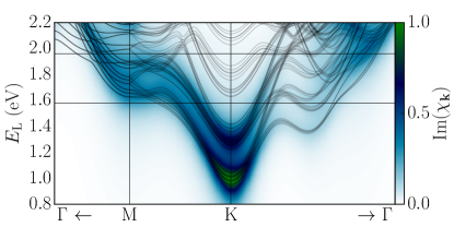
For the triple-layer case, we represent Im along the high-symmetry line in Figure S4. We additionally represent the individual contributions on the full BZ as represented in Figure S5 for the two energies (1.57 eV and 1.96 eV) used in our experiments. A line cut through this figure along the high-symmetry points is shown in Figure 4a of the main text. Similarly to the mode in single-layer, the symmetry is broken along the x-direction.
S4 Direct and interference terms
We performed calculations with and without the interference terms in the IP level. The omission of the interference terms leads to Raman intensities that are orders of magnitude smaller than those obtained by including them. This is consistent with the fact that the calculation of the interference terms involves two integrations over the Brillouin zone compared to only one integration for the “direct” terms (see Equation 8 in the main text). Thus their weight compared to the “direct” terms is in general much larger. Ignoring the interference terms leads to the absence of the observed intensity inversion of the Davydov multiplet of the A modes.
S5 Normalization procedure for the experimental data
To quantitatively compare Raman susceptibilities recorded at different laser photon energies, one has to carefully normalize the Raman spectra. Indeed, the spectra may not be acquired under the exact same conditions (e.g., different integration time, laser intensity,…) and the detection efficiency of the experimental setup may also be different. To get rid of all these dependencies, one can normalize the measured Raman intensities to the integrated intensity of a close-lying and well-known Raman feature. We chose the Raman mode of the bulk silicon substrate at around , which has been very well documented, for instance in Ref.46. Furthermore, one also has to take into account the dependence of the measured Raman intensity on the laser photon energy as well as optical interference effects.
Consequently, the normalized Raman intensity of a given Raman mode X is given by
| (S1) |
where is the incoming laser photon energy, is a coefficient that takes into account the resonance effect in the Si mode intensity as shown in Ref.46, and are the integrated intensity of the X and Si mode, and are the energies of the Raman scattered photons contributing to the X and Si modes, and and are the enhancement factors for the X and Si modes in the [Si/SiO2/single- or triple-layer MoTe2/air] layered system, respectively. Note that after applying Eq. (S1), the integrated intensity ratio only depends on . Let us also note that the term stems from the photon energy dependence of the Raman scattered energy flux () and from the fact that our detector -a charge-coupled device (CCD) array- measures a signal proportional the number of incoming photons, not to the energy flux. In the range of energies studied here, the coefficient is directly deduced from Figure 6 in Ref.46. The enhancement factors are obtained following Yoon et al.47 and Soubelet et al.4. To obtain reliable enhancement factors, we have first carefully estimated the refractive index of few-layer MoTe2 from the measurement of the intensity of the Si Raman mode in a [Si/SiO2/-layer MoTe2/air] layered system as a function of the number of layers , similarly to Zhang et al.48. Second, to accurately estimate the measured Raman signal from the Si substrate, we have considered the semi-transparency of bulk Si and the fact that we use a confocal Raman setup. Indeed, since bulk Si absorbs strongly in the visible range, the Si thickness that contributes to the Raman signal is much smaller than the Rayleigh length of our focused laser beam and the assumption of a semi-infinite Si layer is valid. However, bulk Si becomes quasi-transparent in the near-infrared region and a Si thickness on the order of the Rayleigh length contributes to the Raman signal. Therefore assuming that the Raman signal stems from a semi-infinite Si layer would lead to strong overestimation of the Si Raman signal4. Finally, in order to obtain a quantity proportional to the square modulus of the Raman susceptibility (see comparison between experimental and theoretical values in Figure 2 in the main text), we have also considered the distinct frequencies and occupation numbers of the and phonon modes (see Eq.1 in the main text).
References
- Geim and Grigorieva 2013 Geim, A. K.; Grigorieva, I. V. Nature 2013, 499, 419–425
- Cardona and Güntherodt 1982 Cardona, M.; Güntherodt, G. Light scattering in solids II: basic concepts and instrumentation; Springer-Verlag, 1982
- Loudon 1963 Loudon, R. Proceedings of the Royal Society of London A: Mathematical, Physical and Engineering Sciences 1963, 275, 218–232
- Soubelet et al. 2016 Soubelet, P.; Bruchhausen, A. E.; Fainstein, A.; Nogajewski, K.; Faugeras, C. Physical Review B 2016, 93, 155407
- Kim et al. 2016 Kim, K.; Lee, J.-U.; Nam, D.; Cheong, H. ACS Nano 2016, 10, 8113–8120
- Lee et al. 2015 Lee, J.-U.; Park, J.; Son, Y.-W.; Cheong, H. Nanoscale 2015, 7, 3229–3236
- Staiger et al. 2015 Staiger, M.; Gillen, R.; Scheuschner, N.; Ochedowski, O.; Kampmann, F.; Schleberger, M.; Thomsen, C.; Maultzsch, J. Physical Review B 2015, 91, 195419
- Carvalho et al. 2015 Carvalho, B. R.; Malard, L. M.; Alves, J. M.; Fantini, C.; Pimenta, M. A. Physical Review Letters 2015, 114, 136403
- Scheuschner et al. 2015 Scheuschner, N.; Gillen, R.; Staiger, M.; Maultzsch, J. Physical Review B 2015, 91, 235409
- del Corro et al. 2016 del Corro, E.; Botello-Méndez, A.; Gillet, Y.; Elias, A. L.; Terrones, H.; Feng, S.; Fantini, C.; Rhodes, D.; Pradhan, N.; Balicas, L. et al. Nano Letters 2016, 16, 2363–2368
- Yamamoto et al. 2014 Yamamoto, M.; Wang, S. T.; Ni, M.; Lin, Y.-F.; Li, S.-L.; Aikawa, S.; Jian, W.-B.; Ueno, K.; Wakabayashi, K.; Tsukagoshi, K. ACS Nano 2014, 8, 3895–3903
- Ruppert et al. 2014 Ruppert, C.; Aslan, O. B.; Heinz, T. F. Nano Letters 2014, 14, 6231–6236
- Froehlicher et al. 2015 Froehlicher, G.; Lorchat, E.; Fernique, F.; Joshi, C.; Molina-Sánchez, A.; Wirtz, L.; Berciaud, S. Nano Letters 2015, 15, 6481–6489
- Grzeszczyk et al. 2016 Grzeszczyk, M.; Gołasa, K.; Zinkiewicz, M.; Nogajewski, K.; Molas, M. R.; Potemski, M.; Wysmołek, A.; Babiński, A. 2D Materials 2016, 3, 025010
- Song et al. 2016 Song, Q. J.; Tan, Q. H.; Zhang, X.; Wu, J. B.; Sheng, B. W.; Wan, Y.; Wang, X. Q.; Dai, L.; Tan, P. H. Physical Review B 2016, 93, 115409
- Guo et al. 2015 Guo, H.; Yang, T.; Yamamoto, M.; Zhou, L.; Ishikawa, R.; Ueno, K.; Tsukagoshi, K.; Zhang, Z.; Dresselhaus, M. S.; Saito, R. Physical Review B 2015, 91, 205415
- Gołasa et al. 2017 Gołasa, K.; Grzeszczyk, M.; Molas, M. R.; Zinkiewicz, M.; Bala, L.; Nogajewski, K.; Potemski, M.; Wysmołek, A.; Babiński, A. Nanophotonics 2017, 0
- Froehlicher et al. 2016 Froehlicher, G.; Lorchat, E.; Berciaud, S. Physical Review B 2016, 94, 085429
- Luo et al. 2013 Luo, X.; Zhao, Y.; Zhang, J.; Xiong, Q.; Quek, S. Y. Physical Review B 2013, 88, 075320
- Luo et al. 2013 Luo, X.; Zhao, Y.; Zhang, J.; Toh, M.; Kloc, C.; Xiong, Q.; Quek, S. Y. Physical Review B 2013, 88, 195313
- Umari et al. 2001 Umari, P.; Pasquarello, A.; Dal Corso, A. Physical Review B 2001, 63, 094305
- Cantarero et al. 1989 Cantarero, A.; Trallero-Giner, C.; Cardona, M. Physical Review B 1989, 39, 8388–8397
- Gillet et al. 2013 Gillet, Y.; Giantomassi, M.; Gonze, X. Physical Review B 2013, 88, 094305
- Birman and Ganguly 1966 Birman, J. L.; Ganguly, A. K. Physical Review Letters 1966, 17, 647–649
- Qiu et al. 2013 Qiu, D. Y.; da Jornada, F. H.; Louie, S. G. Physical Review Letters 2013, 111, 216805
- Molina-Sánchez et al. 2013 Molina-Sánchez, A.; Sangalli, D.; Hummer, K.; Marini, A.; Wirtz, L. Physical Review B 2013, 88, 045412
- Molina-Sánchez et al. 2016 Molina-Sánchez, A.; Palummo, M.; Marini, A.; Wirtz, L. Physical Review B 2016, 93, 155435
- Lazzeri and Mauri 2003 Lazzeri, M.; Mauri, F. Physical Review Letters 2003, 90, 036401
- Veithen et al. 2005 Veithen, M.; Gonze, X.; Ghosez, P. Physical Review B 2005, 71, 125107
- Giannozzi et al. 2009 Giannozzi, P.; Baroni, S.; Bonini, N.; Calandra, M.; Car, R.; Cavazzoni, C.; Ceresoli, D.; Chiarotti, G. L.; Cococcioni, M.; Dabo, I. et al. Journal of physics: Condensed matter 2009, 21, 395502
- Podberezskaya et al. 2001 Podberezskaya, N. V.; Magarill, S. A.; Pervukhina, N. V.; Borisov, S. V. Journal of Structural Chemistry 2001, 42, 654–681
- Molina-Sánchez et al. 2015 Molina-Sánchez, A.; Hummer, K.; Wirtz, L. Surface Science Reports 2015, 70, 554–586
- Onida et al. 2002 Onida, G.; Reining, L.; Rubio, A. Reviews of Modern Physics 2002, 74, 601–659
- Baroni and Resta 1986 Baroni, S.; Resta, R. Physical Review B 1986, 33, 7017–7021
- Marini et al. 2009 Marini, A.; Hogan, C.; Grüning, M.; Varsano, D. Computer Physics Communications 2009, 180, 1392–1403
- Rohlfing and Louie 2000 Rohlfing, M.; Louie, S. G. Physical Review B 2000, 62, 4927–4944
- Rohlfing et al. 1995 Rohlfing, M.; Krüger, P.; Pollmann, J. Physical Review Letters 1995, 75, 3489–3492
- Rozzi et al. 2006 Rozzi, C. A.; Varsano, D.; Marini, A.; Gross, E. K. U.; Rubio, A. Physical Review B 2006, 73, 205119
- Basko 2009 Basko, D. M. New Journal of Physics 2009, 11, 095011
- Kalbac et al. 2010 Kalbac, M.; Reina-Cecco, A.; Farhat, H.; Kong, J.; Kavan, L.; Dresselhaus, M. S. ACS Nano 2010, 4, 6055–6063
- Chen et al. 2011 Chen, C.-F.; Park, C.-H.; Boudouris, B. W.; Horng, J.; Geng, B.; Girit, C.; Zettl, A.; Crommie, M. F.; Segalman, R. A.; Louie, S. G. et al. Nature 2011, 471, 617–620
- Reichardt and Wirtz 2017 Reichardt, S.; Wirtz, L. arXiv:1701.06284 2017, arXiv: 1701.06284
- Saito et al. 2000 Saito, R.; Dresselhaus, G.; Dresselhaus, M. S. Physical Review B 2000, 61, 2981–2990
- Varrette et al. 2014 Varrette, S.; Bouvry, P.; Cartiaux, H.; Georgatos, F. Management of an Academic HPC Cluster: The UL Experience. Proc. of the 2014 Intl. Conf. on High Performance Computing & Simulation (HPCS 2014). Bologna, Italy, 2014; pp 959–967
- Gonze and Lee 1997 Gonze, X.; Lee, C. Physical Review B 1997, 55, 10355–10368
- Renucci et al. 1975 Renucci, J.; Tyte, R.; Cardona, M. Phys. Rev. B 1975, 11, 3885
- Yoon et al. 2009 Yoon, D.; Moon, H.; Son, Y.-W.; Choi, J. S.; Park, B. H.; Cha, Y. H.; Kim, Y. D.; Cheong, H. Phys. Rev. B 2009, 80, 125422
- Zhang et al. 2015 Zhang, H.; Ma, Y.; Wan, Y.; Rong, X.; Xie, Z.; Wang, W.; Dai, L. Sci. Rep. 2015, 5