Quantitative disentanglement of spin Seebeck, proximity-induced and intrinsic anomalous Nernst effect in NM/FM bilayers
Abstract
We identify and investigate thermal spin transport phenomena in sputter-deposited Pt/NiFe2O () bilayers. We separate the voltage generated by the spin Seebeck effect from the anomalous Nernst effect contributions and even disentangle the intrinsic anomalous Nernst effect (ANE) in the ferromagnet (FM) from the ANE produced by the Pt that is spin polarized due to its proximity to the FM. Further, we probe the dependence of these effects on the electrical conductivity and the band gap energy of the FM film varying from nearly insulating NiFe2O to metallic Ni33Fe67. A proximity-induced ANE could only be identified in the metallic Pt/Ni33Fe67 bilayer in contrast to Pt/NiFe2O () samples. This is verified by the investigation of static magnetic proximity effects via x-ray resonant magnetic reflectivity.
In the emerging fields of spintronics Hoffmann and Bader (2015) and spin caloritronics Bauer et al. (2012) phenomena such as the spin Hall effect (SHE) Hirsch (1999) and the spin Seebeck effect (SSE) Uchida et al. (2010, 2014) enable the generation, manipulation and detection of spin currents in ferro(i)magnetic insulators (FMI). The most common path to detect a spin current is to use a normal metal (NM) with a large spin Hall angle, such as Pt Liu et al. (2011), Ta Liu et al. (2012), Pd Tang et al. (2013) and W Pai et al. (2012) on top of an FM material. The inverse spin Hall effect (ISHE) Saitoh et al. (2006) then leads to the conversion of the spin current into a transverse charge voltage in the NM.
Pt is employed frequently for generating and detecting pure spin currents, if adjacent to an FMI, although the possibility of magnetic proximity effects (MPEs) has to be taken into account. Due to its close vicinity to the Stoner criterion Stoner (1938) the FM can potentially generate a Pt spin polarization at the interface. Consequently, this might induce additional parasitic effects preventing the correct interpretation of the measured ISHE voltage. Therefore, a comprehensive investigation regarding the magnetic properties of the NM/FM interface is required to distinguish the contributions of such parasitic voltages from the ISHE voltage generated by a pure spin current.
In the case of SSE, the driving force for the spin current in the FM or FMI is a temperature gradient. When a spin current is generated parallel to a temperature gradient, it is generally attributed to the longitudinal spin Seebeck effect (LSSE) Uchida et al. (2010, 2014). However, when using the ISHE in an adjacent NM for the spin current detection, not only a proximity-induced ANE Huang et al. (2012) can contaminate the LSSE signal, but also an additional intrinsic ANE contribution could be present in case of studying ferromagnetic metals (FMMs) or semiconducting ferro(i)magnets Meier et al. (2013); Ramos et al. (2013). Mainly NM/FMI bilayers have been investigated, while LSSE studies on NM/FMM are quite rare.
However, Ramos et al. Ramos et al. (2013, 2014, 2015, 2016) and Wu et al. Wu et al. (2014) individually investigated the LSSE in magnetite, which is conducting at room temperature (RT) and, thus, has an intrinsic ANE contribution. They identified the LSSE in Pt/Fe3O4 Ramos et al. (2013) and CoFeB/Fe3O4 bilayers Wu et al. (2014) by using temperatures below the conductor-insulator transition of magnetite (Verwey transition at 120 K) in order to exclude any intrinsic ANE contribution. Ramos et al. further investigated the ANE in bulk magnetite without any Pt Ramos et al. (2014) and concluded that the ANE contributions for Pt/Fe3O4 bilayers and multilayers should be quite small Ramos et al. (2015, 2016). In addition, Lee et al. Lee et al. (2015) and Uchida et al. Uchida et al. (2015, 2016) discussed that in Pt/FMM multilayers both LSSE and ANE contribute, but did not disentangle the effects quantitatively. Hence, a clear quantitative disentanglement of the LSSE in the FMM FOO , the intrinsic ANE in the FMM, and the proximity-induced ANE in the NM is still pending.
Some groups used Cu or Au interlayers to suppress the MPE in NM/FMM bilayers Kikkawa et al. (2013a); Xu et al. (2014); Miao et al. (2016). However, a promising technique to distinguish between LSSE and proximity-induced ANE was first proposed by Kikkawa et al. Kikkawa et al. (2013a, b). In their study, the voltage measured transverse to the thermal gradient in in-plane magnetized (IPM) and out-of-plane magnetized (OPM) configurations, leads to the sufficient separation of the aforestated contributions. So far, this technique was only used to study the proximity-induced ANE in NM/FMI bilayers. It has not yet been applied to fully conducting NM/FMM bilayers for the separation of the LSSE and ANE contributions in the FMM. In our work, we extend this technique to identify all three contributions quantitatively: LSSE, intrinsic ANE in the FM, and proximity-induced ANE. We will use this separation for investigating these effects in Pt on different FM materials such as nearly-insulating NiFe2O4, semiconducting-like NiFe2O (), and metallic Ni33Fe67.
To confirm or exclude any possible static MPE at the interface of a Pt/FM hybrid structure, element-selective x-ray resonant magnetic reflectivity (XRMR) has been used due to its sensitivity to magnetic moments at interfaces Macke and Goering (2014); Kuschel et al. (2015). XRMR measurements were performed at the XMaS beamline BM28 at ESRF (Grenoble, France) Brown et al. (2001), at RT. Details for the XRMR technique, experiment and data processing can be found in the Supplemental Materials II Bougiatioti et al. (including Ref. Bouchenoire et al. (2003)).
We fabricated the films on MgAl2O4 (MAO) substrates by reactive sputter deposition Klewe et al. (2014) starting from pure high-resistive NiFe2O4 (NFO) nm) up to the metallic Ni33Fe67 (10.4 nm) with intermediate NiFe2O (60 nm) and NiFe2O (nm), with , see Supplemental Materials I Bougiatioti et al. . Twin FM layers have been prepared with and without Pt in-situ deposited on top, in a range of (2.7-3.5) nm, by covering one FM layer with a mask to maintain the same deposition conditions for the FM in both samples.
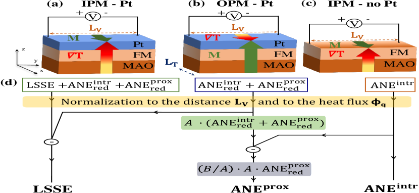
Figures 1(a)-(c) illustrate the measurement geometries that we have employed for the separation of the three effects. In the IPM geometries (Figs. 1(a),(c)) the application of an out-of-plane temperature gradient T in the presence of an in-plane magnetic field along the x-axis induces a transverse voltage along the y-axis. While measuring in this IPM configuration with Pt on top (IPM - Pt, Fig. 1(a)) we detect the LSSE voltage together with both ANE contributions, intrinsic and proximity-induced. However, in the IPM geometry without Pt (IPM - no Pt, Fig. 1(c)) we are only sensitive to the intrinsic ANE contribution.
The LSSE voltage is determined according to the relation
| (1) |
where , , , and denote the electric field induced by ISHE, the SSE coefficient, the spin current which enters the spin detector material and the spin polarization vector, respectively. Moreover, the ANE contribution is described by the relation
| (2) |
where , , and denote the electric field induced by ANE, the ANE coefficient, and the magnetization vector of the FM, respectively.
In the OPM geometry with Pt on top (OPM - Pt, Fig. 1(b)), the application of an in-plane temperature gradient T together with an out-of-plane magnetic field generates a transverse voltage attributed to the intrinsic and proximity-induced ANE. In this configuration, the LSSE can not be detected, since no out-of-plane spin current with the proper spin polarization direction is generated Kikkawa et al. (2013a). One major issue is to consider the reduction of the ANE signal upon a placement of a Pt layer Ramos et al. (2013). All ANE contributions measured with Pt on top have in general reduced contributions and this is indicated by the subscript “red” in Fig. 1 and throughout the whole manuscript.
Figure 1(d) explains the flow chart for the quantitative disentanglement of the three effects. As a first step, the electric field is calculated from the measured voltages by normalizing to the distance of the electric contacts . Then, this electric field is divided by the heat flux that runs through the sample. The normalization to the heat flux as suggested by Sola et al Sola et al. (2015, 2017), allows eliminating the systematic errors due to the thermal surface resistances and thermal contacts resulting in the effective comparison between IPM and OPM configurations as well as in the comparability of our results. Further details on the heat flux normalization can be found in the Supplemental Materials III Bougiatioti et al. (including Refs. Schulz and Hoffmann (2002); Nelson et al. (2014)). To estimate the ANE reduction due to the additional Pt layer we used the ratio of conductances of the NiFe2O and the Pt in a parallel arrangement Ramos et al. (2013)
| (3) |
with : RT resistivity and : thickness of the corresponding layer. The reduced intrinsic ANE signal (ANE) from the OPM - Pt configuration is then corrected by the factor Ramos et al. (2013) resulting in the pure ANEANE. This correction step in our calculations is highlighted by the light green area in Fig. 1(d). Combined with the information on the ANE from the IPM - no Pt configuration (cf. Fig. 1(c)), i.e., by subtracting the ANE from the corrected term, this method already yields a qualitative criterion for the existence or absence of proximity-induced ANE in the sample.
For a quantitative evaluation, an additional correction has to be applied to the reduced proximity-induced ANE signal (ANE) due to the additional non-magnetic Pt layer, while the correction on the term has to be reversed (see light grey area in Fig. 1(d)).
The correction factor for the ANE is given by Ramos et al. (2013), where and are the thicknesses of the spin polarized Pt layer and the non-magnetic fraction, respectively, estimated by XRMR. Then, the corrected proximity-induced ANE contribution is denoted as ANEANE. For the polarized and unpolarized fraction of the Pt layers, the same resistivity was used.
Exemplarily, for the Pt/Ni33Fe67 (Pt/NiFe2O) sample the reduction of the ANE is estimated to be 47 (95) by using the measured values for the RT resistivity of Pt equal to = for a Pt film with thickness nm (3.1 nm) and of the FM equal to = for a FM thickness of = 10.4 nm (35 nm). Moreover, for the metallic Pt/Ni33Fe67 bilayer the reduction of the ANE is estimated to be 71 by considering nm spin polarized layer of Pt and nm of non-magnetic Pt. A table with the obtained values for all samples can be found in the Supplemental Materials IV Bougiatioti et al. . Consequently, the comparison between the voltage signals in the IPM and OPM geometries enables a quantitative separation of the parasitic ANE contributions from the LSSE signal.
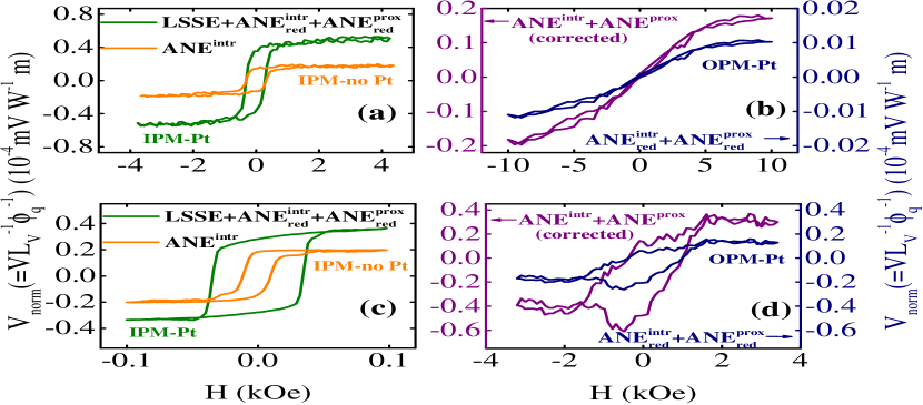
Figure 2 illustrates the experimental results for the Pt/NiFe2O and Pt/Ni33Fe67 bilayers. For Pt/NiFe2O (Fig. 2(a)), the LSSE is the most prominent contribution to the total voltage signal, while for Pt on metallic Ni33Fe67, the intrinsic ANE and the LSSE are of comparable magnitude (Fig. 2(c)). By comparing the difference between the ANE from the IPM - no Pt configuration and the ANE + ANE signals (corrected ANE + ANE by and , as explained above) we are able to quantitatively determine the contribution from the proximity-induced ANE. For the non-metallic NiFe2O bilayer (Fig. 2(a),(b)) no difference can be determined between the saturation values of the ANE data from IPM - no Pt configuration (orange line in Fig. 2(a)) and the saturation values of the ANE + ANE signal (corrected OPM - Pt data, purple line in Fig. 2(b)), which are extracted to be V in both cases. Thus, the ANE is zero and can be neglected for this sample. On the contrary, for the Pt/Ni33Fe67 bilayer (Fig. 2(c),(d)) the ANE + ANE is larger than the ANE signal unveiling the existence of MPE. Furthermore, for the Pt/NFO bilayer both ANE and ANE + ANE signals are zero confirming the absence of any ANE contribution in the pure Pt/NFO bilayer Kuschel et al. (2015, 2016).
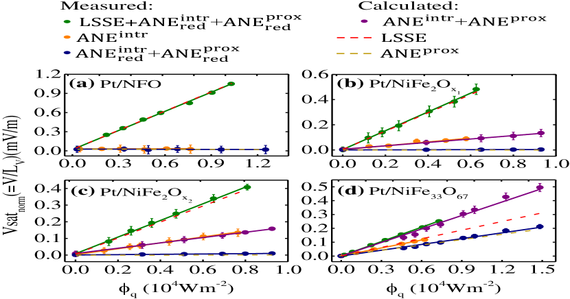
Figure 3 illustrates the linear dependence of the voltage in saturation on , normalized to for all samples. The dashed lines are the calculated contributions of the pure LSSE and ANE extracted as described in the diagram of Fig. 1(d) after correcting the reduced ANE signal arising from both the FM and the spin polarized Pt layer. In Fig. 3(a), the zero line contribution of both types of ANE indicates the absence of MPE in Pt/NFO bilayers Kuschel et al. (2015, 2016). The low amount of mobile charge carriers in the nearly-insulating NFO leads to a vanishing ANE contribution Meier et al. (2013).
As shown in Figs. 3(a)-(c), the LSSE contribution is dominant for all Pt/NiFe2O () bilayers that consist of oxides. Furthermore, the absence of any proximity-induced ANE is verified, since no difference between the ANE and the ANE + ANE can be identified. Additionally, for the Pt/NiFe2O bilayer the ANE contribution is 14 larger than for the Pt/NiFe2O bilayer pointing towards its more conducting character. For the Pt/Ni33Fe67 bilayer (Fig. 3(d)), the enhancement of ANE + ANE due to the metallic character of Ni33Fe67 and the MPE contribution is clearly displayed.
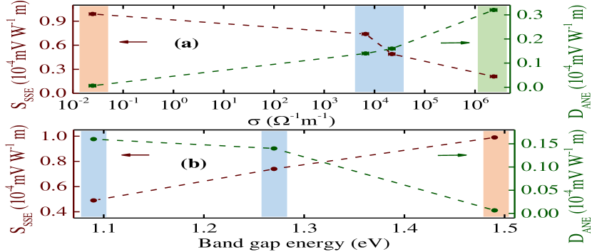
Figure 4(a) shows the SSE () and ANE () coefficients extracted from the corresponding slopes of the curves in Fig. 3, plotted against the RT value for the measured electrical conductivity. There is a pronounced increase of the when the conductivity increases, whereas the decreases.
Figure 4(b) depicts the dependence of the SSE and ANE coefficients on the optical band gap for the NFO and NiFe2O bilayers. A short description of the band gab determination can be found in the Supplemental Materials V Bougiatioti et al. (including Refs. Meinert and Reiss (2014); Bougiatioti et al. (2017); Lord and Parker (1960); Klewe et al. (2014); Meier et al. (2013)). It is clearly observed that the more conducting samples are characterized by lower band gap energies, reflecting the existence of additional electronic states in the band gap. Additionally, the ANE coefficient increases for decreasing band gap energy verifying the previous assumption of more mobile charge carriers at a reduced oxygen concentration. On the contrary, the SSE coefficient increases for larger band gap energies.
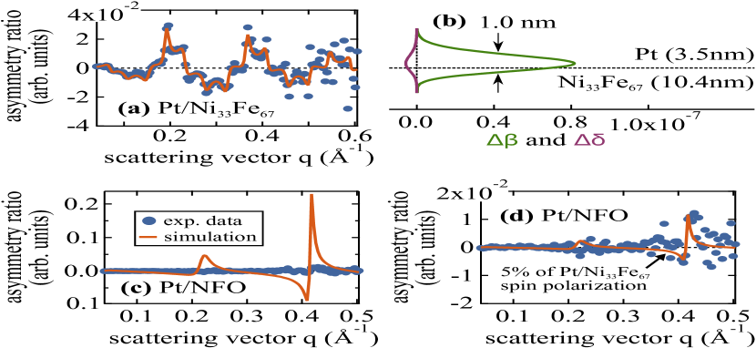
The absence of MPE in Pt/NFO, Pt/NiFe2O samples and the presence of MPE in the metallic Pt/Ni33Fe67 bilayer is now confirmed by XRMR (Fig. 5). In Fig. 5(a) the measured XRMR asymmetry ratio for the Pt/Ni33Fe67 bilayer is displayed. From the corresponding fitting and by comparing the experimental fit values of and derived from the magnetooptic depth profile in Fig. 5(b) to ab initio calculations Kuschel et al. (2015), we obtain a maximum Pt magnetic moment of per spin polarized Pt atom, consistent with earlier results Klewe et al. (2016). The effective spin polarized Pt thickness is calculated to be nm similar to our previous investigations Klewe et al. (2016).
In Fig. 5(c) the measured XRMR asymmetry ratio for the Pt/NFO bilayer is presented along with a simulation using a magnetooptic depth profile identical to the one derived for the Pt/Ni33Fe67 bilayer. Obviously, the simulated asymmetry ratio of the Pt/NFO sample (Fig. 5(c)) deviates strongly from the one of the Pt/Ni33Fe67 sample (Fig. 5(a)), although the same magnetooptic depth profile (Fig. 5(b)) was used. This is due to the different optical constants of Ni33Fe67 and NFO. Since no asymmetry was detected for the Pt/NFO sample, a potential MPE present in this film must be significantly smaller than in the all-metallic system.
By decreasing the magnitude of the magnetooptic parameters down to 5 of the Pt/Ni33Fe67 spin polarization (Fig. 5(d)), we can estimate a detection limit leading to an upper limit for the maximum magnetic moment in Pt of 0.04 per spin polarized Pt atom. Moreover, for the Pt/NiFe2O and Pt/NiFe2O samples a detection limit of 0.1 and 0.01 per spin polarized Pt atom is extracted in the same way, see Supplemental Materials II Bougiatioti et al. . Finally, possible MPEs can be neglected down to these limits for all samples except for the metallic Pt/Ni33Fe67 bilayer, where a distinct spin polarization in the Pt layer can be observed.
In conclusion, we investigated thermal spin transport phenomena in Pt/FM bilayers and separated the intrinsic ANE in the FM and proximity-induced ANE contributions quantitatively from the LSSE for sputter-deposited NiFe2O bilayers. This new compact procedure is based on the preparation of twin samples (with and without Pt), different measurement geometries, the normalization to the heat flux instead of the thermal gradient, and the determination of important correction factors to obtain quantitative LSSE and ANE values. In our work, we extracted the dependence of the LSSE and intrinsic ANE coefficients on the band gap energy and on the electrical conductivity of the samples. Furthermore, possible static MPE in Pt were studied via XRMR. We found no magnetic response down to our detection limits of 0.04 , 0.1 and 0.01 per spin polarized Pt atom for Pt/NFO, Pt/NiFe2O and Pt/NiFe2O, respectively. For the Pt/Ni33Fe67 we calculated a maximum magnetic moment of 0.48 per spin polarized Pt atom. All XRMR results are well in line with the absence/presence of proximity-induced ANE contributions. In a next step this technique of thermal transport effect separation allows to study the individual transport effects depending on other properties of the samples, e.g., thicknesses and roughnesses. Even the proximity-induced thermal magnetotransport can be extracted experimentally as well as the LSSE can be identified in metallic films.
The authors gratefully acknowledge financial support by the Deutsche Forschungsgemeinschaft (DFG) within the Priority Program Spin Caloric Transport (SPP 1538) and the European Synchrotron Radiation Facility (ESRF). Christoph Klewe further acknowledges financial support by the Alexander von Humboldt foundation.
References
- Hoffmann and Bader (2015) A. Hoffmann and S. D. Bader, Phys. Rev. Applied 4, 047001 (2015).
- Bauer et al. (2012) G. E. W. Bauer, E. Saitoh, and B. J. van Wees, Nat. Mater. 11, 391 (2012).
- Hirsch (1999) J. E. Hirsch, Phys. Rev. Lett. 83, 1834 (1999).
- Uchida et al. (2010) K. Uchida, H. Adachi, T. Ota, H. Nakayama, S. Maekawa, and E. Saitoh, Appl. Phys. Lett. 97, 172505 (2010).
- Uchida et al. (2014) K. Uchida, M. Ishida, T. Kikkawa, A. Kirihara, T. Murakami, and E. Saitoh, J. Phys.: Condens. Matter 26, 343202 (2014).
- Liu et al. (2011) L. Liu, T. Moriyama, D. C. Ralph, and R. A. Buhrman, Phys. Rev. Lett. 106, 036601 (2011).
- Liu et al. (2012) L. Liu, C.-F. Pai, Y. Li, H. Tseng, D. Ralph, and R. Buhrman, Science 336, 555 (2012).
- Tang et al. (2013) Z. Tang, Y. Kitamura, E. Shikoh, Y. Ando, T. Shinjo, and M. Shiraishi, Appl. Phys. Express 6, 083001 (2013).
- Pai et al. (2012) C.-F. Pai, L. Liu, Y. Li, H. W. Tseng, D. C. Ralph, and R. A. Buhrman, Appl. Phys. Lett. 101, 122404 (2012).
- Saitoh et al. (2006) E. Saitoh, M. Ueda, H. Miyajima, and G. Tatara, Appl. Phys. Lett. 88, 182509 (2006).
- Stoner (1938) E. C. Stoner, Proc. R. Soc. London Ser. A 165, 372 (1938).
- Huang et al. (2012) S. Y. Huang, X. Fan, D. Qu, Y. P. Chen, W. G. Wang, J. Wu, T. Y. Chen, J. Q. Xiao, and C. L. Chien, Phys. Rev. Lett. 109, 107204 (2012).
- Meier et al. (2013) D. Meier, T. Kuschel, L. Shen, A. Gupta, T. Kikkawa, K. Uchida, E. Saitoh, J.-M. Schmalhorst, and G. Reiss, Phys. Rev. B 87, 054421 (2013).
- Ramos et al. (2013) R. Ramos, T. Kikkawa, K. Uchida, H. Adachi, I. Lucas, M. H. Aguirre, P. Algarabel, L. Morellón, S. Maekawa, E. Saitoh, and M. R. Ibarra, Appl. Phys. Lett. 102, 072413 (2013).
- Ramos et al. (2014) R. Ramos, M. H. Aguirre, A. Anadón, J. Blasco, I. Lucas, K. Uchida, P. A. Algarabel, L. Morellón, E. Saitoh, and M. R. Ibarra, Phys. Rev. B 90, 054422 (2014).
- Ramos et al. (2015) R. Ramos, T. Kikkawa, M. H. Aguirre, I. Lucas, A. Anadón, T. Oyake, K. Uchida, H. Adachi, J. Shiomi, P. A. Algarabel, L. Morellón, S. Maekawa, E. Saitoh, and M. R. Ibarra, Phys. Rev. B 92, 220407 (2015).
- Ramos et al. (2016) R. Ramos, A. Anadón, I. Lucas, K. Uchida, P. A. Algarabel, L. Morellón, M. H. Aguirre, E. Saitoh, and M. R. Ibarra, APL Mater. 4, 104802 (2016).
- Wu et al. (2014) S. M. Wu, J. Hoffman, J. E. Pearson, and A. Bhattacharya, Appl. Phys. Lett. 105, 092409 (2014).
- Lee et al. (2015) K.-D. Lee, D.-J. Kim, H. Y. Lee, S.-H. Kim, J.-H. Lee, K.-M. Lee, J.-R. Jeong, K.-S. Lee, H.-S. Song, J.-W. Sohn, S.-C. Shin, and B.-G. Park, Sci. Rep. 5, 10249 (2015).
- Uchida et al. (2015) K. Uchida, T. Kikkawa, T. Seki, T. Oyake, J. Shiomi, Z. Qiu, K. Takanashi, and E. Saitoh, Phys. Rev. B 92, 094414 (2015).
- Uchida et al. (2016) K. Uchida, H. Adachi, T. Kikkawa, A. Kirihara, M. Ishida, S. Yorozu, S. Maekawa, and E. Saitoh, Proc. IEEE 104, 1946 (2016).
- (22) Bauer et al. Bauer et al. (2012) introduced the term “spin Seebeck effect” for FMI systems while for the spin-dependent thermal creation of moving electrons in metals and semiconductors they suggested the term “spin-dependent Seebeck effect” (SDSE). In our letter we will not distinguish between SSE and SDSE in the conducting materials and, thus, we just use the term SSE throughout the letter .
- Kikkawa et al. (2013a) T. Kikkawa, K. Uchida, Y. Shiomi, Z. Qiu, D. Hou, D. Tian, H. Nakayama, X.-F. Jin, and E. Saitoh, Phys. Rev. Lett. 110, 067207 (2013a).
- Xu et al. (2014) Y. Xu, B. Yang, C. Tang, Z. Jiang, M. Schneider, R. Whig, and J. Shi, Appl. Phys. Lett. 105, 242404 (2014).
- Miao et al. (2016) B. F. Miao, S. Y. Huang, D. Qu, and C. L. Chien, AIP Adv. 6, 015018 (2016).
- Kikkawa et al. (2013b) T. Kikkawa, K. Uchida, S. Daimon, Y. Shiomi, H. Adachi, Z. Qiu, D. Hou, X.-F. Jin, S. Maekawa, and E. Saitoh, Phys. Rev. B 88, 214403 (2013b).
- Macke and Goering (2014) S. Macke and E. Goering, J. Phys.: Condens. Matter 26, 363201 (2014).
- Kuschel et al. (2015) T. Kuschel, C. Klewe, J.-M. Schmalhorst, F. Bertram, O. Kuschel, T. Schemme, J. Wollschläger, S. Francoual, J. Strempfer, A. Gupta, M. Meinert, G. Götz, D. Meier, and G. Reiss, Phys. Rev. Lett. 115, 097401 (2015).
- Brown et al. (2001) S. D. Brown, L. Bouchenoire, D. Bowyer, J. Kervin, D. Laundy, M. J. Longfield, D. Mannix, D. F. Paul, A. Stunault, P. Thompson, M. J. Cooper, C. A. Lucas, and W. G. Stirling, J. Synchrotron Radiat. 8, 1172 (2001).
- (30) P. Bougiatioti, C. Klewe, D. Meier, O. Manos, O. Kuschel, J. Wollschläger, L. Bouchenoire, S. D. Brown, J.-M. Schmalhorst, G. Reiss, and T. Kuschel, Supplemental Materials .
- Bouchenoire et al. (2003) L. Bouchenoire, S. D. Brown, P. Thompson, J. A. Duffy, J. W. Taylor, and M. J. Cooper, J. Synchrotron Radiat. 10, 172 (2003).
- Klewe et al. (2014) C. Klewe, M. Meinert, A. Boehnke, K. Kuepper, E. Arenholz, A. Gupta, J.-M. Schmalhorst, T. Kuschel, and G. Reiss, J. Appl. Phys. 115, 123903 (2014).
- Sola et al. (2015) A. Sola, M. Kuepferling, V. Basso, M. Pasquale, T. Kikkawa, K. Uchida, and E. Saitoh, J. Appl. Phys. 117, 17C510 (2015).
- Sola et al. (2017) A. Sola, P. Bougiatioti, M. Kuepferling, D. Meier, G. Reiss, M. Pasquale, T. Kuschel, and V. Basso, arXiv:1701.03285 (2017).
- Schulz and Hoffmann (2002) B. Schulz and M. Hoffmann, High Temp. - High Pressures 34, 203 (2002).
- Nelson et al. (2014) A. T. Nelson, J. T. White, D. A. Andersson, J. A. Aguiar, K. J. McClellan, D. D. Byler, M. P. Short, and C. R. Stanek, J. Am. Ceram. Soc. 97, 1559 (2014).
- Kuschel et al. (2016) T. Kuschel, C. Klewe, P. Bougiatioti, O. Kuschel, J. Wollschläger, L. Bouchenoire, S. D. Brown, J. M. Schmalhorst, D. Meier, and G. Reiss, IEEE Trans. Magn. 52, 4500104 (2016).
- Meinert and Reiss (2014) M. Meinert and G. Reiss, J. Phys.: Condens. Matter 26, 115503 (2014).
- Bougiatioti et al. (2017) P. Bougiatioti, O. Manos, C. Klewe, D. Meier, J.-M. Schmalhorst, T. Kuschel, and G. Reiss, in preparation (2017).
- Lord and Parker (1960) H. Lord and R. Parker, Nature 188, 929 (1960).
- Klewe et al. (2016) C. Klewe, T. Kuschel, J.-M. Schmalhorst, F. Bertram, O. Kuschel, J. Wollschläger, J. Strempfer, M. Meinert, and G. Reiss, Phys. Rev. B 93, 214440 (2016).