A Large Ungated TPC with GEM Amplification
Abstract
A Time Projection Chamber (TPC) is an ideal device for the detection of charged particle tracks in a large volume covering a solid angle of almost . The high density of hits on a given particle track facilitates the task of pattern recognition in a high-occupancy environment and in addition provides particle identification by measuring the specific energy loss for each track. For these reasons, TPCs with Multiwire Proportional Chamber (MWPC) amplification have been and are widely used in experiments recording heavy-ion collisions. A significant drawback, however, is the large dead time of the order of per event generated by the use of a gating grid, which is mandatory to prevent ions created in the amplification region from drifting back into the drift volume, where they would severely distort the drift path of subsequent tracks. For experiments with higher event rates this concept of a conventional TPC operating with a triggered gating grid can therefore not be applied without a significant loss of data. A continuous readout of the signals is the more appropriate way of operation. This, however, constitutes a change of paradigm with considerable challenges to be met concerning the amplification region, the design and bandwidth of the readout electronics, and the data handling. A mandatory prerequisite for such an operation is a sufficiently good suppression of the ion backflow from the avalanche region, which otherwise limits the tracking and particle identification capabilities of such a detector. Gas Electron Multipliers (GEM) are a promising candidate to combine excellent spatial resolution with an intrinsic suppression of ions. In this paper we describe the design, construction and the commissioning of a large TPC with GEM amplification and without gating grid (GEM-TPC). The design requirements have driven innovations in the construction of a light-weight field-cage, a supporting media flange, the GEM amplification and the readout system, which are presented in this paper. We further describe the support infrastructure such as gas, cooling and slow control. Finally, we report on the operation of the GEM-TPC in the FOPI experiment, and describe the calibration procedures which are applied to achieve the design performance of the device.
keywords:
Gas Electron Multiplier (GEM) , Time Projection Chamber (TPC) , Particle tracking , Particle identification , Ion backflow , FOPI , ALICE1 Introduction
A gas-filled Time Projection Chamber (TPC) [1] with its low material budget, large solid-angle coverage and excellent pattern recognition capabilities is an ideal detector for three-dimensional tracking and identification of charged particles. TPCs have been already used in many experiments such as PEP-4 [2], ALEPH [3], DELPHI [4], NA49 [5, 6], and are currently being employed e.g. in STAR [7, 8] and ALICE [9]. In a conventional TPC, electron-ion pairs created by an ionizing particle within the drift volume are separated by an electric field. Electrons drift towards the readout anode, where they produce a charge avalanche in Multiwire Proportional Chambers (MWPCs) [10] which induces a detectable signal in the cathode pads. In order to prevent the ions produced in the avalanche from drifting back into the drift volume of the TPC, where they would severely distort the drift field, a switchable electrostatic gate must be employed. This, however, inevitably leads to dead times and limits the TPC readout rate to values of the order of few .
In order to efficiently employ TPCs in experiments with high interaction rates, new techniques of ion-backflow suppression have to be found which do not require the use of a gating grid. Gas Electron Multiplier (GEM) foils [11] represent an optimal solution since they offer an intrinsic suppression of the ion backflow [12]. A GEM consists of a thin insulating polyimide foil with copper-coated surfaces, typically thick. The foil is perforated by photolithography and etching processes, forming a dense, regular hexagonal pattern of holes. In the standard geometry the holes have a double-conical shape with an inner diameter of , an outer diameter of , and a pitch of . Figure 1 shows an electron microscope image of a standard GEM foil.
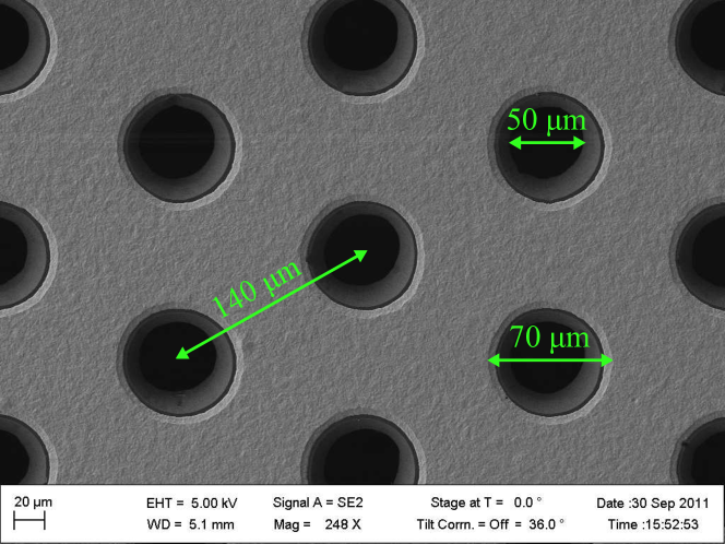
The small dimensions of the amplification structures lead to very large electric fields inside the holes of the GEM foil of the order of if a moderate voltage difference of (depending on the gas) is applied between the metal layers. Such fields are sufficient to create an avalanche inside the hole of the GEM foil. Avalanche electrons are extracted from the hole by the electric field applied below the GEM foil and can be further multiplied in subsequent GEM foils or collected at the anode. Detectors based on a triple-GEM amplification have been pioneered by the COMPASS experiment at CERN [13, 14, 15, 16], and are now routinely used in several particle physics experiments like LHCb [17], PHENIX [18], and TOTEM [19]. New applications include the use of GEM-based detectors in KLOE-2 [20] and CMS [21].
Owing to their small diffusion, the ions created in the avalanche inside a GEM hole closely follow the electric field lines leading to the top side of the GEM foil and are collected there. Depending on the electric field settings, only a fraction of the ions created in the avalanche drifts back into the drift volume. This mechanism of ion backflow suppression is illustrated in Fig. 2.
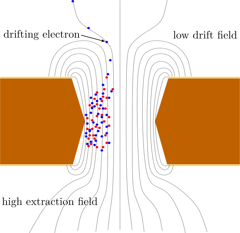
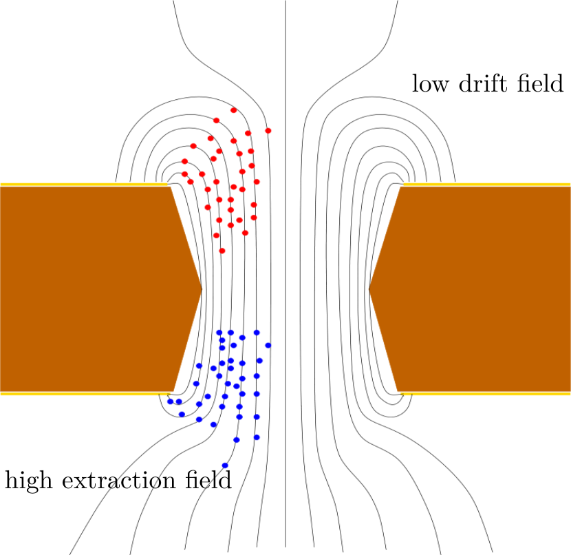
Although the ion suppression in a multi-GEM stack is of the order of to a few and hence does not reach the same level as a gating grid (see e.g. [22, 23] for a summary of the present status of ion backflow measurements), the resulting track distortions due to ion backflow are limited to a few , and can thus be corrected using advanced calibration techniques. This provides the possibility to operate a TPC without the gating grid in a continuous, trigger-less mode, allowing an increase in event rate by two orders of magnitude, as foreseen e.g. in ALICE at CERN [24, 25].
In order to prove the concept of an ungated TPC with GEM amplification the detector presented in this paper was built. The GEM-TPC was commissioned with cosmic rays and with particle beams at the FOPI experiment at GSI in Darmstadt (Germany), and was employed for an experimental campaign with a secondary pion beam. This paper describes the design and construction of the GEM-TPC including the auxiliary systems which were custom-made for this detector. Section 2 gives a general overview of the design of the GEM-TPC. In section 3 the electro-mechanical design of the field-cage is presented, followed in section 4 by a detailed description of the so-called media flange, which hosts all supply connections and is the central support element of the detector. The GEM amplification stage is described in section 5, the pad-plane with hexagonal-shaped signal pads in section 6. The front-end electronics and the data acquisition system are discussed in section 7. Section 8 describes the cooling system for the front-end electronics, while the gas system and chosen gas mixture are presented in section 9. The slow control system used to operate the GEM-TPC detector is treated in section 10. Finally, in section 11 the results from the commissioning in the FOPI experiment are presented followed in section 12 by a discussion of the calibration procedures applied in order to reach the design performance of the GEM-TPC.
2 General Design
The GEM-TPC presented in this paper has a cylindrical shape with the two end-planes serving as cathode and anode, respectively, and an inner bore for the beam. The key parameters of the GEM-TPC are listed in Table 1.
| Parameter | Value | Unit | |
|---|---|---|---|
| Outer Dimensions: | |||
| Inner Diameter | 104 | ||
| Outer Diameter | 309 | ||
| Total Length | 843 | ||
| Active Volume: | |||
| Inner Diameter | 110.2 | ||
| Outer Diameter | 299.0 | ||
| Drift Length | 727.8 | ||
| Gas Volume | 48 | ||
| GEM amplification stage: | |||
| Effective gain | |||
| GEM thickness | |||
| GEM pitch | |||
| GEM hole Ø | |||
| Transfer gaps | 2 | ||
| Induction gap | 4 | ||
| Electronics | |||
| No. of readout pads | 10,254 | ||
| ASIC | AFTER (T2K) | ||
| Sampling clock | |||
| Buffer depth | 511 | samples | |
| Dynamic range | 120 | ||
| No. of front-end cards | 42 | ||
| ADC resolution | 11 | bit | |
| Sensitivity | 393 | ||
| Average ENC | 720 | ||
The outer diameter of the TPC was chosen to fit inside the Central Drift Chamber (CDC) of FOPI (see section 11) while the inner diameter was chosen to host different target dimensions. The dimensions also match the requirements for the Crystal Barrel experiment at ELSA [26], so that a similar detector could be used as a tracking system in this experiment in the future.
The design of the detector takes into account the fixed-target nature of the FOPI experiment, with the ionization electrons drifting in one direction only, different from the symmetric setup with a central cathode and two anodes as used in collider experiments. The cathode is oriented in the forward direction with respect to the beam, while the readout anode and the associated readout electronics are situated in the backward region in order to minimize the material exposed to particles emitted in interactions with the target, which is mounted in the inner bore.
The detection gas is enclosed in a vessel formed by two concentric cylinders and the two end planes. In addition to containing the detector gas, this vessel also serves as field cage to realize the required uniform electric field parallel to the cylinder axis. In order to keep the multiple scattering and interactions of traversing particles as low as possible a very thin but rigid composite material is used for the field-cage. On the cathode side the field-cage vessel is closed by an end plate of similar sandwich structure as the field cage.
On the anode side a rigid flange called media flange is glued to the field-cage. The media flange is used to fix the detector to external structures and houses all the connections for gas supply, high voltage, low voltage and sensor read-out. Two further flanges are mounted to the upstream side of the media flange: the GEM flange housing the GEM stack, and the read-out flange holding the pad-plane, which is patterned with hexagonal pads for a two-dimensional localization of the incoming charge. The printed circuit boards holding the front-end (FE) electronics are directly connected to the back side of the pad-plane in a fan-shaped arrangement and are supported by two rigid rings made of Aluminum. These flanges are fixed to the media flange by external metal clamp bands and are sealed by rubber O-rings. Figure 3 and Fig. 4 show a cross-section and a photo of the final large GEM-TPC, respectively.
The whole apparatus is therefore composed of three mechanically separable parts: the field-cage cylindrical vessel with the media flange, the GEM flange and the read-out flange. This modular setup allows an easy maintenance of the detector system and to supply and read out the GEM-TPC exclusively from the anode side.
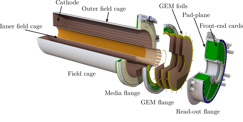
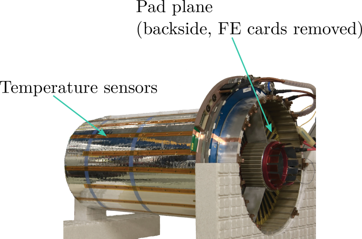
The GEM-TPC was mounted inside the existing FOPI spectrometer at GSI [27] and employed in experimental campaigns with hadron and secondary pion beams at intermediate energies of few . One major innovation in this TPC is the construction of a light-weight field-cage (section 3) with a material budget below of a radiation length. This keeps the multiple scattering in front of the other sub-detectors small to prevent a deterioration of their tracking performance. The target position is chosen such that most of the produced particles are emitted in the forward direction, where the material budget of the TPC is lowest, while all the rigid support structures as well as the all infrastructure connections are located upstream of the target position. Since the overall center of gravity of the TPC is close to the detector backward end-cap, only few fixation points at the media flange are necessary to hold the GEM-TPC in place. Another major achievement within this project is the adaption of the T2K AFTER chip (section 7) for the specific needs of the GEM-TPC.
3 Field-cage
3.1 General Concept
Owing to physical and mechanical constraints, the cylindrical vessel of the TPC has to fulfill several requirements: it has to serve as gas container and field-cage at the same time, provide shielding of the HV to the outside while keeping the amount of material in forward and radial directions at the minimum. The main purpose of the integrated gas vessel and the field-cage is to define an electrostatic field with a relative homogeneity better than inside the gas volume to prevent that field inhomogeneities effect the detector resolution [9]. These requirements can be fulfilled employing a layered composite material. Because of its dual purpose realisation, the field-cage walls must be gas-tight and mechanically stable against changes in gas pressure and temperature. A temperature stability within should be achieved during the system operation. The vessel should furthermore withstand a potential difference of about between cathode and anode and must be electrically insulated.
3.2 Technical Realisation
3.2.1 Composite Material
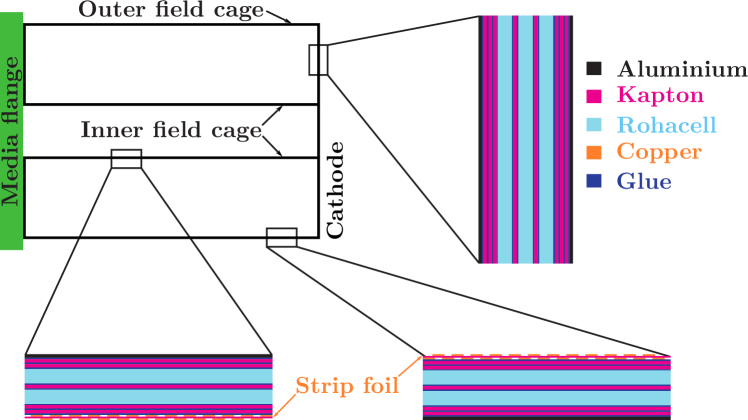
The materials, the thicknesses of the different layers that
compose the barrel walls and the cathode end-cap expressed in
and in units of a radiation length are listed in the
tables Table 2(a) and Table 2(b), respectively. The
layer stacking is sketched schematically in
Fig. 5. One can see that the layout of the two
concentric cylinders building the barrel walls and the cathode end-cap
differ slightly. The cathode end-cap is composed of three
Rohacell®
layers to stabilize the structure and a further aluminized
Kapton® foil
is added to the side facing the gas volume to realize the cathode
plane.
The barrel and the cathode end-cap are joined together by gluing the extremities as shown in Fig. 6.

| Thickness | ||
|---|---|---|
| Material | () | (X0) |
| Copper | ||
| Kapton | ||
| Copper | ||
| Kapton | ||
| Kapton | ||
| Rohacell | ||
| Kapton | ||
| Rohacell | ||
| Kapton | ||
| Kapton | ||
| Aluminium | ||
| Epoxy glue tot. | ||
| Barrel Walls | ||
| Thickness | ||
|---|---|---|
| Material | () | (X0) |
| Aluminium | ||
| Kapton | ||
| Kapton | ||
| Kapton | ||
| Rohacell | ||
| Kapton | ||
| Rohacell | ||
| Kapton | ||
| Rohacell | ||
| Kapton | ||
| Kapton | ||
| Kapton | ||
| Aluminium | ||
| Epoxy glue tot. | ||
| Cathode End-Cap | ||
Special moulds were developed and constructed for the assembly of the
cylindrical sandwich structures.
The moulds are built by panelling an Aluminium cylinder with vacuum
grooves with Metapor® slabs which are
then milled into a cylindrical
form. The outer strip foil or the inner strip foil are rolled around
the respective mould and fixed by aspirating air through the porous
Metapor material. The different
materials are then glued successively
on top of the previous layer. Vacuum bags are used to apply pressure
and to flatten the layers during the gluing procedure of the sandwich
structure. The vessel is electrically insulated by an additional
Aluminium-coated Kapton layer of placed on its
outside surface. This layer is connected to the detector-ground
potential providing a shielded Faraday cage. Two gas supply lines and
one HV line are attached to the outer field-cage parallel to the
cylinder axis. The two gas lines are connected to the gas inlet
realized with a Vespel® block hosting
two inner channels. The block
is inserted inside a cutout of the interface between the cathode and
the field-cage to allow the gas flow through the channels into the
cylinder.
The high voltage supply cable is pierced through the field-cage and
soldered onto a copper strip which in turn is glued with conductive
adhesive onto the cathode.
The thickness of the field-cage vessel in units of a radiation length
was evaluated within the Root analysis framework
[28]. A detailed geometry of the large GEM-TPC was
created and the thickness was evaluated along tracks with different
emission angles. The emission point for the considered particle
tracks was placed on the central axis of the GEM-TPC at a distance of
upstream of the cathode
plane (see Fig. 40). The obtained polar-angle
dependence of the thickness in units
of a radiation length is shown in Fig. 7.
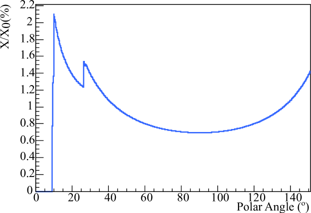
At polar angles of particles start to hit the inner field-cage wall in forward direction, causing a sharp increase of the material budget. Particles cross the cathode end plane of the field-cage up to an angle of , traversing less material of the inner barrel wall with increasing polar angle. At they start traversing both the inner and the outer barrel walls, which have a shorter radiation length than the cathode (see Table 2(b)), causing an increase in the material budget. The remaining smooth structure with a minimum at reflects the thickness of the walls crossed by particles. Above a polar angle of the thickness of the field-cage increases significantly (not shown in Figure 7) due to the large material budget of the media, GEM and readout flanges. For fixed target experiments such as FOPI where most of the tracks go in forward direction this high material budget in the backward direction has no impact on the overall detector performance.
3.2.2 Strip Foil and Voltage Divider
The layers of the inner and outer field-cage cylinders facing the gas
volume are composed of thick foils of
Kapton and
FR4, respectively.
Both foils are coated with copper on both sides.
Both copper surfaces are patterned in sets of parallel strips aligned
transversally to the beam axis and staggered between the two sides in
order to improve the homogeneity of the field. This way, 968
concentric cylindrical rings of copper with a width of and
a pitch of cover the walls of the drift volume along the
inner and outer radius, respectively. By connecting the strips with
resistors a stepwise degrading potential is obtained, from the
cathode value being about to the potential of the
last strip, close to the first GEM foil, with about
.
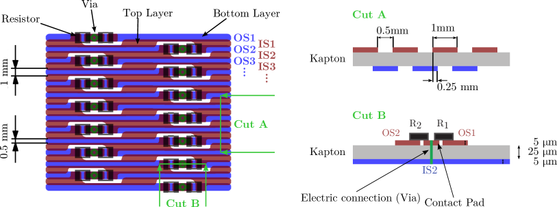
Figure 8 shows a schematic view of the strip arrangement. The top view shown on the left panel of Fig. 8 indicates in red the outer strips which are facing outwards with respect to the gas volume and have special soldering pads to allow for the connection between neighbouring strips through resistors.

The right panel of Fig. 8 shows schematic
cross-sections of the strip foil. In Cut B the top of the Kapton
foil with the two soldering pads of the neighbouring outer strips OS1
and OS2 are shown together with the contact pad placed between the two
outer strips. The contact pad is directly connected to the inner
strip IS2. The electric connection across the
thick Kapton foil is represented by the green line and green circle in
the right and left panel of Fig. 8, respectively.
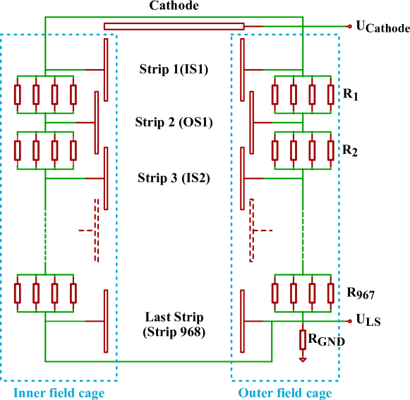
By placing the resistor between OS1 and the contact pad one connects OS1 to IS2 and by placing a second resistor one connects IS2 to OS2.
This way, all the 968 copper strips can be connected to build a
resistor chain. Sequential connections are staggered to avoid contact
between the resistors. Figure 9 shows the
scheme of the resistor chain. Only half of the symmetric
cross-section of the barrel is shown. and
represent the cathode and the last strip
potential, respectively. One can see that the end of the resistor
chain is connected to a high voltage power supply. This allows not
only to decouple the field-cage high voltage from the high voltage of
the GEM amplification system but also to vary the potential of the
last strip.
This enables to adjust the electric field between the last strip and the first GEM foil in order to minimize the distortions at the junction between the field-cage and the first GEM foil.
Since the power supply used is not able to sink currents, a resistor
of connected to ground is placed
between the power supply output and the last strip.
This ensures a positive current output for the high voltage supply.
Each of the individual 0805 SMD resistors has a
precision specification of . The resistors were
measured by hand and four elements were grouped in parallel such that
the precision of the total resistance per step could be increased to
the
needed value of . The total resistance between two
adjacent strips is then .
This results in a total resistance of
over the resistor chain for the inner and outer
cylinder, respectively.
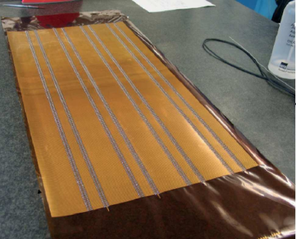
Figure 11 shows a photograph of the entire
strip-foil of the inner field-cage. One can see the 8 rows of
resistors resulting from the parallel connection and the staggering
connecting the inner to the outer strips.
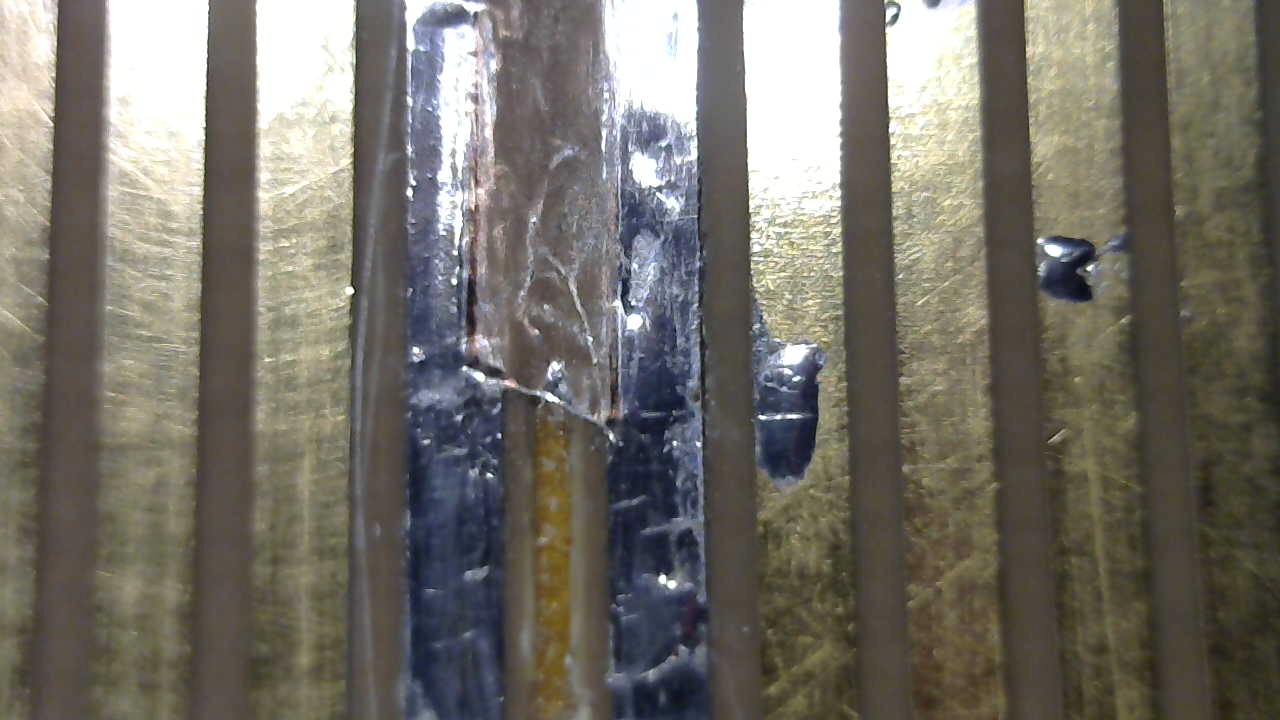
Figure 11 shows an enlarged version of the
previous image where the outer strips and the soldered resistors are
visible. Due to the limitation of the maximal width of the FR4 base
material to , the outer strip-foil is assembled by
splicing two FR4 foils together where the splicing runs in parallel to
the strips of the field-cage. Since the two spliced foils have to be
electrically connected a copper bridge is soldered in between these
two foils. This interconnection can be seen in
Figure 12.
A finite-element simulation of the GEM-TPC field-cage was carried out
to investigate the homogeneity of the drift field. A two dimensional
geometry has been used exploiting the rotational symmetry of the
GEM-TPC and different settings of the potentials have been considered
to emulate the ideal and the real setup.
The resulting field distortions within the drift volume were
evaluated.
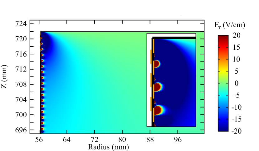
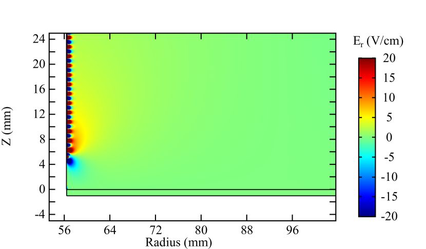
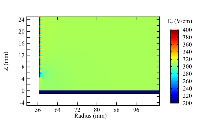
Figures 13-16 show the
simulated two-dimensional maps of the electric field for the ideal and
real setups, respectively. The color code shows the values of the
radial and the
longitudinal electric field components, respectively, for the
different settings.
The ideal set-up corresponds to the mechanical specifications given
so-far and to the following voltage settings for the cathode, last
strip and top side of the first GEM foil:
,
and
. These settings lead to a
longitudinal electric field of in the center
of the drift volume. Figure 13 shows the radial
and longitudinal components of the electric field close to the cathode
for the ideal case; the left panel shows also a schematic
representation of the first three strips close to the cathode.
Figure 14 shows the two field components close to the
last strip for the ideal settings.
Despite these expected local variations of the field close to the
field-defining structures, the required field homogeneity of
is reached at a maximal distance of from the
field cage walls, corresponding to of the total gas volume,
provided that the mechanical specifications are met.
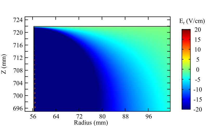
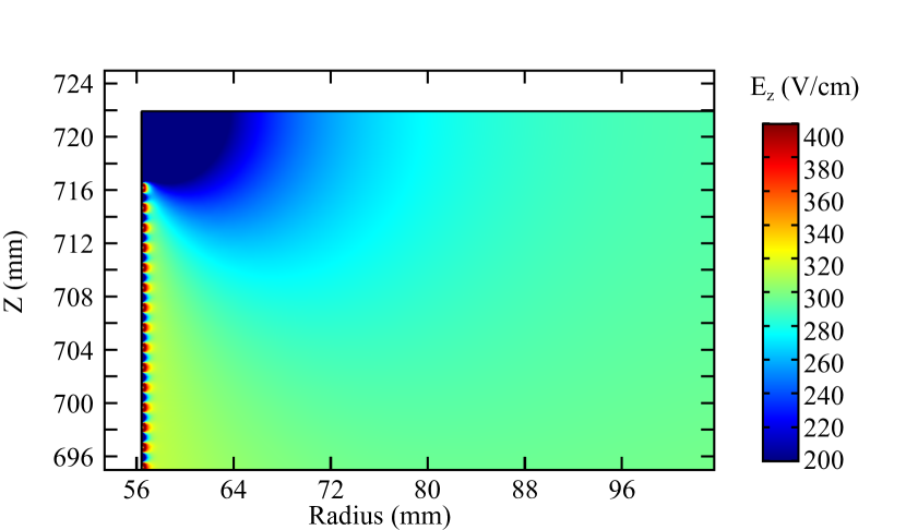
The connection of the first strip to the cathode is realised via conductive glue; during the construction of the field-cage, however, the first three strips on the outer and the first four strips on the inner cage were short-circuited by accident and are therefore at the same potential as the cathode. This configuration modifies the field close to the cathode surface as shown in Fig. 15, where the same quantities as in Fig. 13 are presented for the real setup. Moreover, during the detector commissioning too low a voltage was set to the last strip: , and . These settings lead to a longitudinal electric field of in the center of the drift volume, which is very similar to the ideal setting, but also to an additional radial component of the electric field close to the last strip and the first GEM foil as one can see in Fig. 16.
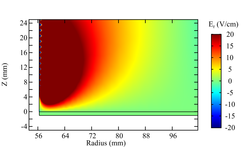
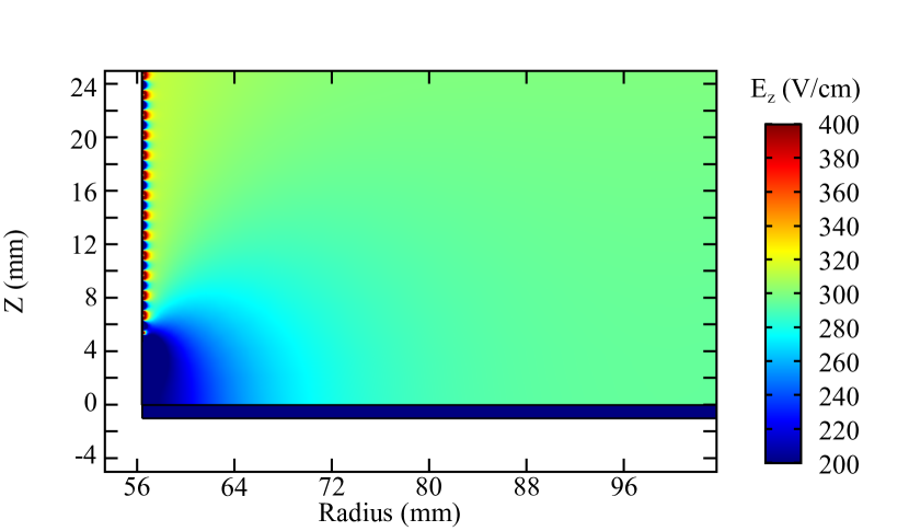
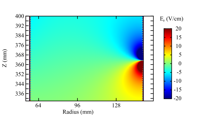
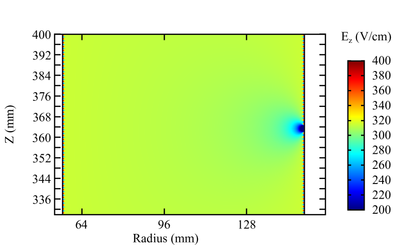
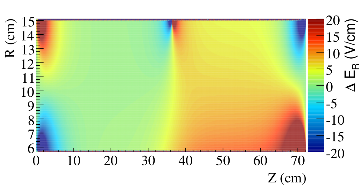
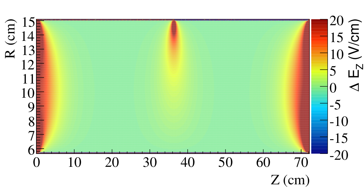
The copper bridge used to connect the two spliced foils of the outer strip foil introduces further field distortions as shown in Figure 17. There panels a) and b) show the introduced distortions in the radial component and along the -direction of the electric field, respectively. These distortions are calculated with the ideal setting mentioned above. The resulting distortions at the copper bridge for the real setting are not shown as they do not differ from the ideal setting.
The deviation of the drift field obtained for the real setup are summarized in Fig. 18. Panel a) of Fig. 18 shows the deviation from zero of the radial component of the electric field as a function of the radius and the position and panel b) presents the deviation of the -component of the electric field from the nominal value as a function of the same spatial coordinates.
4 Media Flange
The media flange is a rigid support flange which is glued to the field-cage vessel. It provides mechanical stability and serves as a mounting structure for the whole detector, is the main support for the GEM and readout flanges and provides the interfaces for all external supplies like gas, high voltage and sensors for measuring gas flow, temperature and pressure. Figure 19 displays a photo of the media flange glued onto the field-cage vessel.
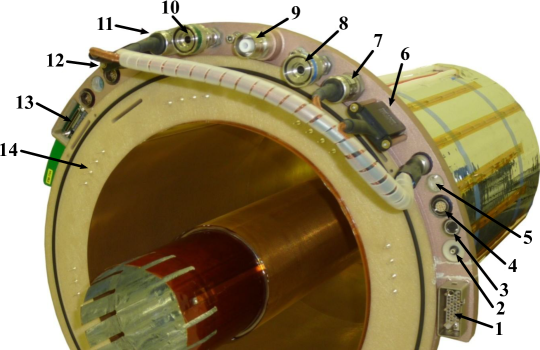
It is made of two pieces glued together in order to create internal
channels which are used for the distribution of the gas.
The main material used in the fabrication of the media flange is
Stesalit 1011. The gas in- and outlets are realized by quick coupling
connectors, type Swagelok Instrumentation Quick-Connect QC4. The high
voltage for the drift cathode is supplied via a Radiall socket, type
R341018. The high voltages for the GEM electrodes (6 channels) and
the last strip of the field-cage are supplied via a multi-pin REDEL
socket, type SLG.H51. The GEM high voltage channels are distributed
through the media flange via pins to the GEM flange (see
section 5). The last strip channel is connected within the
media flange to the outer field-cage and via an external cable to the
inner field-cage.
An additional cable connects the inner field-cage via the resistor
( in Fig. 9) to ground.
To measure the pressure at the gas inlet and outlet, two compact
pressure transducers, type Measurement Specialties M5141, are mounted
on the media flange. They are suited for measuring the pressure in
the range from . Additionally, there are two
Sensirion ASF 1400 mass flow meters, installed in series with the
inlet and outlet gas channel.
All sensor signals are read out by the GEM-TPC Slow Control system, described in section 10.
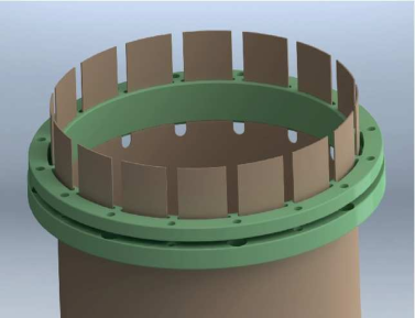
In order to fix the inner field-cage to the readout flange, it ends on
the anode side with Kapton flaps that are used to connect it to a
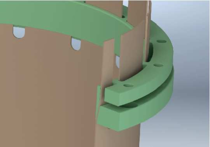
two-piece support ring. Figure 20 shows how the
flaps are inserted into the slotted holes of the upper support ring.
The two parts of the support ring are screwed together clamping the
flaps in between them. Finally, the whole structure is screwed to the
mounting system for the FE cards. By adjusting the longitudinal
position of the ring the tension and therefore the rigidity of the
inner field-cage can be controlled.
5 The GEM Amplification Stage
5.1 GEM Design, Framing and Implementation
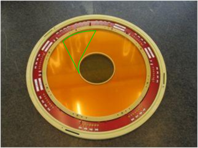
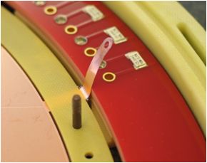
The GEMs are designed to fit to the dimensions of the GEM-TPC, so that the inner and outer radii of the GEM active area match the inner and outer radius of the TPC field cage, respectively. This results in an active area of the GEM foil of around . One side of each GEM foil is divided into eight sectors to decrease the capacitance of each sector reducing significantly the discharge probability as well as the amount of stored charge which has to be dissipated in the case of a discharge [29]. This segmentation furthermore allows an operation of the TPC even in case of several non-operational sectors per foil. The eight sectors are shaped like aperture blades (see Fig. 21 a) and are separated by thick insulating borders where the copper layer was etched away. Each sector has a flap on the outer radius to connect it to the high voltage distribution board located inside the GEM flange (see Fig. 21 b). The high voltage distribution board also contains bias resistors for each sector.
As the distance between two GEM foils or a GEM foil and the read-out
anode determines the field strength, a well defined and constant
spacing throughout the whole foil has to be maintained. This is
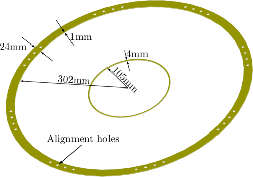
achieved by gluing thick FR4 frames onto each side of a
foil while applying tension to the foil.
The frames and their dimensions are depicted in Fig. 22.
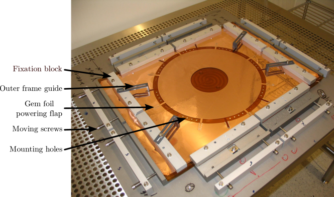
The foil is stretched by applying tension on the four sides of the
uncut rectangular foil. To this end, the foil edges are clamped
between two fixation blocks
where the lower one is movable and has a silicone rubber inlay to
provide the necessary friction. The upper block fixes the edge to the
lower block. By
moving the fixation blocks with the help of screws, the foil can be
stretched until no wrinkles are left. Figure 23
shows an uncut foil mounted
inside the stretching tool and stretched via the fixation blocks.
When the GEM foil is completely flat the inner and outer FR4 rings are glued on the upper side of the GEM foil with Araldite AW106 (hardener: 953U). Alignment holes are distributed along the outer circumference of the GEM foil and on the outer FR4 frame. The alignment holes on the outer GEM frame are visible in Fig. 22. The outer ring is aligned by placing pins through the alignment holes of the frames and the GEM foils into holes on the metal plate underneath the foil. A special tool employing the same alignment pins as for the outer ring is used for the deployment of the inner ring. This tool is basically a metal plate with concentric groves for the two frames which holds the inner frame with the help of a small air pump. This metal plate additionally serves as a weight to apply pressure on both rings while curing the glue. The glue is cured for about ten hours at a temperature of around .
In the next step the foil is flipped and the whole procedure is repeated for the other side of the GEM foil. After the stretching and framing procedure is completed the unnecessary material around the outer frame is removed. The framed GEM foils are then permanently under tension and flat and can be assembled into a stack fixed to the GEM flange. Before, during and after the gluing high voltage tests of the GEM foils are performed to ensure the functionality and high voltage stability. To perform these tests, the foil is set under nitrogen atmosphere and voltages up to are applied to each sector via a bias resistor, while all remaing sectors as well as the un-sectorized side are grounded. The ramping scheme and the dwell time for each HV step are listed in Table 3.
| Voltage () | Dwell time |
|---|---|
| Until currents are stable | |
| Until currents are stable | |
| Until currents are stable | |
| Until currents are stable | |
In Fig. 21 one can see a framed GEM mounted in the GEM flange.
The GEM flange can hold up to four GEM foils which are rotated with respect to each other to allow for a proper mounting of the flaps to the HV distribution. The positioning of the framed GEM foils is realized with alignment pins. Finally, the flaps of each sector are connected to their corresponding high voltage pin on the distribution board, visible in red in Fig. 21, which is also mounted inside the GEM flange. The unsegmented side of a GEM foil is connected with just one flap to the high voltage distribution board. Pins connect the high voltage distribution board to the media flange where a Redel connector (Fig. 19(1)) is placed to connect the GEM-TPC to the high voltage module. The frames with their thickness of define the spacing in-between two GEM foils as shown in Fig. 24.
5.2 GEM HV scheme
For the sake of flexibility, we chose an HV supply for the GEM stack which includes a separate HV channel for each side of a GEM foil. On the one hand, operation with a resistor chain is known to be more reliable and stable because it avoids by design that large potential differences build up between electrodes in case of a trip of a single sector or in case of different time constants of discharging the foils. On the other hand, it is not possible in this configuration to test different voltage settings, which was an important asset for the present detector.
In the nominal configuration, the three GEM foils in a stack are mounted with the sectorized side facing the drift region [13]. Each sector is powered through a separate bias resistor (=, Fig. 25) in order to limit the current in case of a discharge. The upper limit of is determined by the fact that the voltage drop across the GEM due to charge produced in the detector should remain small, such that the gain is not affected by the particle rate. The unsectorized side of a foil does not have a bias resistor, but is connected directly to the power supply. This configuration has the virtue of fixing the potential at the bottom side of each GEM to its nominal value in case of a discharge, thus avoiding excessive potential differences to the next stage or to the readout anode and effectively preventing discharges from propagating to the next stage. In addition, such a scheme allows for an operation of the detector even in case of permanent short circuits in several sectors. For a TPC, however, such a scheme is not directly applicable, because, at least for the top GEM directly facing the drift volume, the homogeneity of the drift field would be severely distorted by one sector at a potential which is different from the others. Therefore, at least the top GEM has to be mounted with the sectorized side facing the anode. The other foils should be mounted in the standard orientation, as shown in Fig. 24.
Due to an error in the design, however, a flipping of the GEM foils is not possible for the detector described in this paper. Therefore, all foils have to be mounted with the sectorized side facing the anode. To limit the increase of the potential on the lower side of the GEM in case of a discharge, a bias resistor is mounted also for the unsectorized side (). The resulting configuration, which is shown schematically in Fig. 25, puts additional constraints onto the operational scheme, which has to be coped with during the operation: (i) needs to be increased when a short circuit appears (switches in Fig. 25) because of the additional voltage drop over , which limits the numbers of bad sectors due to the voltage limit of the power supply. (ii) In case of a high particle rate, the resulting current produced in the detector leads to a larger voltage drop over and than for the nominal configuration with only . Each GEM foil is powered by two independent channels of an ISEG EHS 8060n high voltage module. In case of a shortcut sector the voltage drop over the grounding resistor prevents currents from flowing into the high voltage supply.
In conclusion, the adopted power supply scheme, although flexible, turned out to be not the optimal choice, and for stable operation at fixed settings should be replaced by a simple voltage divider (possibly exchangeable if flexibility is needed), or a stack of floating power supplies.

6 The Pad-Plane
The charge cloud emerging from the last GEM induces a negative, fast electron signal on the readout pads. For single incoming electrons, the FWHM of the induced signal is of the order of , depending on the transverse diffusion between the GEM stages and the spread inside the GEM holes. Consequently, a pitch of the readout elements of the same order of magnitude would be required to profit from a center-of-gravity reconstruction. For a TPC, however, transverse diffusion of the ionization electrons during their drift to the amplification stage will dominate the precision with which its original position can be reconstructed, except for very small drift distances. The pad size should then be chosen such that the transverse diffusion for a given gas mixture and magnetic field dominates the resolution, and not the pad size. Furthermore the geometrical configuration of the pads should prevent a deterioration of the spatial resolution of the tracks due to angular effects.The pad-plane used for this GEM-TPC is designed following these guiding principles.
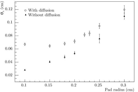
For a uniform charge distribution independent of the crossing angle of tracks, pads with a hexagonal shape are chosen. The optimum outer pad radius () was determined to be with the help of Monte Carlo simulations assuming a Ne/CO2 (90/10) gas mixture and a magnetic field of , as originally foreseen for the TPC of the PANDA experiment. The definition of the pad radius is depicted in Figure 26 in the left panel. The gaps between the pads are wide. As one can see in Figure 27 these simulations show that the spatial resolution and hence the momentum resolution does not improve for outer radii of the hexagonal pads below , as diffusion in the drift volume is the dominant contribution to the localization accuracy.

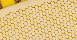
The pad-plane is realized as a printed circuit board (PCB) made of FR4 with thick gold-plated Cu pads. Figure 26 (b) shows a photographic image of the pad-plane, which in total has readout pads. Since the pad-plane is also used to close the gas volume it had to be designed in a gas-tight way. This is done by using a four-layer PCB with signal tracks on all layers and staggered connections between neighboring layers. On the backside of the pad-plane the signal lines are routed to 42 high-density connectors (Samtec BTH-150-01-F-D-A) with 300 pins and a pitch of each. The connectors are arranged radially.
To avoid crosstalk between different pads the connections from the pads to the connectors are designed to minimize crossing of tracks or narrow parallel tracks of neighboring pads. Field inhomogeneities on the outer part of the pad-plane are avoided by placing copper areas, matching the shape of the pads, as shown in Fig. 26 (b). Further details about the construction of the pad-plane can be found in [30].
7 Front-end Electronics and Data Acquisition
7.1 General Requirements
The current signal
seen by the charge-sensitive amplifier (CSA) connected to a readout pad is
determined by
the convolution of two distributions. The first is the
ionization-charge
distribution along the drift direction at the moment when it reaches
the GEM foils. The spread of the charge is caused by the longitudinal
diffusion of electrons during their drift through the TPC gas
volume. The second is the shape of the current pulse induced by
electrons drifting from the last GEM electrode to the readout pad,
which has a negative polarity with a fast risetime
and a duration of about . The length of the convoluted signal
depends on the drift length. For the GEM-TPC considered here it is
about on average.
The CSA is followed
by a shaper with a programmable peaking time between and
for optimization of the signal-to-noise ratio and the
effect of pile-up.
The sampling rate has to be adapted to the shaper output and should
thus be chosen between and .
A crucial parameter for a continuously operating TPC is the noise
level of the readout system, which has to be
as low as possible () in order to operate the chamber at
the minimum possible gain, defined by the required
signal-to-noise ratio. A low gain in turn minimizes the ion backflow
and the resulting track distortions.
To allow for a continuous readout of the TPC, the front-end chip has
to be able to simultaneously sample the incoming data and transfer
the processed data to the next stage.
Power consumption should be minimized to a level of
to avoid the necessity of
excessive cooling of the front-end cards.
Last but not
least, the chip has to be highly integrated to match the channel
density on the pad plane.
The SAMPA chip
[31] which is currently being developed for the upgrade
of the ALICE TPC will fulfill all of the above requirements. At the
time of the design and construction of the GEM-TPC no chip
that matched all these requirements was available. The
AFTER T2K chip [32] was chosen as a good compromise
because it fulfils the low noise, low power consumption and high
integration requirements. It
does not allow, however, on-chip zero suppression and to concurrently
sample and transfer the data.
7.2 The AFTER ASIC
The AFTER chip is a low-noise, low-consumption analog pipeline ASIC developed for the T2K near detector TPCs and fabricated in CMOS technology [33]. It has 76 channels, of which 72 are connected to input pins, each with a tunable preamplifier/shaper followed by a 511-cell switched capacitor array (SCA) analog memory. In Fig. 28 a simplified functional diagram of a single channel of the AFTER ASIC is shown.
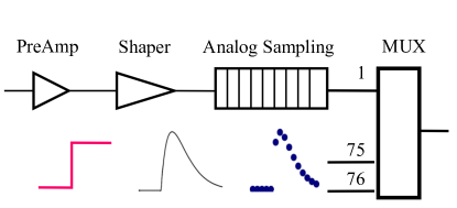
The main parameters of the AFTER ASIC can be found in Table 4.
| Parameter | Value |
|---|---|
| Number of input channels | 72 |
| Samples per channel | 511 |
| Noise (nominal) | 500 at |
| Dynamic range | (4 values) |
| Peaking time | to (16 values) |
| Sampling frequency | |
| Readout frequency | |
| Power Consumption | |
| Size of the package |
The preamplifier charge range can be chosen to be
from . The shaper has an adjustable
peaking time in the range from to
. After the shaper the signals are sampled
into an analog buffer which is implemented as two SCAs, each with 36
channels, and a depth of 511 samples. Each
of the SCAs has two internal channels not connected to the input which
can be used to correct for common mode noise and so-called fixed
pattern noise due to
charge loss in the capacitors (SCA-leakage). The sampling clock is
supplied externally and can range from .
All the tunable parameters
of the chip can be accessed via a custom serial slow
control protocol.
Upon a trigger the content of the SCA is multiplexed to a differential
line at
a frequency of , time slice by time slice starting
from the oldest sample. The full reading cycle takes during
which writing is disabled, which poses the main rate limitation of
this chip.
7.3 Front-end card
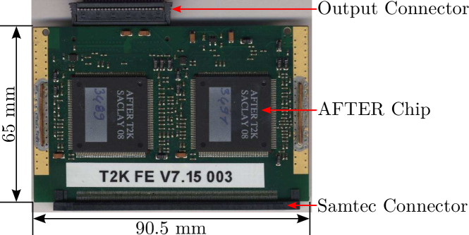
One front-end card (Fig. 29) houses four AFTER-chips and is directly connected to the pad plane via a 300-pin connector (SAMTEC BSH-EM-150) mounted sideways. Only 64 channels of the available 72 per chip are connected to the pad plane, such that one front-end card reads out a total of 256 detector channels. All four chips are controlled and read out in parallel. The total power consumption per card is . As the TPC is very sensitive to temperature variations, heat transfer from the front-end cards to the gas volume is avoided by dissipating the excessive heat with an active water-driven cooling system (see section 8). Figure 29 shows a photograph of a front-end card. Detector channels 1 – 32 are connected to the pins on the far side of the Samtec connector and thus have longer signal paths than detector channel 33 – 64, which are connected to the pins facing the Samtec connector (see also Fig. 45 in section 12.2).
7.4 Readout Chain
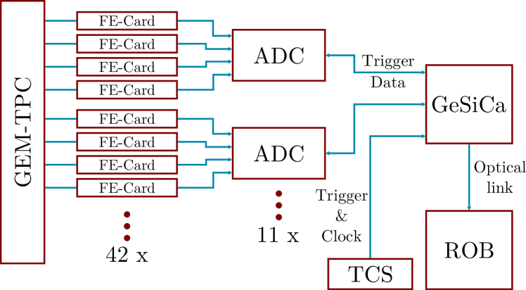
For the read-out, the scheme developed for the COMPASS experiment [34] at CERN has been adapted for the GEM-TPC. The read-out scheme is displayed in Figure 30. Clock () and trigger signals are sent via optical fibers from the Trigger Control System (TCS) to readout driver modules (so-called GeSiCA) and from there they are distributed to the ADC modules. From there, each AFTER ASIC is supplied with two clock signals derived from the TCS clock: WRITE_CLK, which defines the sampling frequency and which is configurable as an integer division of a , and READ_CLK, which defines the data readout to the ADC and which is fixed to half the TCS clock (). During the commissioning phase (cf. section 11, the detector was operated at an average trigger rate of , determined mainly by the dead time needed to read out the buffer of the AFTER chip (cf. section 7.2). Upon arrival of a trigger signal the AFTER chips read the values stored in the SCAs and multiplex them via a differential line to the ADC modules. One ADC module can handle the data from up to four front-end cards (16 AFTER chips). The analogue signals from the AFTER ASICs are sampled by pipelined ADCs with a sampling rate matching the readout clock of the AFTER ASIC. A Xilinx Virtex-4 FPGA on the ADC board performs online baseline subtraction and zero suppression of the digitized data. The zero suppression algorithm takes into account individual thresholds on each channel, calculated from the measured noise performance of the channels (see Sec. 12.2). To correct for the fixed pattern noise in the AFTER chip another correction algorithm has been implemented. For each channel of one SCA the mean of the two unconnected channels is subtracted to correct for the charge loss in the capacitors. After processing the data of 16 chips in the ADC module they are sent via an optical fiber to the GeSiCA module. One GeSiCA module can combine data from up to seven ADC modules and transmit these sub-events via an optical link to a read-out buffer at a maximum speed of . The read-out buffer performs the final event building for the TPC and stores the data to a hard drive or sends it via TCP/IP to other computers for further processing. In total 42 front-end cards (168 AFTER chips) are used to read out the 10,254 channels of the GEM-TPC. This leads to a required number of 11 ADC and 2 GeSiCa modules. The total raw data size at the input of the ADC modules amounts to and corresponds to a data rate of at a trigger rate of . After zero suppression in the ADC modules, the total data rate is reduced to , depending on the occupancy and the duty cycle of the beam. For the experiment with a pion beam (cf. section 11), the average occupancy was with a duty cycle of , while for the tests with heavy-ion beams the occupancy was about 4 to 6 times higher with a similar duty cycle.
7.5 Gain Calibration of the AFTER-ADC System
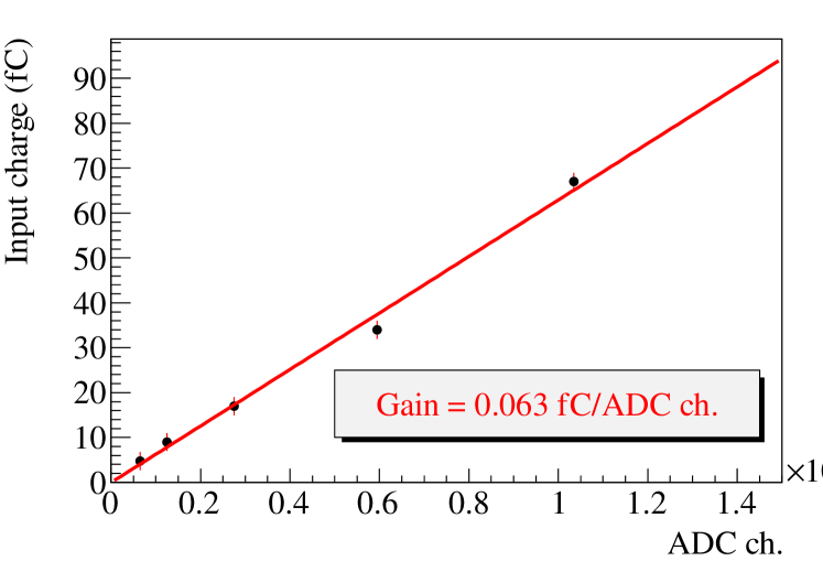
The conversion gain of the system AFTER + ADC has been measured by injecting a known charge into a pin of the AFTER chip via a SMD capacitor soldered to a readout pad of the pad plane. Several different amplitudes of a step-like input pulse have been used as shown in Fig. 31. The conversion gain derived from a linear fit is , or .
8 Cooling
With power consumption per channel a total of created by all front-end cards has to be dissipated.
Since the cards are directly plugged to the backside of the readout plane without a thermal barrier, it is important to actively cool the cards in order to avoid heat being introduced into the gas volume via the pad-plane, which would cause local variations of the drift velocity.
In addition, cooling is needed for the ADC modules in order to avoid overheating of electronic components installed in regions without air convection.
Both systems are cooled using a closed circuit water-driven cooling
system operated at overpressure and connected to a chiller (Huber
Kältemaschinen UC080T-H Umwälzkühler [35]).
The latter provides a coolant temperature of .
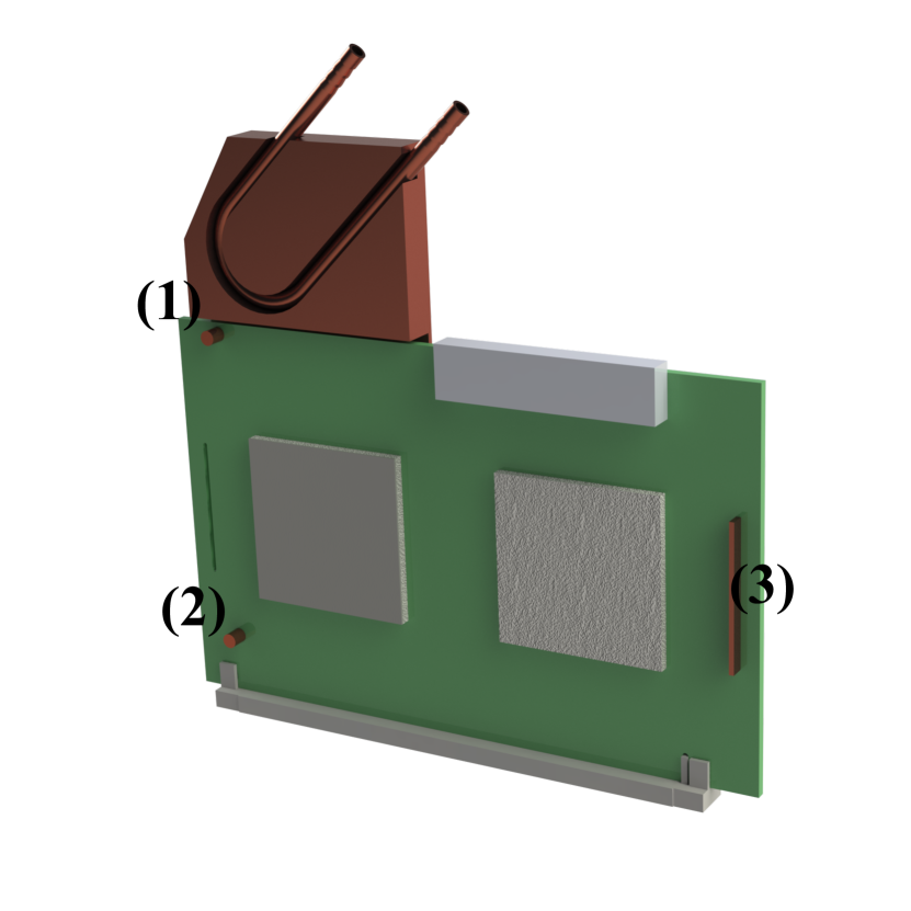
Each FE card is sandwiched between two copper plates put in direct contact with the four FE chips through heat conducting pads.
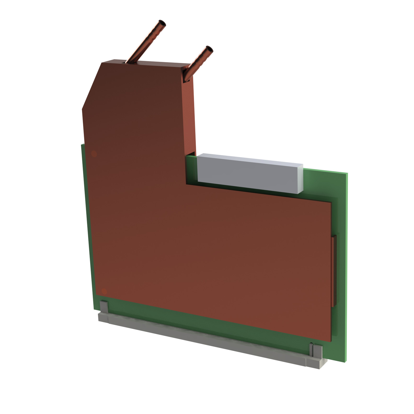
The copper plates in turn are in contact with a heat exchanger connected to the cooling water circuit.
The FE cards are shown in Fig. 32 with the heat-conducting pads attached to the housing of the FE chips shown in panel a) and with the copper plates attached to the pads as in panel b).
The copper plates are mounted by soldering them at three positions 1-3 indicated in Fig. 32, panel a).
The two pins (1-2 in Fig. 32, panel a)) are only soldered to the copper plates while the metal bar (3 in Fig. 32, panel a)) is also soldered to the PCB.
The heat exchanger is mounted by three screws to the copper plates.
This way, the heat exchanger can be removed and this allows for an easy mounting of the FE cards.
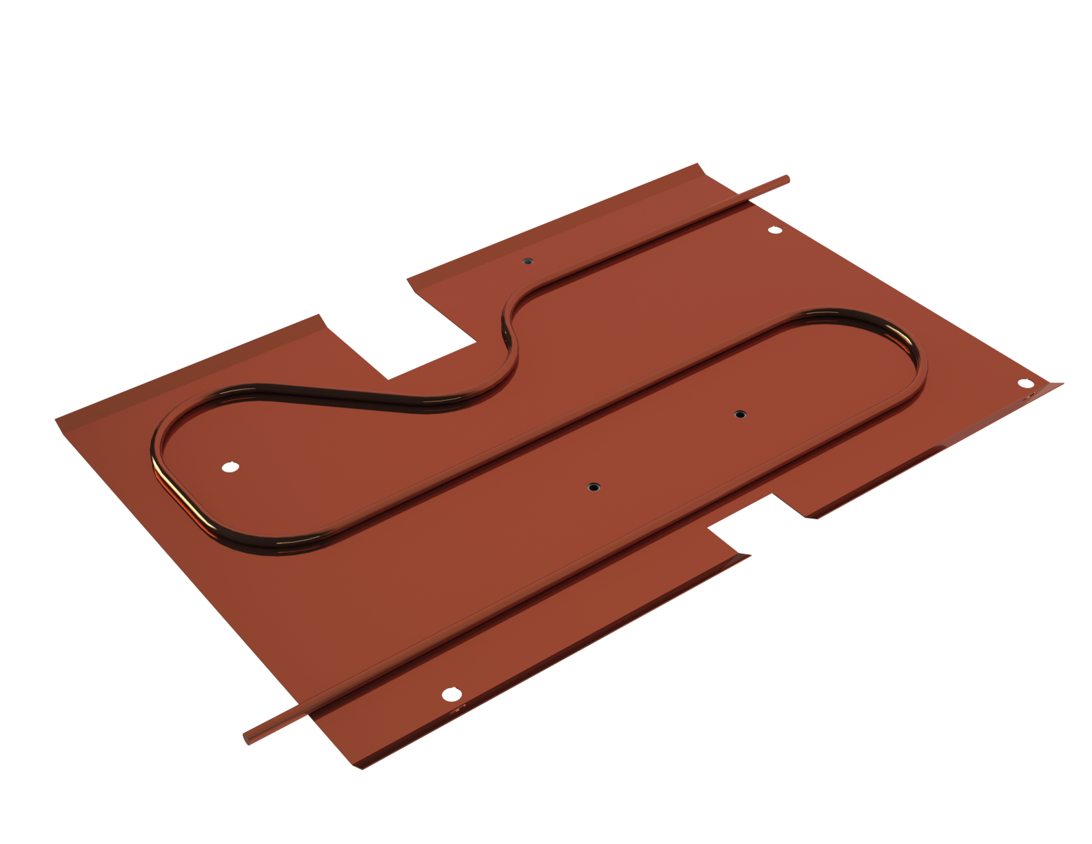
The pipe for the cooling water is soldered into a groove in the copper block and has an outer diameter of and a wall thickness of .
Since 42 FE cards have to be cooled at the same time, a homogeneous flow of cooling water through all heat exchangers has to be guaranteed.
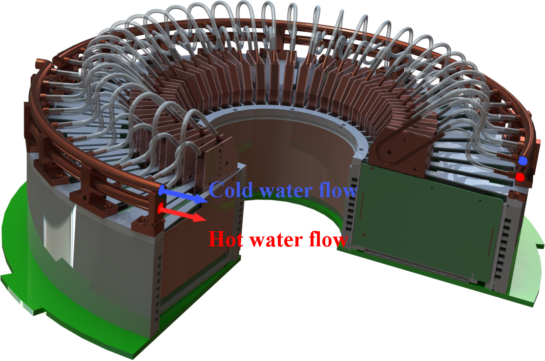
This was achieved by attaching inlets and outlets, one pair for each FE card, to the supply line such that the flow resistance is the same through all heat exchangers.
The scheme in Fig. 33 shows how this is realized.
One can see that the path length and therefore the flow resistance of the cooling liquid is the same for each heat exchanger.

The cooling water is distributed by two rings made out of copper pipes to allow for soldering nozzles for the connection to the FE card heat exchangers by flexible polyurethane tubes. Figure 34(a) shows a CAD rendering of the complete cooling setup as it was used for the GEM-TPC.
To validate the uniformity of the cooling, simulations were taken out in two steps. In the first step the flow of the cooling liquid including the heat exchangers but not the FE cards were simulated.
The second step was the simulation of the heat distribution in the FE cards taking the results of the first step into account.
The simulation for the first step was performed with the FEM flow simulation framework of SolidWorks.
It was found that taking into account an inlet water flow of the flow of the cooling liquid through the heat exchangers is in average with a still rather large variance of .
As mentioned above, in a second step the temperature distribution of the FE card was calculated for all 42 liquid flow values found in the previous simulation.
This calculation was carried out using the COMSOL FEM software and the model shown in Fig. 34.
Each chip introduces a power of uniformly on its surface and only heat transport by conduction through the FE card and cooling system materials is assumed.
The model was validated beforehand by a measurement showing that the maximal difference between measurement and calculation is below .
Figure 35 shows the outcome of this calculation where a flow of and a water temperature of were used for the calculation.
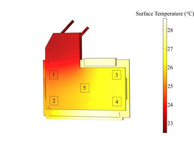
Finally, an average temperature of with a variance of measured at position 5 in Fig. 35 was found for the FE cards taking into account the various flow values from the calculation mentioned above and a water temperature of .
The same system provides the cooling of the voltage regulators of the ADCs and the ADCs themselves through a serial connection of the pipes following the cooling ring for the FE cards.
In this case, a copper sheet with an soldered pipe was attached to each ADC module (Fig. 34(b)).
In the same way as for the FE cards each chip was in thermal contact via an heat conducting pad with an aluminium block which again was screwed to the copper sheet.
The bending of the pipe in contact with the copper sheet was chosen to maximize the contact area and to cross each aluminium block.
9 Gas System
9.1 Operational Requirements
The gas system supplies the detector vessel with the drift gas mixtures Ar/CO2 (90/10) and Ne/CO2 (90/10) and with a radioactive Kr gas during calibration. In order to test different gas mixtures the system must be capable of switching between gases and modifying the mole ratio to test different quencher contributions. The system also must allow the user to change the detector gas to nitrogen during stand-by mode in order to keep the detector volume dry and oxygen-free.
One of the main requirements to the GEM-TPC gas system is the minimization of the oxygen and water vapour concentration inside the detector vessel. A contamination by an electro-negative gas as O2 leads to attachment of the primary electrons and thus to a deterioration of the spatial and d/d resolution. The water vapour reduces the effective drift field and the drift velocity since H2O molecules can be easily polarized shielding the electric field. A contamination by oxygen or water vapour can originate from badly sealed joints and permeation through the TPC wall material. For the large ALICE TPC, where the volume-to-surface ratio is about , an oxygen level lower than was reached. This value can be considered as a reference for this GEM-TPC where the volume-to-surface ratio is only . In addition to the gas purity, the accuracy and stability of the CO2 content is crucial, as it determines important parameters like the drift velocity and diffusion within the gas.
9.2 Implementation
A closed gas circulation system is employed for the GEM-TPC (see Figure 36).
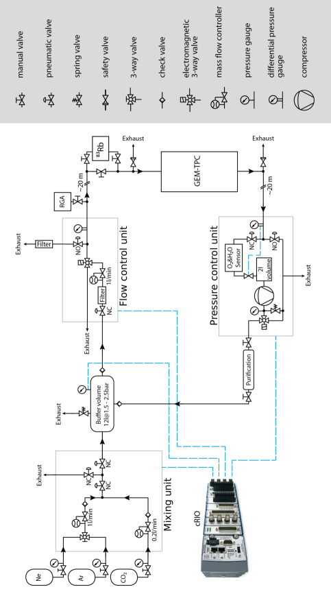
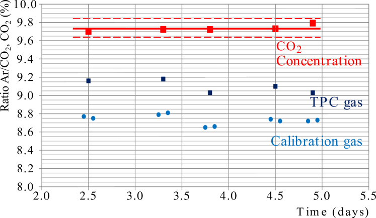
The system is composed of a mixing unit, a flow control unit, and a pressure control unit. For the mixing of the gas two SLA5850S mass flow controllers (MFC) are used. By regulating the gas flow of the individual mass flow controllers the desired mixing ratio of Ar/Ne and CO2 is achieved. The gas mixture is filled into a buffer volume which serves as a reservoir to refill the gas system if needed. During operation the pressure inside the buffer volume is kept between and . One of the outputs of the buffer volume is connected via a particle filter to the flow control unit which controls the total gas flow to the TPC. The total volume of the GEM-TPC is about and a flow rate of is used for both Ar/CO2 and Ne/CO2 gas mixtures. A differential pressure gauge is installed in the flow control unit to measure overpressure up to . A residual gas analyzer (RGA) is installed in order to monitor the gas composition after the flow control unit using a quadrupole mass spectrometer (QMS). Figure 37 shows an example of this measurement for a time interval of 2.5 days. The ratio Ar to CO2 is shown for the analyzed gas sample and a calibration sample composed of a premixed Ar/CO2 gas. The measured CO2 concentration with an error band corresponding to fluctuations is shown as well.

For calibration of the gain uniformity (see section 12.3), radioactive 83mKr can be introduced into the TPC by flushing the gas through a vessel containing 83Rb. A pressure control unit is located at the gas outlet of the TPC. This unit controls the total overpressure and measures the oxygen and water vapour content of the gas. For the oxygen measurement a Teledyne Model 3190 system with a measurement range from and a relative accuracy of was used. In Fig. LABEL:pic:gas_purity_b the oxygen content for a period of five days is shown. The mean oxygen content within this time drops slightly from to . This still rather large number is probably due to leakages in the field cage sealing but it did not lead to any significant signal losses.
To measure the water vapour content a EE375 dew point transducer was used. After leaving the pressure control unit the gas enters the purification to remove oxygen and water vapour from the gas. The oxygen is removed with activated copper by oxidizing to copper-oxide while the water vapour is removed by molecular sieves with a pore size of . The whole gas system is controlled by a National Instruments CompactRIO module which consists of:
-
1.
a NI-9265 current output module to control the set points of the MFCs,
-
2.
a NI-9203 to read the MFC output signals,
-
3.
a NI-9205 to read the outputs of the pressure gauges, the oxygen sensor and the water vapour sensor,
-
4.
a NI-9237 to read out the pressure gauge of the flow control module,
-
5.
Two NI-9485 to control the electromagnetic three-way valves.
All valves and flow MFCs were controlled by a LabView-based slow control system which also monitored and recorded all values. Further details about the gas system can be found in [36].
10 Slow Control System
For a safe detector operation it is crucial to monitor and control all parameters in a convenient and reliable way. In the case of the TPC the main parameters to be controlled are the high-voltage potentials of the cathode, the last strip, and the GEM foils and the low voltage of the front-end powering. Furthermore various temperature and pressure sensors located inside the TPC have to be monitored.
10.1 High-Voltage System
A safe operation of the TPC requires a supervision of every individual
high voltage that is applied to the GEM foils and the drift cathode.
In addition, the possibility to operate all high voltage channels
simultaneously, especially during ramping, is required. To avoid any
damages to
the chamber, a fast emergency shutdown of the high voltage system is
indispensable.
Furthermore the system should allow the configuration of this
emergency shutdown.
The high voltage system for the GEM stack requires a voltage stability
below , current measurement with a resolution of
, adjustable ramp speeds, full remote
controllability and output voltages of up to . For
the drift cathode a high voltage system with a voltage of up to
and currents up to is
needed. An ISEG EHS 8060n HV module and an ISEG HPn300, controlled by
a W-Ie-Ne-R MPOD crate were employed as this modules satisfy all
demands.
Both systems have a fast hardware based over-current trip switch with a channel-wise adjustable current limit and they can be controlled via Simple Network Management Protocol (SNMP) commands over Ethernet or directly over CAN bus.
The current architecture of an emergency high voltage shutdown system
offers two solutions. A purely hardware-based approach and a hardware
plus software approach. The hardware approach couples the HV system
of the cathode and the field-cage with the HV system of the GEM stack
by an interlock cable. In case of a trip in one of the two systems
both are shutdown immediately.
In this scenario a trip in the GEM stack also causes the drift voltage to trip and vice versa.
The long ramping time of the cathode after such a trip introduces
hereby a significant dead time of several hours. For the hardware
plus software approach the HV systems are not coupled by an interlock
cable and therefore trip independently. To minimize the the potential
danger of sustained discharges between the first GEM foil and the last
field-cage strip in case of a trip of the GEM stack, a software
adjustment of the drift cathode voltage to of the
nominal value is implemented. In case of a trip of the cathode HV no
additional actions have to be taken. Besides the trip behavior, two
additional security functions are implemented: if the measured
voltages rises above a threshold voltage or if the current steps up
unexpectedly the TPC is ramped down with to
prevent severe damages. The moving average over the last 10 values is
calculated continuously and compared with the set value. If the
deviation is larger than the limit an alarm rings.
The limit can be adjusted via the slow control interface (section 10.3) with a default value of of the set voltage of the respective channel.
To detect over-currents, the average of the last ten measured values
is compared with the average of ten values from ten seconds earlier.
Especially the currents are good indicators for a possible failure of
the detector, because any short-cut between the GEM foils or at the
field-cage will result in a sudden increase of the current. The
default for the over-current check is an increase of the current by a
factor of 1000. This value can also be configured via the slow
control interface. It has been found that this check is only
necessary during the ramping. As soon as the desired potentials are
reached the hardware over-current protection of the high voltage
modules is preferable as it is much faster.
10.2 Temperature, Pressure and Gas Flow
Various sensors are directly attached to the TPC, namely temperature sensors on the pad-plane and the outside field-cage walls and gas flow and pressure sensors. For the temperature measurement at the outer surface of the TPC 210 Dallas 18B20U 1-wire temperature sensors are used. The 12 PT100 temperature sensors located on the pad-plane are digitized by AD7998 12-Bit ADCs and read out via an Ethernet-to-I2C adapter. The ASF1400 gas flow sensor is read out via RS232 while the pressure sensor is read out by a custom-made ATMega32 based read out.
10.3 User Interface
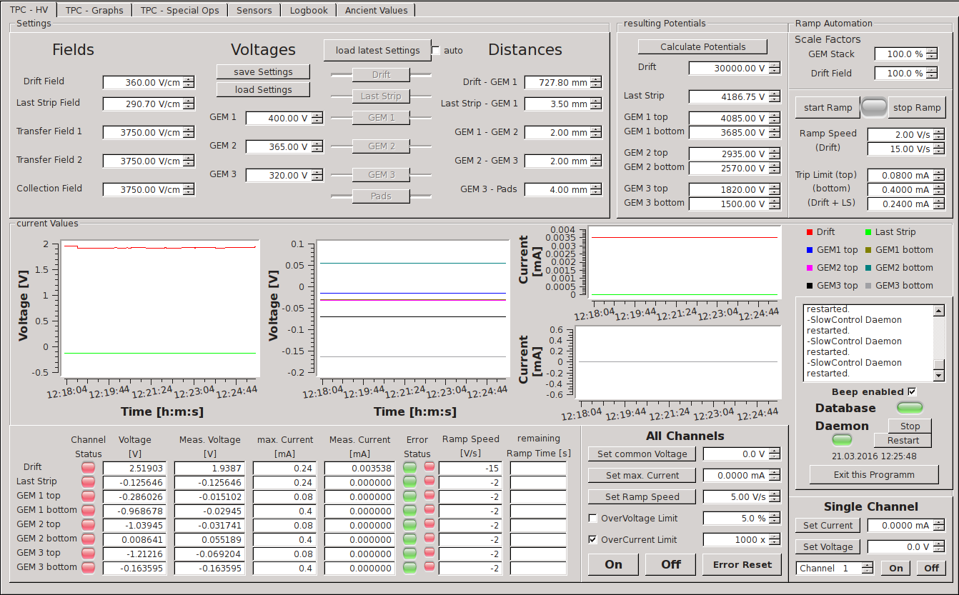
The control and read out of the high voltage modules, temperature, flow and pressure sensors is realized by a C++ based graphical user interface (GUI). In order to communicate between the GUI and the high voltage modules a background daemon is used. Additionally all data such as the actual voltages are collected by this daemon and written to a SQL based database where they are saved with a time-stamp in order to associate them to the detector measurement data files and for a later use during the data analysis. The GUI directly accesses this database to display all recent values. Furthermore it is used to calculate all needed electric potentials from user defined electric fields and potential differences across the GEMs (Fig. 39 upper part) taking into account a linear scaling factor (Fig. 39 upper right area). If all values are set the ramping of all channels to the desired values with given ramp speeds can be started from the GUI. The lower part of the interface display is mainly to monitor the crucial voltages and currents. There is also the possibility to change specific settings such as trip limits, or ramping speeds for all or single HV channels. Further details concerning the slow control system can be found in [37].
10.4 Low-Voltage System
Besides the high voltage also the low voltage of the 42 front-end cards as well as the 11 ADCs has to be controlled. The low voltage for both systems is supplied by two pairs of Agilent 6031a and two pairs of Agilent E3634 power supplies which are controlled by a LabView based slow control software. To communicate with the GPIB based power supplies a GPIB-to-Ethernet converter is used. The power supplies are floating with their ground being defined by the detector to avoid ground loops. In order to distribute the low voltage to the individual front-end cards and ADCs break-out-boxes are used. The sense wires for measuring the actual voltage are placed inside these boxes.
11 Commissioning at the FOPI spectrometer
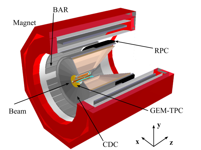
To test the performance of the large GEM-TPC it was installed inside the FOPI [27] experiment at GSI (Darmstadt, Germany), a large-acceptance spectrometer designed to study the properties of compressed nuclear matter produced in heavy-ion collisions at energies from to . The detector system has an almost complete azimuthal symmetry and nearly 4 coverage of the solid angle. It consists of a central drift chamber (CDC), a scintillator barrel, and resistive plate chambers (RPC) arranged cylindrically around the target. The setup is operated inside a superconducting solenoid magnet. The barrel part is augmented by a system of forward detectors including a planar drift chamber (Helitron) and a plastic scintillator wall (PLAWA). The GEM-TPC was mounted inside the inner bore of the CDC, supported only on the upstream side at the media flange by a light-weight ring-shaped structure made of carbon fiber. A schematic cross-section of all FOPI barrel sub-detectors, including the TPC, is shown in Fig. 40.
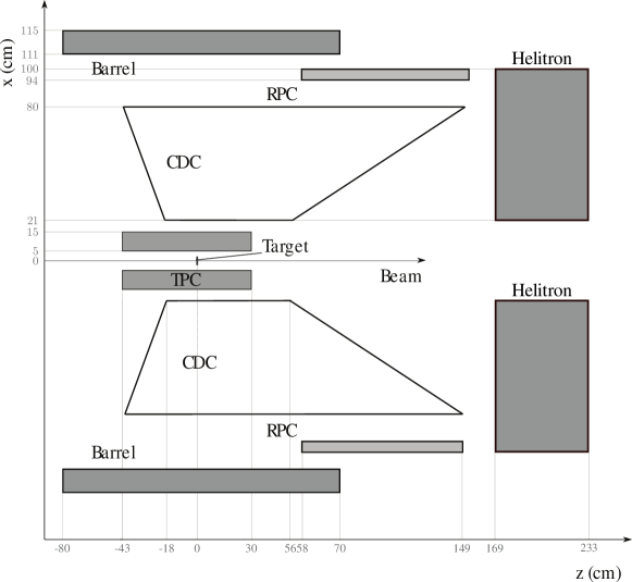
Figure 41 shows a three-dimensional model of the FOPI barrel system.
FOPI is able
to identify light charged particles like pions, kaons and protons and
intermediate mass fragments. Hadron resonances and neutral hadrons
can also be reconstructed from their decay products.
Before the installation of the GEM-TPC, the FOPI spectrometer
delivered a vertex resolution of about
in the plane and along the beam axis. The
momentum resolution for charged particles was
. The motivation to
install the GEM-TPC in FOPI was threefold: (i) the barrel detectors
provided a full-fledged magnetic spectrometer and thus and ideal
reference environment to test the GEM-TPC in different beams including heavy-ion
interactions, (ii) the GEM-TPC was expected to improve substantially the
vertex and
secondary vertex resolutions of the spectrometer, and (iii)
with its large
geometrical acceptance covering both barrel and forward detectors, the
GEM-TPC was supposed to
improve the inter-connection between these different sub-detector
elements.
The commissioning and operation of the GEM-TPC installed in FOPI was done in several phases. In the first phase, which started in October 2010, the TPC was commissioned with cosmic muons without and with the solenoid magnetic field. Data with cosmics were also taken in 2011 and 2012 for more detailed studies of the detector performance [30], which will be reported on in a forthcoming publication. In the second phase the stability of the GEM-TPC in collisions of different heavy-ion beams with nuclear targets was tested in November 2010 and April 2011. The third phase consisted of a three-week period of stable operation of the GEM-TPC during the FOPI S339 physics campaign in June 2011 with a pion beam impinging on solid targets. For this secondary beam only a rate of 25.000 /spill with a total spill length of and a duty cycle factor of was available. The major aim of this experiment was to measure charged and neutral kaons produced almost at rest in a nuclear medium. The data taken during this period resulted in the first measurement of the specific energy loss over a wide momentum range with a large GEM-TPC [38]. The physics results from this beam time [39] will be the subject of a forthcoming publication.
During the first two phases, two different gas mixtures, Ar/CO2 (90/10) and a Ne/CO2 (90/10), and several different field configurations were tested, both for the drift field and for the GEM stack. For the GEM stack, two categories of settings were used: the Standard Setting, optimized for stable operation in hadron beams and derived from the COMPASS experiment [13], and the so-called Ion Backflow Settings, which were found to minimize the ion backflow in a triple-GEM setup [40]. The values for the fields and GEM potential differences corresponding to these two categories for a gas gain of , respectively, are displayed in Table 5. Since the GEM-TPC is normally operated at a lower gain of , all potentials except the drift field are scaled down from the values given in the table by an overall scaling factor.
| Standard Setting | Ion Backflow Setting | |||
|---|---|---|---|---|
| Drift Field | ||||
| UGEM1 | ||||
| Etrans1 | ||||
| UGEM2 | ||||
| Etrans2 | ||||
| UGEM3 | ||||
| EInd | ||||
-
1.
Several drift fields have been applied: with the corresponding drift velocities: [41].
-
2.
Different voltage settings for the GEM-stack resulting in different gains have been tested ranging from .
-
3.
Two gas mixtures, namely Ar/CO2 and Ne/CO2 have been used, both in a mixture by weight.
The third phase (physics campaign) was conducted with the Ar-based gas mixture at a drift field of and a GEM gas gain of achieved at a scaling factor of of the standard GEM settings (second column in Table 5).
11.1 Tracks from Cosmic Muons
In the first phase, tracks from cosmic rays were measured using the scintillator barrel of FOPI as a trigger. Figure 42 shows the online event display for a typical cosmic muon track traversing the chamber and producing additional -electrons. This event was registered without a magnetic field and with the following settings for the TPC: a drift field of with an Ar/CO2 (90/10) mixture, which translates into a drift velocity of , and a GEM potential scaling factor of for standard settings.
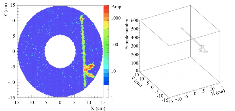
Various drift, gain, and gas settings were measured with cosmic muons in order to get a comprehensive picture of the detector performance, especially in terms of spatial resolution.
11.2 Tracks from Beam Interactions
Several beam species were utilized to collect data for the joint GEM-TPC/FOPI system during two test experiments at GSI in November 2010 and April 2011: 84Kr, 197Au and 22Ne beams at , , and kinetic energies, respectively, impinging on an Al target with of a nuclear interaction length placed in the inner bore of the GEM-TPC. The beam parameters were set to an average particle rate of 5106 particles/spill with a total spill length of about and a duty cycle factor of .
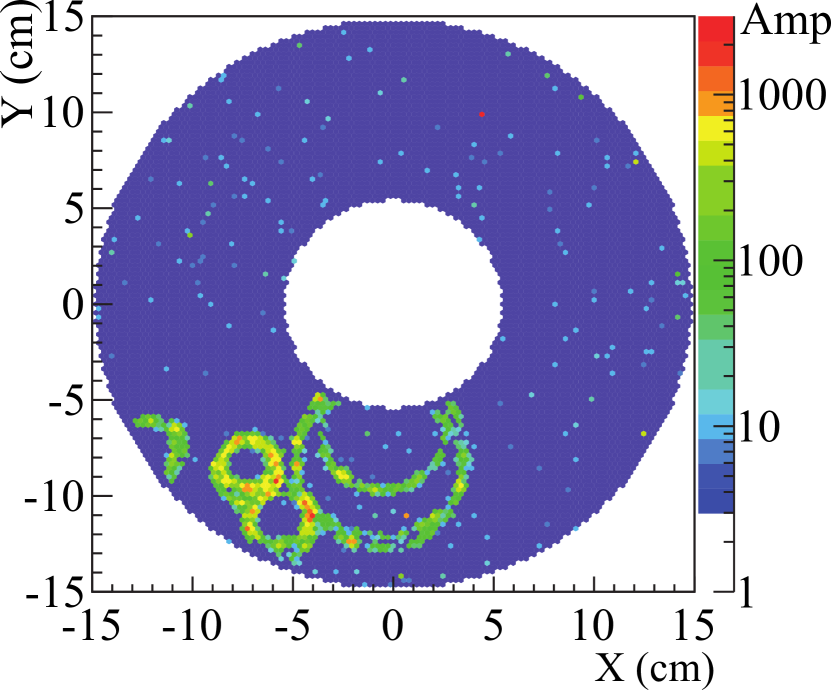
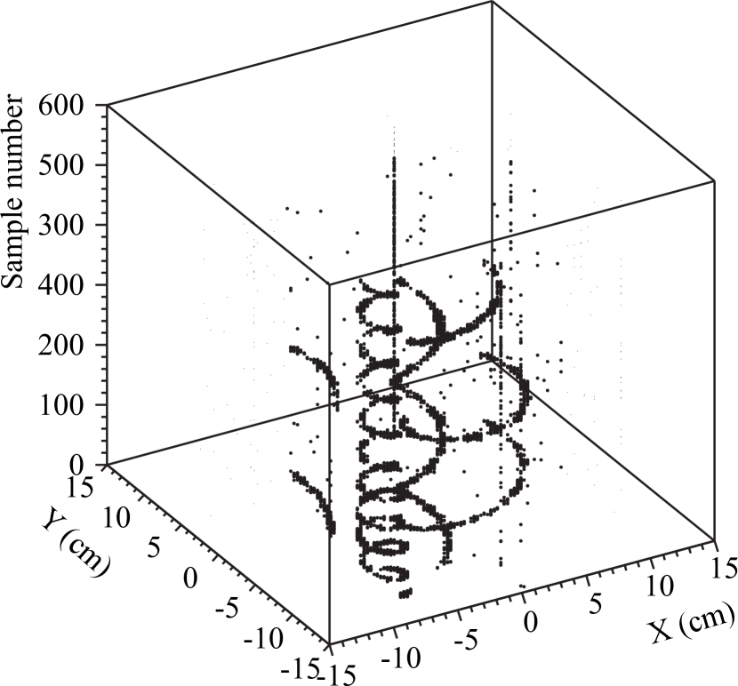
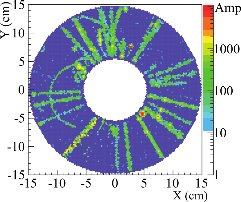
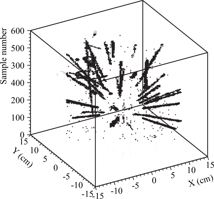
Figure 43 shows two typical events in the GEM-TPC for 22Ni+Al reactions. The chamber settings during this test were drift field in the Ar/CO2 (90/10) mixture and a GEM scaling factor of for standard settings. The top row shows an event where the beam particle presumably interacted upstream of the target, producing tracks almost parallel to the beam axis and several low-momentum particles curling in the magnetic field. In the bottom row an interaction in the Al target is displayed which produced a large number of charged particles.
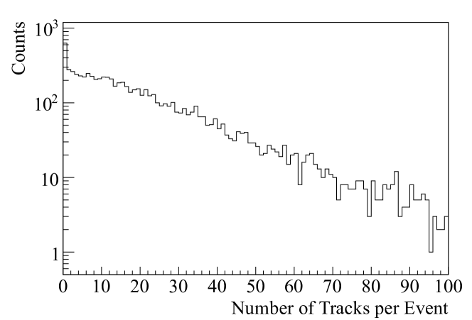
These online event displays provide direct evidence for the excellent 3-D tracking capability of a TPC, where the large density of hits along a particle track facilitates pattern recognition even in high-multiplicity events. Figure 44 shows the track multiplicity, i.e. the distribution of the number of reconstructed tracks per event, in the GEM-TPC for 22Ne+Al collisions at . As one can see, events with up to 100 tracks were successfully reconstructed.
For track fitting, the track segments in the TPC with an average length of are combined with the longer segments in the CDC. This allows the determination of particle momenta exceeding , for which the curvature in the GEM-TPC alone is too small.
12 Calibration procedures
A TPC requires a number of calibration procedures to be performed at regular intervals in order to achieve the design performance. For the GEM-TPC, the following calibration steps were implemented and applied:
-
1.
pedestal and noise determination,
-
2.
gain determination and equalization,
-
3.
drift velocity calibration.
They will be described in the following subsections.
While the first procedure is done on a sample-by-sample basis for each channel separately, the other two require a reconstruction of signals from the digitized data. The full set of algorithms to reconstruct particle tracks in the TPC will be described in a forthcoming publication ; here, we limit ourselves to the description of the algorithms to generate so-called reconstruction clusters, or simply clusters, which then also provide the input for the tracking algorithms.
12.1 Cluster Reconstruction
As a first step, consecutive samples of each pad with amplitudes above a given threshold are combined to so-called pad hits by using a simple pulse shape analysis (PSA) technique. Samples belonging to one pulse are identified by a search for local minima. The pad hit gets assigned a total signal charge (the sum of all associated sample amplitudes above threshold) and a signal time (time of the peak sample minus a constant offset of which takes into account the rise time of the signal). In the second step, accumulations of pad hits in 3-D space are further compressed into clusters in order to reduce the amount of data and further suppress noise hits. The clustering procedure starts from the pad hit with the highest amplitude in a given drift frame and adds pad hits both from neighboring pads on the pad plane and along the drift direction if they are sufficiently close in time. The hit association to a given cluster stops at local minima of the hit amplitude and a new cluster is started at the remaining pad hit with the highest amplitude until all pad hits are taken into account. Then a cut is applied on clusters consisting of only one pad hit, which effectively removes electronic noise hits. The total amplitude of a cluster is given by the sum of the amplitudes of the associated pad hits, its position is calculated as the center of gravity of the associated pad hits.
12.2 Pedestal and noise determination
In order to cope with the large amount of data from the TPC, noise
hits are suppressed already during data taking after digitization in
the ADC, as described in Sec. 7.4. The zero
suppression logic is implemented in a Xilinx Virtex-4 FPGA on the
ADC card and consists of baseline (pedestal) subtraction with
individual values for each channel, common mode and fixed pattern
noise correction for all channels connected to one side of the chip
packaging, and suppression of all channels with amplitudes smaller
than a threshold defined by a programmable multiple (typically between
and )
of the individual noise value of the given channel.
The pedestal and noise values for each channel are determined in
regular so-called pedestal runs. In these runs, which are performed at
nominal chamber conditions but without beam, a random trigger is used
to read out a small number of samples of each channel without zero
suppression. The number of samples per channel is limited to typically
6–10 by the bandwidth of the readout chain. From this data sample,
the average (pedestal) and the rms width (noise in ADC channels or
equivalent noise charge, ENC, if converted to charge) of the recorded
baseline values are determined offline for each channel and saved in a
file. The values in the file are then uploaded to the ADC card using
the I2C protocol and applied to the raw data when zero suppression is
activated.
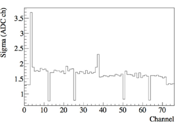
The noise values of all channels of one front-end chip can be seen in
Fig. 45 (left). The distribution of the noise values for
all 10254 channels connected to the pad plane is shown in
Fig. 45 (right). There are two groups of channels with a
slightly offset noise distribution, related to the signal paths on the
front-end card. The first 36 channels of each chip have longer input
lines than the second 36 channels. This reflects in a slightly
different noise level of these groups of channels, as can be seen from
Fig. 45. The outlier channels with higher noise are
typically the ones on the edges connected to the
far side of the chip pins.
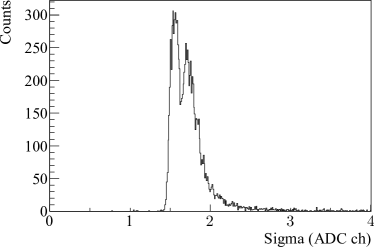
The average noise (including the tails) of all channels is 1.83 ADC channels, corresponding to an equivalent noise charge of . The most probable values of the ENC for the two groups of channels are and , for input capacitances of and , respectively. Figure 46(a) shows the pedestals values for all pads of the pad-plane in units of ADC channels, while Fig. 46(b) displays their noise values.
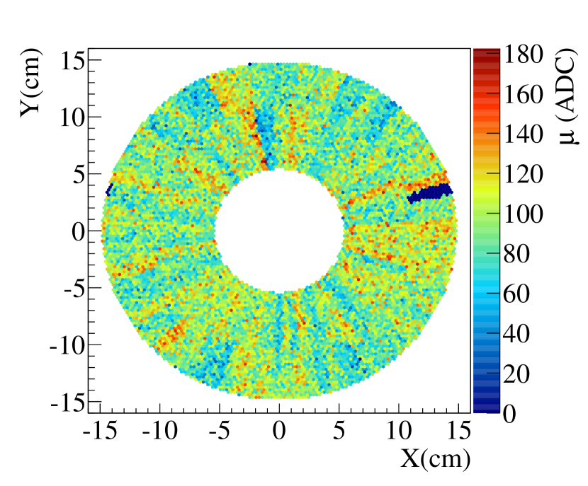
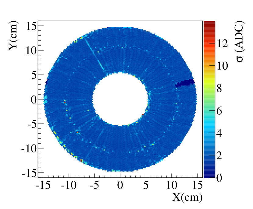
The ring structure with a higher noise level, which can be seen in Fig. 46(b) is caused by channels on the edges of the block with longer track lengths from the connector to the chip on the front-end PCB.
12.3 Calibration of the gas gain
The gas gain is one of the key parameters which decisively influences
the performance of the TPC in terms of spatial and energy
resolution. For GEM detectors, the effective gain of the GEM stack is
the important quantity, because it takes into account charge losses in
the GEM structures. Using an X-ray source with known rate, it may be
determined e.g. from the current measured on the readout pads. In
addition to the absolute value of the effective gain, which determines
the signal-to-noise ratio, local relative variations of it strongly
impact the energy resolution of the detector and thus the
resolution. In multi-GEM detectors, such
variations may arise from non-uniformities of the hole diameters or
the foil spacings across the active area, and have been observed to be
as large as [42]. Contributions to
local variations of the gain can also originate from slightly varying
electronic conversion gains for individual channels of the front-end
chips. In order not to compromise the
resolution of the detector, a gain homogeneity of
across the GEM surface has to be achieved by a proper
calibration. An elegant method to monitor and equalize the total gain
(effective gas gain and electronic conversion gain) for each pad
during data taking is by introducing metastable radioactive
into the drift volume. This technique does not require any physical
invasion of the detector and allows full coverage of its active
volume, and has already been applied in various large TPCs (e.g. ALEPH
[43], DELPHI [44], HARP [45],
ALICE
[9], STAR [46]).
In order to introduce 83mKr into the GEM-TPC, a dedicated
83Rb source with an activity of was
produced at the HISKP222Helmholtz-Institut für Strahlen- und
Kernphysik, Nussallee 14-16, D-53115 Bonn cyclotron
[47].
83Rb decays with a half-life of
via electron capture into 83Kr, mostly populating
an isomeric, metastable state at with a half-life of
. This state decays into the ground state via a
short-lived excited state at . Both
transitions occur predominantly via internal conversion, producing
short-ranged electrons. The resulting shell excitation is removed by
X-rays or Auger electrons. The decay spectrum observed in the TPC
thus shows several peaks between and
.
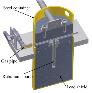
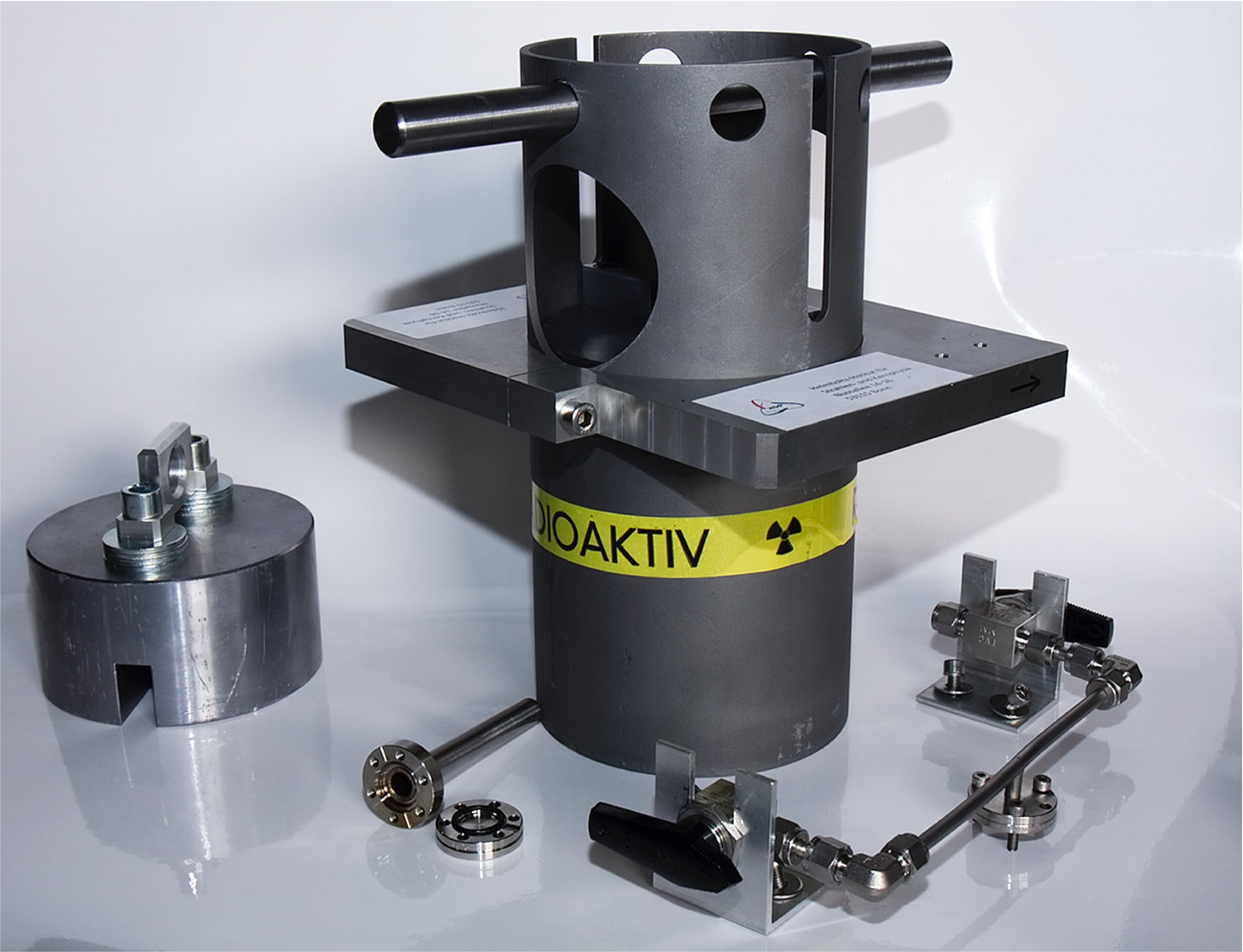
The container for the 83Rb source can be seen in Fig. 47. It is connected to the gas input line of the GEM-TPC such that, when the corresponding valves are opened, the gas flows past the inner steel tube holding the radioactive material, carrying the evaporated 83mKr into the chamber volume. The container shielding consists of lead that absorbs higher energetic decay photons.

During normal operation of the TPC
the Rb container is bypassed.
Dedicated Kr calibration runs have been performed regularly during
beam times using a random trigger. The electrons emitted in the decay
process are stopped quickly in the gas and lead to large but spatially
confined clusters which are reconstructed using the reconstruction
techniques described at the beginning of this
section. Figure 49(a) shows an example of typical clusters
created by Kr decays.
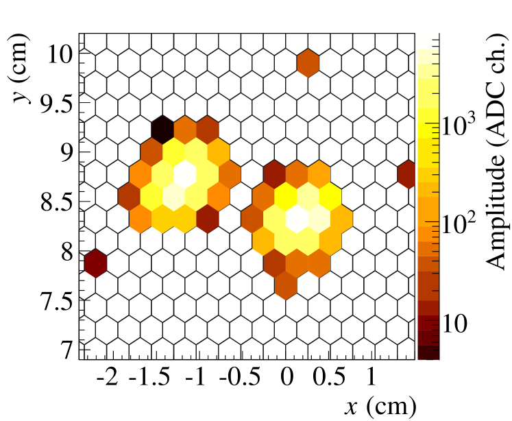
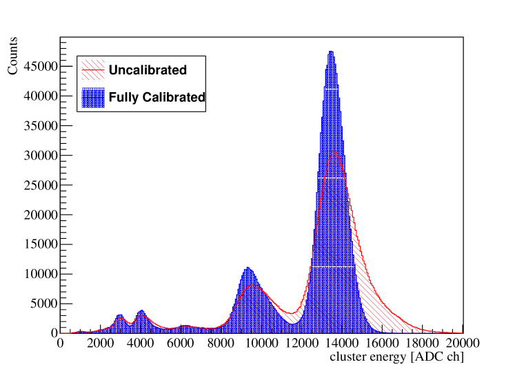
The total cluster amplitude spectrum (in units of ADC channels) measured in Ar/CO2 (90/10) is shown in Fig. 49(b). It depends on the deposited energy , the mean energy required to create an electron-ion pair in the gas , the effective gain and the conversion gain of the readout system, measured in (see section 7.5):
| (1) |
With and known, the absolute effective gain can be calibrated by reconstructing the full energy () deposit of Kr decays. The resulting gain curve is displayed in Fig. 50 as a function of the scale factor applied to all GEM potentials (cf. Table 5 for the definition of the nominal setting corresponding to ).
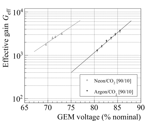
For Ar/CO2 (90/10), a gain of approx. 2000 is achieved at a scale
factor of .
For a sufficiently large data sample this procedure also allows to
extract pad-wise gain variations.
To this end, the total charge of a reconstructed Kr cluster is
assigned to the pad which contributed the pad hit with the largest
amplitude, and an amplitude histogram is generated for every single
pad. Only pads/channels with more than 500 entries are used for
calibration. Pads with a distance to the outer or inner field-cage
smaller than are not taken into account as edge effects
introduced by the field-cage walls deteriorate the measurement of the
total charge.
Finally, the gain equalization is performed by moving the median
position of the main decay peak () for
all individual channels to the overall median position. From the
relative shift a relative gain map is generated which is normalized to
1. The median was found to be less sensitive to outliers or values
from failed fits than the mean.
The relative calibration is done iteratively re-running the whole
reconstruction and recursively correcting the gain factors.
Figure 51 shows the relative gain correction factors as a
function of the pad positions obtained after 3 iterations. Pads with
insufficient or no data (e.g. pads close to the field cage walls or
broken electronic channels) are set to have correction factors of
1. Clearly visible are the sector boundaries of the last two GEM
foils, slightly rotated with respect to each other, with a lower
effective gain (i.e. correction factor ). In addition, a darker,
cross-shaped pattern is visible, most likely caused by stress applied
during the glueing or mounting of the GEM stack. In these regions of
larger foil tension, an increase in effective gain is observed
(correction factors ).
Figure 51(b) shows a histogram of all gain calibration
factors. The underlying distribution centered at 1 has an RMS of
. The sharp peak at 1 comes from channels whose
calibration factor was set to 1.
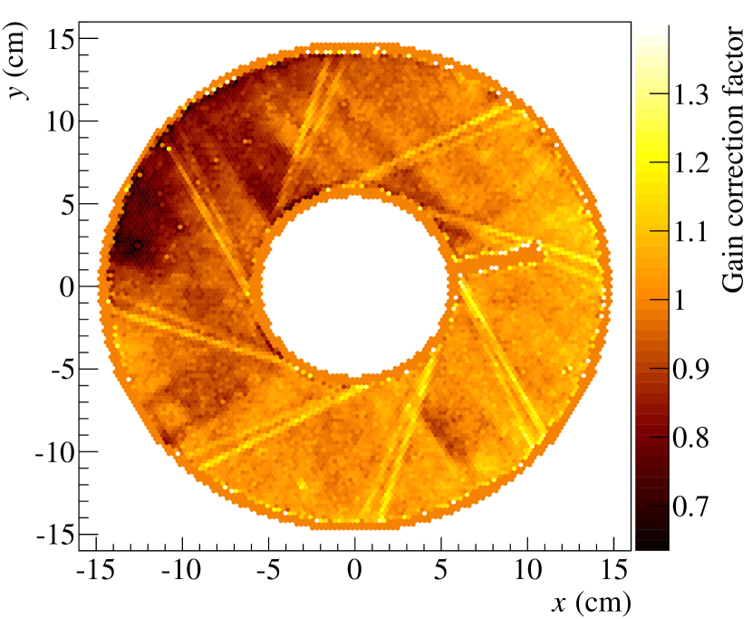
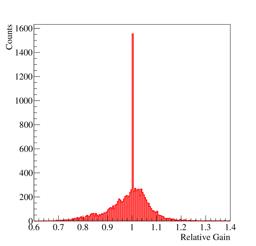
The Kr cluster amplitude spectrum measured with the GEM-TPC in
Ar/CO2 (90/10) gas at a voltage scaling factor of is shown
in Fig. 49(b) before (red) and after (blue) applying
the pad-wise relative gain calibration. A clear separation of the
main peaks can be observed while the double-peak-structure at
can not be clearly separated. An
energy resolution of before and
after calibration in the main peak is
achieved, i.e. the pad-wise calibration enhances the energy
resolution of the detector at by more than . This
translates into an improvement of on the specific-energy
resolution of the GEM-TPC [38, 39].
An important quantity which influences both the position and the
energy resolution of the detector is the signal-to-noise ratio
(SNR). It is defined as the maximum pad signal amplitude in a cluster
divided by the corresponding pad noise value. Typically, the SNR is
required be larger than 20 – 25 for TPCs [48]. The
signal-to-noise ratio for the GEM-TPC for different values of the gas
gain in Ar/CO2 (90/10) is shown in Fig. 52.
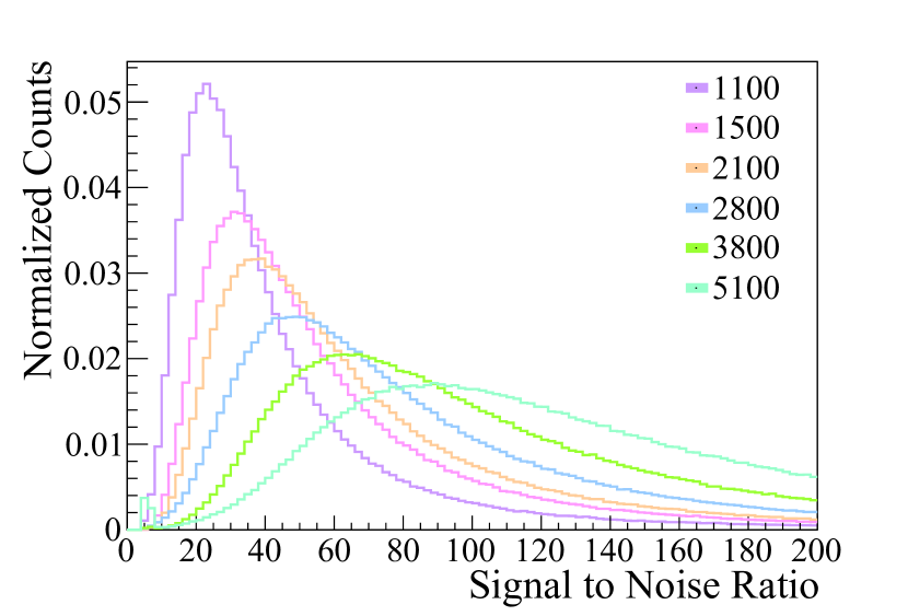
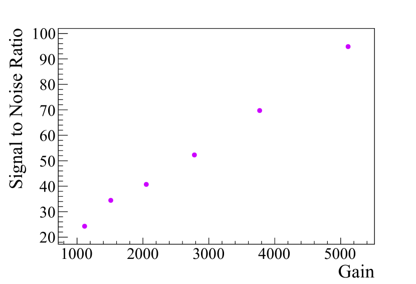
12.4 Determination of the drift velocity
The resolution of a TPC relies critically on the knowledge of the
drift velocity of electrons. The drift velocity depends on many
parameters such as the exact gas mixture, potential impurities like
water and oxygen, the temperature and pressure of the gas, and the
exact values of the electric and magnetic fields. Since not all of
these parameters might be known with the required accuracy, it is
important to be able to
determine the drift velocity in situ from the data.
If the maximum drift time of electrons in the TPC is smaller than the
readout time window given by the product of the maximal number of
samples (511) and the time length per sample ( for a
sampling frequency of ), the full drift window of the TPC
is read out.
The average drift velocity can then be determined using the drop of
the cluster occupancy at the geometric boundaries imposed by the
cathode and the GEM foil closest to the drift volume. The measured
cluster occupancy distribution as a function of the time obtained from
cosmic muon data at a drift field of is shown
in Fig. 53.
The clusters used for this procedure are constructed as described in
12.1. Table 6 shows the cuts
applied to select good clusters and to reduce background
contributions.
| selection criteria | Value |
|---|---|
| cluster size | 2 pad hit |
| cluster amplitude | 50 ADC channels |
| radial position (min.) | |
| radial position (max.) |
Error functions are fitted to the occupancy distribution in order to determine the position of the cathode and the first GEM foil. The inflection points of these functions are used to determine the edges of the drift volume.
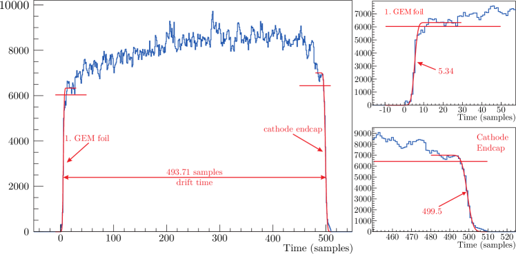
With the difference between the two edges in units of ADC samples, , the sampling rate of the front-end chip and the known distance between the chamber edges, the drift velocity averaged over the full volume can be calculated by
| (2) |
The same method can also be used for measurements with particle beams,
provided the drift velocity is large enough so that the full drift
length is visible. In Fig. 54 one can see a
cluster time spectrum obtained with a beam at
a drift field of in Ar/CO2 (90/10)
gas. Two targets were installed in the central bore of the TPC, a Pb
and a Cu disk further downstream, which are visible as
pronounced drops in the occupancy in Fig. 54. In
case the physical boundaries of the drift volume are not visible,
e.g. because of a smaller drift field, the known target positions may
be used to perform the drift velocity calibration instead
[37].
Figure 55 shows the time evolution of drift
velocities determined by fitting the end-cap positions for different
data taking periods (left: pion beam, right: cosmics), compared
to drift velocities calculated with Magboltz
[49]. These take into account the gas temperatures and
pressures measured at the inlet to the TPC located in the media
flange. The uncertainties shown for the Magboltz calculation take
into account the variations of the pressure and temperature
measurements around their average values. The uncertainties for the
measured values are the statistical uncertainties of the error
function fits.
One can see that the relative differences between measurement and
Magboltz calculations are below for the pion beam
measurement and in between and for
the cosmic muon measurement.
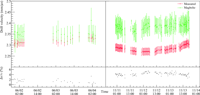
The systematic shift between measured and calculated drift velocity is attributed to a possible bias in the temperature and pressure measurements, which may not reflect the actual gas conditions and to a systematic uncertainty of the actual drift length. For the future, it is planned to extract the drift velocity from the alignment procedure using particle tracks which are measured both in the GEM-TPC and the CDC of the FOPI experiment. In addition, a more precise measurement of the actual gas pressure and temperature is envisaged.
13 Conclusions
A large TPC with GEM amplification and without gating grid was built and successfully tested to demonstrate its applicability in future high-rate experiments such as ALICE at CERN. The detector features a number of innovative elements such as an extremely light-weight and gas-tight vessel, which serves as field cage and gas container at the same time, a stack of large disk-shaped sectorized GEM foils integrated in a media flange which forms the detector end cap, or a readout plane with hexagonal pads in order to minimize the pad angular effect. The signals induced on the pad-plane are read out using AFTER/T2K ASICs mounted on fully custom-made front-end cards and ADCs.
First commissioning results of the system have been shown, which prove the feasibility of this novel detector type. The chamber itself as well as all custum-made supporting infrastructure such as the cooling circuit, the gas supply, and the slow-control system have shown excellent performance during data taking with cosmic rays and various particle beams as part of the FOPI spectrometer. Calibration procedures have been established and put into operation, such as pedestal and noise determination, gain calibration and equalization based on the injection of metastable 83Kr into the detector gas, and drift velocity determination.
These results raise the expectation that (i) the GEM-TPC will significantly improve the performance of the FOPI experiment by enhancing the vertex resolution, the secondary vertex reconstruction and the global event reconstruction, and that (ii) an ungated TPC with GEM amplification will allow us to overcome the large deadtime associated with classical TPCs, and thus open many new areas of application of this powerful detector type.
Acknowledgements
We express our gratitude to the engineers and technicians from GSI Darmstadt, TU München, Universität Bonn, and SMI Vienna, who have contributed to the construction and commissioning of the GEM-TPC.
We acknowledge support from Bundesministerium für Bildung und Forschung, (Grant agreement no. 06MT245I, 06MT9165I, 05P12WOCAA, 05P12WOGHH), DFG cluster of excellence “Origin and Structure of the Universe”, DFG SFB/TR16 “Elektromagnetische Anregung subnuklearer Systeme”, GSI Forschungs- und Entwicklungsauftrag (Grant agreement no. TMPAUL, TMPAUL1012, TMFABI1012, TMLFRG1316F), Helmholtz Association (Young Investigator Group VH-NG-330), European Union FP7 (HadronPhysics2, Grant agreement no. 227431; HadronPhysics3, Grant agreement no. 283286).
References
- [1] D. R. Nygren, J. N. Marx, The Time Projection Chamber, Phys. Today 31N10 (1978) 46–53.
- [2] R. J. Madaras, et al., Spatial resolution of the PEP-4 Time Projection Chamber, IEEE Trans. Nucl. Sci. 30 (1983) 76–81.
- [3] W. B. Atwood, et al., Performance of the ALEPH time projection chamber, Nucl. Instr. Meth. A 306 (1991) 446–458. doi:10.1016/0168-9002(91)90038-R.
- [4] C. Brand, et al., The DELPHI Time Projection Chamber, Nucl. Instr. Meth. A 283 (1989) 567–572. doi:10.1109/23.34417.
- [5] S. Wenig, Performance of the large-scale TPC system in the CERN heavy ion experiment NA49, Nucl. Instr. Meth. A 409 (1998) 100–104. doi:10.1016/S0168-9002(97)01245-X.
- [6] S. Afanasev, et al., The NA49 large acceptance hadron detector, Nucl. Instr. Meth. A 430 (1999) 210–244. doi:10.1016/S0168-9002(99)00239-9.
- [7] K. H. Ackermann, et al., The STAR time projection chamber, Nucl. Phys. A 661 (1999) 681–685. doi:10.1016/S0375-9474(99)85117-3.
- [8] K. H. Ackermann, et al., The forward time projection chamber (FTPC) in STAR, Nucl. Instr. Meth. A 499 (2003) 713–719. arXiv:nucl-ex/0211014, doi:10.1016/S0168-9002(02)01968-X.
- [9] J. Alme, et al., The ALICE TPC, a large 3-dimensional tracking device with fast readout for ultra-high multiplicity events, Nucl. Instr. Meth. A 622 (2010) 316–367. arXiv:1001.1950, doi:10.1016/j.nima.2010.04.042.
- [10] G. Charpak, R. Bouclier, T. Bressani, J. Favier, C. Zupancic, The use of multiwire proportional counters to select and localize charged particles, Nucl. Instr. Meth. 62 (1968) 262–268.
- [11] F. Sauli, GEM: A new concept for electron amplification in gas detectors, Nucl. Instr. Meth. A 386 (1997) 531–534.
- [12] F. Sauli, S. Kappler, L. Ropelewski, Electron collection and ion feedback in GEM-based detectors, in: Nuclear Science Symposium Conference Record, 2002. NSS ’02. IEEE, IEEE, Piscataway, NJ, 2002.
- [13] C. Altunbas, M. Capeáns, K. Dehmelt, J. Ehlers, J. Friedrich, I. Konorov, A. Gandi, S. Kappler, B. Ketzer, R. D. Oliveira, S. Paul, A. Placci, L. Ropelewski, F. Sauli, F. Simon, M. van Stenis, Construction, test and commissioning of the triple-GEM tracking detectors for COMPASS, Nucl. Instr. Meth. A 490 (2002) 177–203.
-
[14]
B. Ketzer, Q. Weitzel, S. Paul, F. Sauli, L. Ropelewski,
Performance
of triple GEM tracking detectors in the COMPASS experiment, Nucl. Instr.
Meth. A 535 (1) (2004) 314–318.
doi:10.1016/j.nima.2011.06.028.
URL http://www.sciencedirect.com/science/article/pii/S0168900211011442 - [15] P. Abbon, et al., The COMPASS experiment at CERN, Nucl. Instr. Meth. A 577 (2007) 455–518. arXiv:hep-ex/0703049.
- [16] B. Ketzer, A. Austregesilo, F. Haas, I. Konorov, M. Krämer, A. Mann, T. Nagel, S. Paul, A triple-gem detector with pixel readout for high-rate beam tracking in compass, in: Nuclear Science Symposium Conference Record, 2007. NSS ’07. IEEE, Vol. 1, IEEE, Piscataway, NJ, 2007, pp. 242–244. doi:10.1109/NSSMIC.2007.4436323.
- [17] G. Bencivenni, et al., A triple GEM detector with pad readout for high rate charged particle triggering, Nucl. Instr. Meth. A 488 (2002) 493–502. doi:10.1016/S0168-9002(02)00515-6.
- [18] Z. Fraenkel, et al., A hadron blind detector for the PHENIX experiment at RHIC, Nucl. Instr. Meth. A 546 (2005) 466–480. arXiv:physics/0502008, doi:10.1016/j.nima.2005.02.039.
- [19] M. G. Bagliesi, et al., The TOTEM T2 telescope based on triple-GEM chambers, Nucl. Instr. Meth. A 617 (2010) 134–137. doi:10.1016/j.nima.2009.07.006.
- [20] G. Bencivenni, D. Domenici, An ultra-light cylindrical GEM detector as inner tracker at KLOE-2, Nucl. Instr. Meth. A 581 (2007) 221–224. doi:10.1016/j.nima.2007.07.082.
- [21] D. Abbaneo, et al., Characterization of GEM Detectors for Application in the CMS Muon Detection SystemarXiv:1012.3675.
- [22] M. Ball, K. Eckstein, T. Gunji, Ion backflow studies for the ALICE TPC upgrade with GEMs, JINST 9 (2014) C04025. doi:10.1088/1748-0221/9/04/C04025.
-
[23]
ALICE collaboration, Addendum to
the Technical Design Report for the Upgrade of the ALICE Time Projection
Chamber, Tech. Rep. CERN-LHCC-2015-002. ALICE-TDR-016-ADD-1, CERN, Geneva
(Feb 2015).
URL https://cds.cern.ch/record/1984329 - [24] B. Ketzer, A Time Projection Chamber for High-Rate Experiments: Towards an Upgrade of the ALICE TPC, Nucl. Instr. Meth. A 732 (2013) 237–240. arXiv:1303.6694, doi:10.1016/j.nima.2013.08.027.
-
[25]
ALICE collaboration, Upgrade of
the ALICE Time Projection Chamber, Tech. Rep. CERN-LHCC-2013-020.
ALICE-TDR-016, CERN, Geneva (Oct 2013).
URL https://cds.cern.ch/record/1622286 - [26] M. Lang, Upgrade for the CBELSA/TAPS experiment at ELSA for eta and eta-prime decays, Int. J. Mod. Phys. E19 (2010) 938–945. doi:10.1142/S0218301310015382.
- [27] K. Hildenbrand, One year of operating FOPI: Results and status of the detector facility at SIS/ESR, GSI Nachr. 91-02 (1992) 6–16.
- [28] R. Brun, F. Rademakers, ROOT - An object oriented data analysis framework, Nuclear Instruments and Methods in Physics Research Section A: Accelerators, Spectrometers, Detectors and Ass ociated Equipment 389 (1–2) (1997) 81 – 86, new Computing Techniques in Physics Research V. doi:http://dx.doi.org/10.1016/S0168-9002(97)00048-X.
- [29] S. Bachmann, A. Bressan, M. Capeáns, M. Deutel, S. Kappler, B. Ketzer, A. Polouektov, L. Ropelewski, F. Sauli, E. Schulte, L. Shekhtman, A. Sokolov, Discharge studies and prevention in the gas electron multiplier (GEM), Nucl. Instr. Meth. A 479 (2002) 294–308, CERN-EP-2000-151.
- [30] M. Berger, Development, Commissioning and Spatial Resolution Studies of a new GEM based TPC, Ph.D. thesis, Technische Universtiät München (2015).
-
[31]
S. Barboza, M. Bregant, et al.,
SAMPA chip: a new
ASIC for the ALICE TPC and MCH upgrades, Journal of Instrumentation
11 (02) (2016) C02088.
URL http://stacks.iop.org/1748-0221/11/i=02/a=C02088 - [32] C. Hearty, et al., T2K ND 280 TPC technical design report version 1.0T2K Internal Note.
- [33] P. Baron, et al., AFTER, an ASIC for the readout of the large T2K time projection chambers, IEEE Trans. Nucl. Sci. 55 (2008) 1744–1752. doi:10.1109/TNS.2008.924067.
- [34] G. Baum, et al., COMPASS: A proposal for a COmmon Muon and Proton Apparatus for Structure and Spectroscopy, CERN/SPSLC 96-14, SPSC/P 297 (March 1996).
- [35] Huber Kältemaschinenbau GmbH, UCH080T-H, www.huber-online.com.
- [36] Phillip Müllner, A GEM based Time Projection Chamber prototype for the PANDA experiment - Gas system development and forward tracking studies, Ph.D. thesis, Universtiät Wien (2012).
-
[37]
D. Kaiser, Steuerung und
Überwachung einer Zeitprojektionskammer mit GEM-Auslese, Ph.D.
thesis, Rheinische Friedrich-Wilhelms-Universität Bonn (2014).
URL http://hss.ulb.uni-bonn.de/2014/3530/3530.htm - [38] F. Böhmer, M. Ball, S. Dørheim, K. Eckstein, A. Hönle, C. Höppner, B. Ketzer, et al., First measurement of with a GEM-based TPC, Nucl. Instr. Meth. A 737 (2014) 214–221. doi:10.1016/j.nima.2013.10.094.
- [39] F. Böhmer, Development of a GEM-based TPC for the measurement of in-medium signatures in kaon momenta in a combined setup at fopi, Ph.D. thesis, Techn. Univ. München (2015).
- [40] M. Ball, F. Böhmer, S. Dørheim, C. Höppner, B. Ketzer, et al., Technical Design Study for the PANDA Time Projection ChamberarXiv:1207.0013.
- [41] F. Sauli, Principles of operation of multiwire proportional and drift chambers, CERN, CERN, Geneva, 1977, p. 92 p, CERN, Geneva, 1975 - 1976.
- [42] L. Hallermann, Analysis of GEM properties and development of a GEM support structure for the ILD Time Projection Chamber, Ph.D. thesis, DESY (2010).
- [43] D. Decamp, B. Deschizeaux, et al., ALEPH: A detector for electron-positron annihilations at LEP, NIMA 294 (1-2) (1990) 121 – 178. doi:DOI:10.1016/0168-9002(90)91831-U.
- [44] A. De Min, et al., Performance of the HPC calorimeter in DELPHI, IEEE Trans. Nucl. Sci. 42 (1995) 491–498. doi:10.1109/23.467923.
- [45] F. Dydak, A. De Min, Analysis of harp tpc krypton data, HARP memo 04-103, submitted 28 April 2004 corrected 7 May 2004 updated 10 June 2004.
- [46] T. Eggert, Calibration of the STAR Forward Time Projection Chamber with Krypton-83m, Star Note 424.
- [47] M. Rasulbaev, K. Maier, R. Vianden, T. Thümmler, B. Ostrick, C. Weinheimer, Production of 83rb for the katrin experiment, Applied Radiation and Isotopes 66 (12) (2008) 1838 – 1843. doi:DOI:10.1016/j.apradiso.2008.04.020.
- [48] G. Dellacasa, et al., ALICE technical design report of the time projection chamber, Tech. rep., CERN (2000).
- [49] S. Biagi, Monte carlo simulation of electron drift and diffusion in counting gases under the influence of electric and magnetic fields, Nucl. Instr. Meth. A 421 (1 - 2) (1999) 234 – 240. doi:http://dx.doi.org/10.1016/S0168-9002(98)01233-9.